TH7120 300 to 930MHz FSK/FM/ASK Transceiver 3901007120 Page 1 of 28 Data Sheet Rev. 005 Jan. 2002 PR E L IM I NA R Y Features ! Single chip solution with only a few external components ! Stand-alone fixed-frequency transceiver operation modes ! Programmable multi-channel transceiver operation modes ! Low current consumption in active mode and very low standby current ! PLL-stabilized RF VCO (LO) with internal varactor diode ! Lock detection in programmable channel applications ! 3wire bus serial control interface ! FSK/ASK modulation selection ! FSK for digital data and FM for analog signal reception ! RSSI allows signal strength indication and ASK detection ! Switchable LNA gain for improved dynamic range ! Automatic PA turn-on after PLL lock ! FM possible with external varactor ! ASK modulation achieved by on/off keying ! AFC option for extended input frequency acceptance range ! Surface mount package LQFP32 Ordering Information Part No. (Engineering Samples) Temperature Code Package Code TH7120 (TH7120-03) E (-40 °C to 85 °C) NE (LQFP32) Application Examples ! General bi-directional half duplex digital data transmission or analog signal transmission ! Low-power telemetry ! Alarm and security systems ! Keyless car and central locking ! Domotics ! Model control Technical Data Overview ! Frequency range: 300 MHz to 930 MHz for programmable channel applications ! 315 MHz, 433 MHz, 868 MHz or 915 MHz fixed-frequency single-channel variants ! Power supply range: 2.5 V to 5.5 V ! Temperature range: -40 °C to +85 °C ! Standby current: 50 nA ! Operating current: 6.0 mA in receive mode at low gain ! Operating current 9.0 mA in transmit mode at 0 dBm output power ! Adjustable output power range from –15 dBm to +6 dBm ! Sensitivity: -103 dBm at FSK with 150 kHz IF filter BW ! Sensitivity: -105 dBm at ASK with 150 kHz IF filter BW ! Maximum data rate for FSK and ASK: 60 kbit/s NRZ ! Maximum input level: –10 dBm at FSK and -20 dBm at ASK ! Input frequency acceptance: ± 50 kHz (with AFC option) ! Frequency deviation range: ±5 kHz to ±100 kHz ! Maximum analog modulation frequency: 20 kHz ! 3 MHz to 12 MHz crystal reference

Welcome message from author
This document is posted to help you gain knowledge. Please leave a comment to let me know what you think about it! Share it to your friends and learn new things together.
Transcript
TH7120300 to 930MHz
FSK/FM/ASK Transceiver
3901007120 Page 1 of 28 Data SheetRev. 005 Jan. 2002
PRELIMINARY
Features! Single chip solution with only a few external components! Stand-alone fixed-frequency transceiver operation modes! Programmable multi-channel transceiver operation modes! Low current consumption in active mode and very low standby current! PLL-stabilized RF VCO (LO) with internal varactor diode! Lock detection in programmable channel applications! 3wire bus serial control interface! FSK/ASK modulation selection! FSK for digital data and FM for analog signal reception! RSSI allows signal strength indication and ASK detection! Switchable LNA gain for improved dynamic range! Automatic PA turn-on after PLL lock! FM possible with external varactor! ASK modulation achieved by on/off keying! AFC option for extended input frequency acceptance range! Surface mount package LQFP32
Ordering InformationPart No. (Engineering Samples) Temperature Code Package Code
TH7120 (TH7120-03) E (-40 °C to 85 °C) NE (LQFP32)
Application Examples! General bi-directional half duplex digital data transmission or analog signal transmission! Low-power telemetry! Alarm and security systems! Keyless car and central locking! Domotics! Model control
Technical Data Overview! Frequency range: 300 MHz to 930 MHz for programmable channel applications! 315 MHz, 433 MHz, 868 MHz or 915 MHz fixed-frequency single-channel variants! Power supply range: 2.5 V to 5.5 V! Temperature range: -40 °C to +85 °C! Standby current: 50 nA! Operating current: 6.0 mA in receive mode at low gain! Operating current 9.0 mA in transmit mode at 0 dBm output power! Adjustable output power range from –15 dBm to +6 dBm! Sensitivity: -103 dBm at FSK with 150 kHz IF filter BW! Sensitivity: -105 dBm at ASK with 150 kHz IF filter BW! Maximum data rate for FSK and ASK: 60 kbit/s NRZ! Maximum input level: –10 dBm at FSK and -20 dBm at ASK! Input frequency acceptance: ± 50 kHz (with AFC option)! Frequency deviation range: ±5 kHz to ±100 kHz! Maximum analog modulation frequency: 20 kHz! 3 MHz to 12 MHz crystal reference
TH7120300 to 930MHz
FSK/FM/ASK Transceiver
3901007120 Page 2 of 28 Data SheetRev. 005 Jan. 2002
PRELIMINARY
General Description
The TH7120 is a single chip FSK/FM/ASK transceiver IC. It is designed to operate in low-power multi-channelprogrammable or single-channel stand-alone, half-duplex data transmission systems. It can be used for ISM,SRD or any other application operating in the frequency ranging of 300 MHz to 930 MHz.
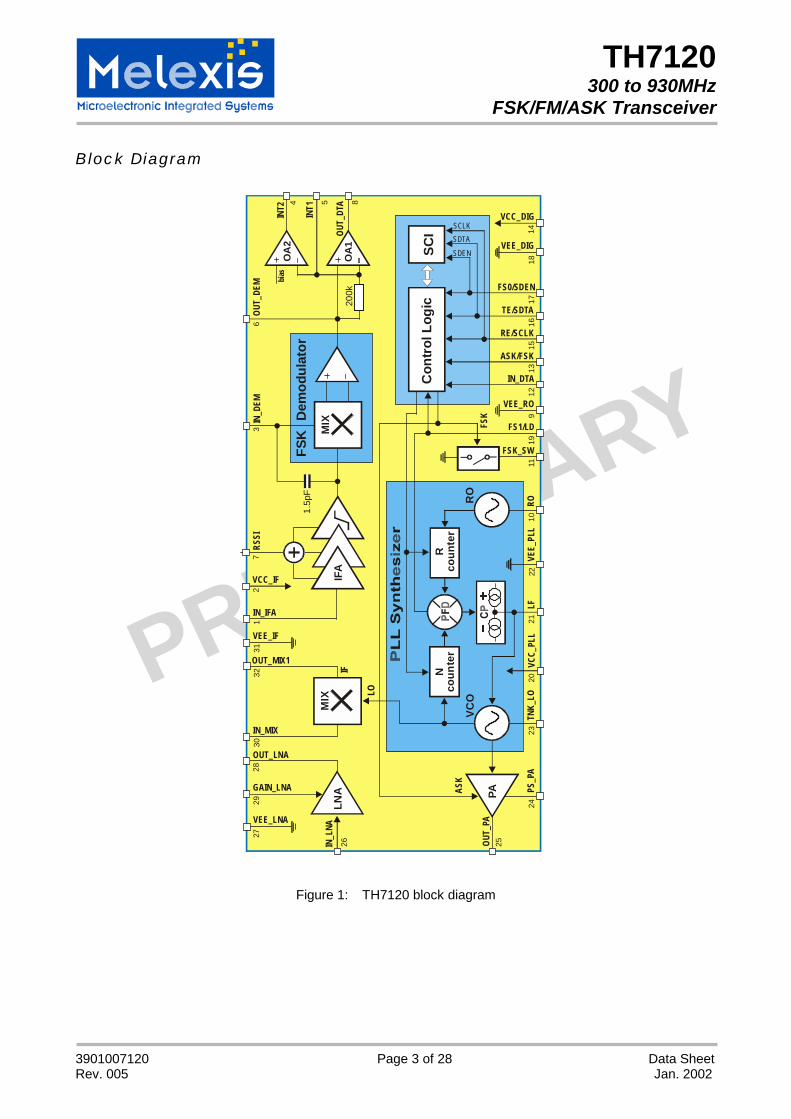
The TH7120 transceiver IC consists of the following building blocks:
" Low-noise amplifier (LNA) for high-sensitivity RF signal reception with switchable gain" Mixer (MIX) for RF-to-IF down-conversion" IF amplifier (IFA) to amplify and limit the IF signal and for RSSI generation" Phase-coincidence demodulator with external ceramic discriminator (FSK Demodulator)" Operational amplifier, connected to demodulator output (OA1)" Operational amplifier, integrator circuit at FSK-AFC mode (OA2)" Control logic with 3wire bus serial control interface (SCI)" Reference oscillator (RO) with external crystal" Reference divider (R counter)" Programmable divider (N/A counter)" Phase-frequency detector (PFD)" Charge pump (CP)" Voltage control oscillator (VCO) with internal varactor" Power amplifier (PA) with adjustable output power
The transceiver can be used either as a 3wire-bus-controlled programmable or as a stand-alone fixed-frequency device. After power up, the transceiver is set to fixed-frequency mode. In this mode, pinsFS0/SDEN and FS1/LD must be connected to VEE or VCC in order to set the desired frequency of operation.The logic levels at pins FS0/SDEN and FS1/LD must not be changed after power up in order to remain infixed-frequency mode.
Channel frequency 433.92 MHz 868.3 MHz 315.0 MHz 915.0 MHzFS0/SDEN 1 0 1 0FS1/LD 0 0 1 1
After the first logic level change at pin FS0/SDEN, the transceiver enters into programmable mode while pinFS1/LD is now a PLL lock detector output. In this mode, the user can set any PLL frequency or mode of op-eration by the SCI.
In the fixed-frequency mode, the user can set the transceiver to Standby, Receive, Transmit or Idle (only PLLsynthesizer active) mode via control pins RE/SCLK and TE/SDTA.
Operation mode Standby Receive Transmit IdleRE/SCLK 0 1 0 1TE/SDTA 0 0 1 1
TH7120300 to 930MHz
FSK/FM/ASK Transceiver
3901007120 Page 3 of 28 Data SheetRev. 005 Jan. 2002
PRELIMINARY
Block Diagram
Figure 1: TH7120 block diagram
IN_L
NALN
AGAIN_LNA
OUT_LNA
IN_MIX
OUT_
DTA
OA
2bi
as
IF
MIX
OUT_MIX1
IN_IFA
VEE_IF
IFA
IN_D
EM
26
2928
3032
311
VCC_IF
23
OUT_
DEM
6
OA1
8
INT1 5
INT2 4
RSSI
7
1.5p
F
200k
VEE_LNA
27
MIXD
emod
ulat
orFS
K
VEE_
PLL
OUT_
PAFS
K
ASK
LOIN_DTA
ASK/FSK
RE/SCLK
TE/SDTA
FS0/SDEN
25
VCC_
PLL
20PS
_PA
24
FSK_SW
FS1/LD
VEE_RO
1119
917
1615
1312
RO
RO
Rco
unte
rN
coun
ter
RO10
LF21
SCLKSDTA
SDEN
Con
trol
Log
icSC
I
TNK_
LO23
VCO
22
PA
18
VEE_DIG
14
VCC_DIG
TH7120300 to 930MHz
FSK/FM/ASK Transceiver
3901007120 Page 4 of 28 Data SheetRev. 005 Jan. 2002
PRELIMINARY
Pin Definition and Description
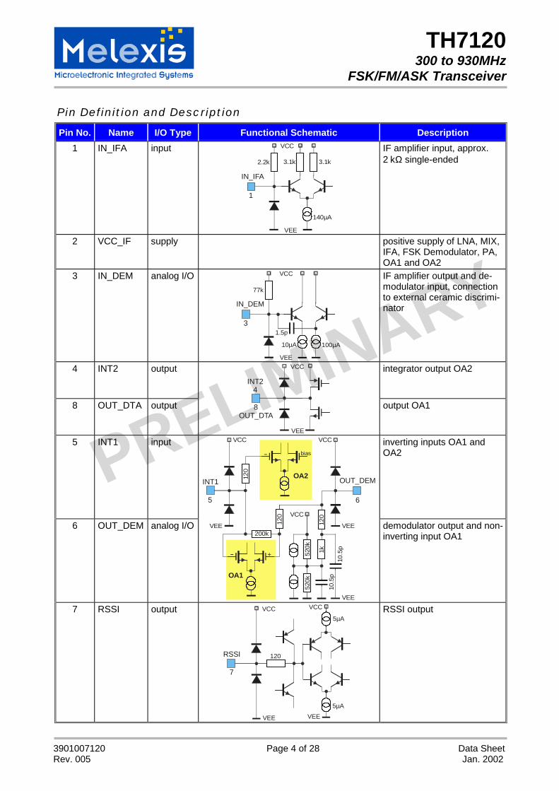
Pin No. Name I/O Type Functional Schematic Description1 IN_IFA input
3.1k3.1k
IN_IFA
1
VCC
140µA
VEE
2.2k
IF amplifier input, approx.2 kΩ single-ended
2 VCC_IF supply positive supply of LNA, MIX,IFA, FSK Demodulator, PA,OA1 and OA2
3 IN_DEM analog I/O
VCC
100µA10µA
VEE
IN_DEM
3
77k
1.5p
IF amplifier output and de-modulator input, connectionto external ceramic discrimi-nator
4 INT2 output integrator output OA2
8 OUT_DTA output
VCC
VEE
INT24
8OUT_DTA
output OA1
5 INT1 input inverting inputs OA1 andOA2
6 OUT_DEM analog I/O
OA2
bias
VEE
VCC
INT1
5
VEE
OUT_DEM
6
VCC
120
120
VEE
VCC
120
10.5
p10
.5p
520k
520k 1k
OA1
+
200kdemodulator output and non-inverting input OA1
7 RSSI output
VCC
VEE
RSSI
7
120
VEE
VCC
5µA
5µA
RSSI output
TH7120300 to 930MHz
FSK/FM/ASK Transceiver
3901007120 Page 5 of 28 Data SheetRev. 005 Jan. 2002
PRELIMINARY
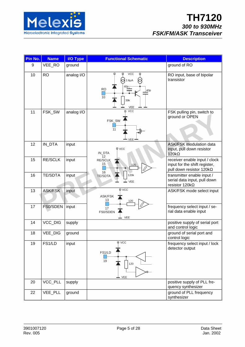
Pin No. Name I/O Type Functional Schematic Description9 VEE_RO ground ground of RO
10 RO analog I/O
40p
VEE
VCC
RO
10
2.6µA
39k
40p
RO input, base of bipolartransistor
11 FSK_SW analog I/O
VCC
VEE
FSK_SW
11
FSK pulling pin, switch toground or OPEN
12 IN_DTA input ASK/FSK modulation datainput, pull down resistor120kΩ
15 RE/SCLK input receiver enable input / clockinput for the shift register,pull down resistor 120kΩ
16 TE/SDTA input VEE
VCCIN_DTA
12RE/SCLK
15
16TE/SDTA 120k
120
transmitter enable input /serial data input, pull downresistor 120kΩ
13 ASK/FSK input ASK/FSK mode select input
17 FS0/SDEN input
VEE
VCC
ASK/FSK13
17FS0/SDEN
120
frequency select input / se-rial data enable input
14 VCC_DIG supply positive supply of serial portand control logic
18 VEE_DIG ground ground of serial port andcontrol logic
19 FS1/LD input
VEE
VCC
FS1/LD
19120
frequency select input / lockdetector output
20 VCC_PLL supply positive supply of PLL fre-quency synthesizer
22 VEE_PLL ground ground of PLL frequencysynthesizer
TH7120300 to 930MHz
FSK/FM/ASK Transceiver
3901007120 Page 6 of 28 Data SheetRev. 005 Jan. 2002
PRELIMINARY
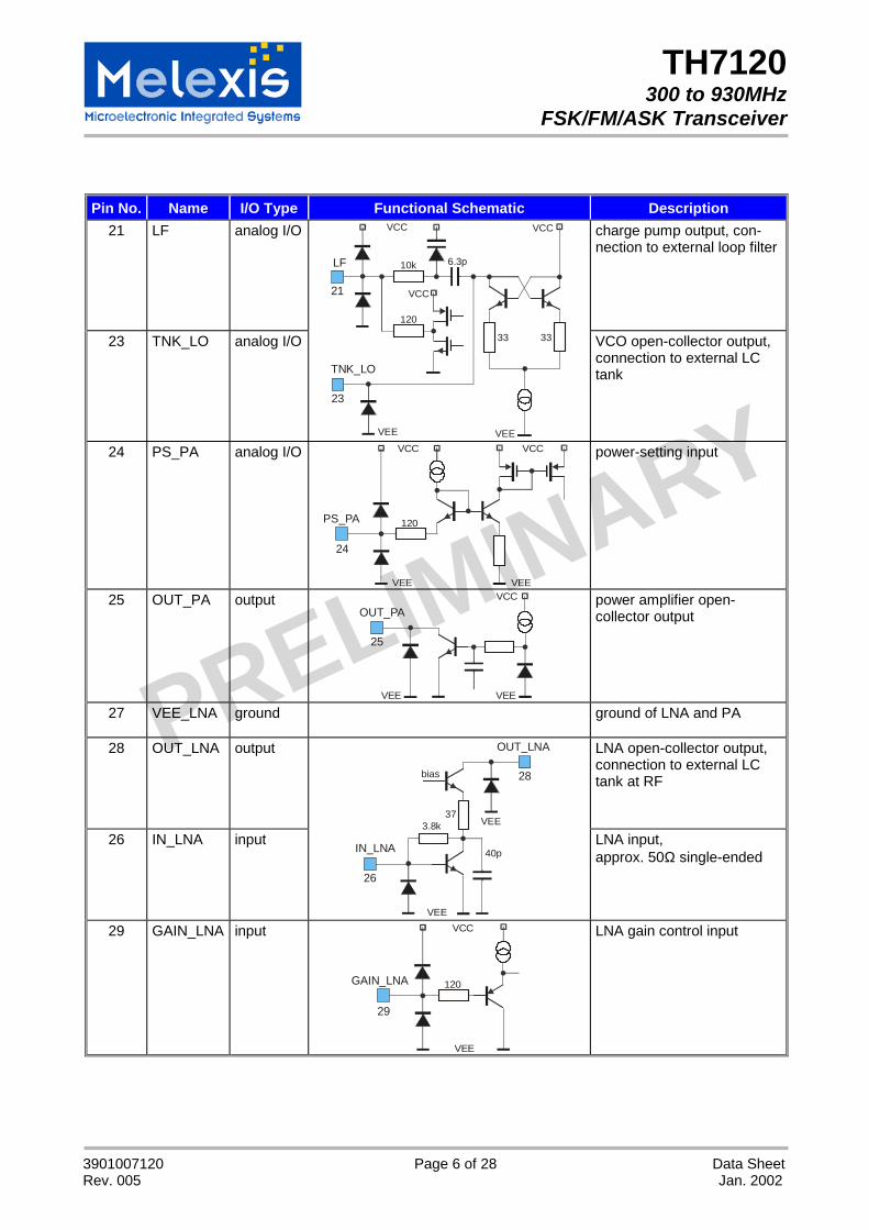
Pin No. Name I/O Type Functional Schematic Description21 LF analog I/O charge pump output, con-
nection to external loop filter
23 TNK_LO analog I/O
120
10k 6.3p
VCC VCC
VCC
VEE
33 33
VEE
LF
21
TNK_LO
23
VCO open-collector output,connection to external LCtank
24 PS_PA analog I/O
VEE VEE
VCC VCC
120PS_PA
24
power-setting input
25 OUT_PA output
VEE VEE
VCCOUT_PA
25
power amplifier open-collector output
27 VEE_LNA ground ground of LNA and PA
28 OUT_LNA output LNA open-collector output,connection to external LCtank at RF
26 IN_LNA input
40p
VEE
VEE3.8k
OUT_LNA
28bias
37
IN_LNA
26
LNA input,approx. 50Ω single-ended
29 GAIN_LNA input
VCC
VEE
GAIN_LNA
29
120
LNA gain control input
TH7120300 to 930MHz
FSK/FM/ASK Transceiver
3901007120 Page 7 of 28 Data SheetRev. 005 Jan. 2002
PRELIMINARY
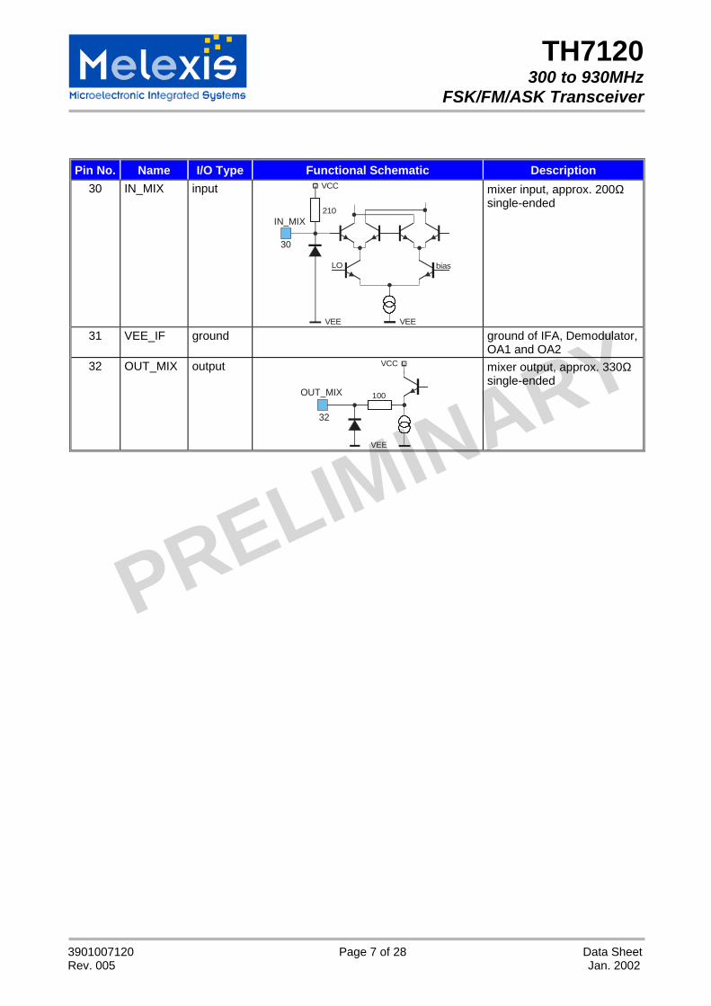
Pin No. Name I/O Type Functional Schematic Description30 IN_MIX input
VCC
210
biasLO
IN_MIX
30
VEE VEE
mixer input, approx. 200Ωsingle-ended
31 VEE_IF ground ground of IFA, Demodulator,OA1 and OA2
32 OUT_MIX output
VCC
VEE
OUT_MIX
32
100
mixer output, approx. 330Ωsingle-ended
TH7120300 to 930MHz
FSK/FM/ASK Transceiver
3901007120 Page 8 of 28 Data SheetRev. 005 Jan. 2002
PRELIMINARY
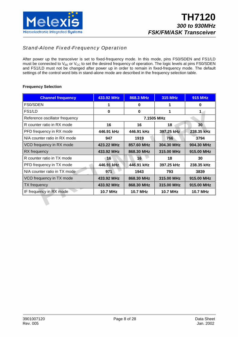
Stand-Alone Fixed-Frequency Operation
After power up the transceiver is set to fixed-frequency mode. In this mode, pins FS0/SDEN and FS1/LDmust be connected to VEE or VCC to set the desired frequency of operation. The logic levels at pins FS0/SDENand FS1/LD must not be changed after power up in order to remain in fixed-frequency mode. The defaultsettings of the control word bits in stand-alone mode are described in the frequency selection table.
Frequency Selection
Channel frequency 433.92 MHz 868.3 MHz 315 MHz 915 MHzFS0/SDEN 1 0 1 0FS1/LD 0 0 1 1Reference oscillator frequency 7.1505 MHzR counter ratio in RX mode 16 16 18 30PFD frequency in RX mode 446.91 kHz 446.91 kHz 397.25 kHz 238.35 kHzN/A counter ratio in RX mode 947 1919 766 3794VCO frequency in RX mode 423.22 MHz 857.60 MHz 304.30 MHz 904.30 MHzRX frequency 433.92 MHz 868.30 MHz 315.00 MHz 915.00 MHzR counter ratio in TX mode 16 16 18 30PFD frequency in TX mode 446.91 kHz 446.91 kHz 397.25 kHz 238.35 kHzN/A counter ratio in TX mode 971 1943 793 3839VCO frequency in TX mode 433.92 MHz 868.30 MHz 315.00 MHz 915.00 MHzTX frequency 433.92 MHz 868.30 MHz 315.00 MHz 915.00 MHzIF frequency in RX mode 10.7 MHz 10.7 MHz 10.7 MHz 10.7 MHz
TH7120300 to 930MHz
FSK/FM/ASK Transceiver
3901007120 Page 9 of 28 Data SheetRev. 005 Jan. 2002
PRELIMINARY
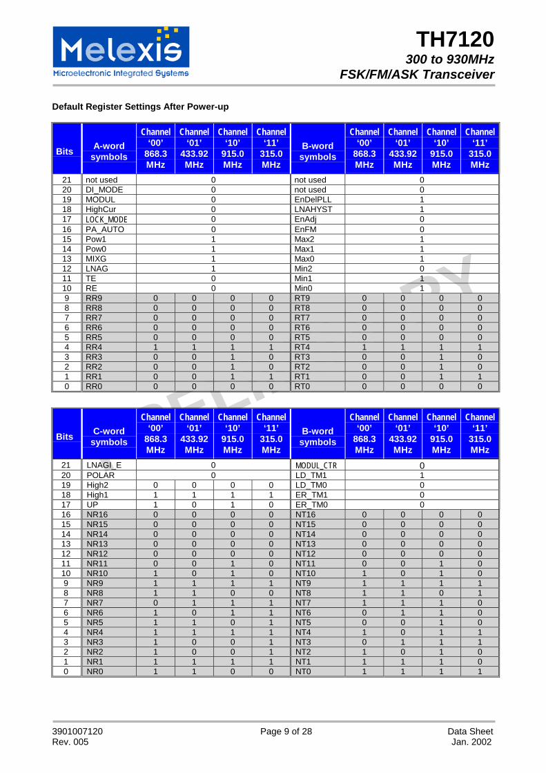
Default Register Settings After Power-up
Bits A-wordsymbols
Channel‘00’
868.3MHz
Channel‘01’
433.92MHz
Channel‘10’
915.0MHz
Channel‘11’
315.0MHz
B-wordsymbols
Channel‘00’
868.3MHz
Channel‘01’
433.92MHz
Channel‘10’
915.0MHz
Channel‘11’
315.0MHz
21 not used 0 not used 020 DI_MODE 0 not used 019 MODUL 0 EnDelPLL 118 HighCur 0 LNAHYST 117 LOCK_MODE 0 EnAdj 016 PA_AUTO 0 EnFM 015 Pow1 1 Max2 114 Pow0 1 Max1 113 MIXG 1 Max0 112 LNAG 1 Min2 011 TE 0 Min1 110 RE 0 Min0 19 RR9 0 0 0 0 RT9 0 0 0 08 RR8 0 0 0 0 RT8 0 0 0 07 RR7 0 0 0 0 RT7 0 0 0 06 RR6 0 0 0 0 RT6 0 0 0 05 RR5 0 0 0 0 RT5 0 0 0 04 RR4 1 1 1 1 RT4 1 1 1 13 RR3 0 0 1 0 RT3 0 0 1 02 RR2 0 0 1 0 RT2 0 0 1 01 RR1 0 0 1 1 RT1 0 0 1 10 RR0 0 0 0 0 RT0 0 0 0 0
Bits C-wordsymbols
Channel‘00’
868.3MHz
Channel‘01’
433.92MHz
Channel‘10’
915.0MHz
Channel‘11’
315.0MHz
B-wordsymbols
Channel‘00’
868.3MHz
Channel‘01’
433.92MHz
Channel‘10’
915.0MHz
Channel‘11’
315.0MHz
21 LNAGI_E 0 MODUL_CTR 020 POLAR 0 LD_TM1 119 High2 0 0 0 0 LD_TM0 018 High1 1 1 1 1 ER_TM1 017 UP 1 0 1 0 ER_TM0 016 NR16 0 0 0 0 NT16 0 0 0 015 NR15 0 0 0 0 NT15 0 0 0 014 NR14 0 0 0 0 NT14 0 0 0 013 NR13 0 0 0 0 NT13 0 0 0 012 NR12 0 0 0 0 NT12 0 0 0 011 NR11 0 0 1 0 NT11 0 0 1 010 NR10 1 0 1 0 NT10 1 0 1 09 NR9 1 1 1 1 NT9 1 1 1 18 NR8 1 1 0 0 NT8 1 1 0 17 NR7 0 1 1 1 NT7 1 1 1 06 NR6 1 0 1 1 NT6 0 1 1 05 NR5 1 1 0 1 NT5 0 0 1 04 NR4 1 1 1 1 NT4 1 0 1 13 NR3 1 0 0 1 NT3 0 1 1 12 NR2 1 0 0 1 NT2 1 0 1 01 NR1 1 1 1 1 NT1 1 1 1 00 NR0 1 1 0 0 NT0 1 1 1 1
TH7120300 to 930MHz
FSK/FM/ASK Transceiver
3901007120 Page 10 of 28 Data SheetRev. 005 Jan. 2002
PRELIMINARY
Programmable Channel Operation
Serial Control Interface Description
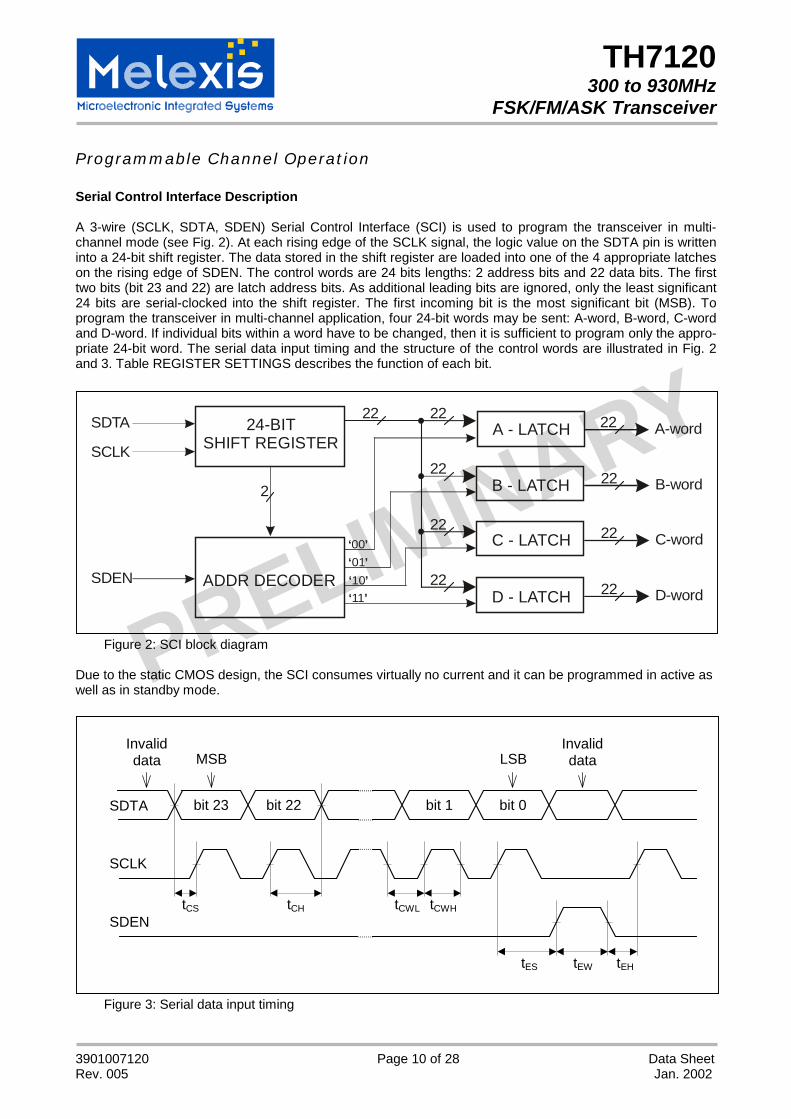
A 3-wire (SCLK, SDTA, SDEN) Serial Control Interface (SCI) is used to program the transceiver in multi-channel mode (see Fig. 2). At each rising edge of the SCLK signal, the logic value on the SDTA pin is writteninto a 24-bit shift register. The data stored in the shift register are loaded into one of the 4 appropriate latcheson the rising edge of SDEN. The control words are 24 bits lengths: 2 address bits and 22 data bits. The firsttwo bits (bit 23 and 22) are latch address bits. As additional leading bits are ignored, only the least significant24 bits are serial-clocked into the shift register. The first incoming bit is the most significant bit (MSB). Toprogram the transceiver in multi-channel application, four 24-bit words may be sent: A-word, B-word, C-wordand D-word. If individual bits within a word have to be changed, then it is sufficient to program only the appro-priate 24-bit word. The serial data input timing and the structure of the control words are illustrated in Fig. 2and 3. Table REGISTER SETTINGS describes the function of each bit.
Figure 2: SCI block diagram
Due to the static CMOS design, the SCI consumes virtually no current and it can be programmed in active aswell as in standby mode.
Figure 3: Serial data input timing
tEHtEWtES
tCWHtCWLtCHtCS
bit 22 bit 1 bit 0bit 23
dataInvalid
LSBMSB
SDTA
SCLK
SDEN
dataInvalid
A - LATCH
ADDR DECODER
B - LATCH
C - LATCH
D - LATCH
22 A-word2222
‘ ’00
‘ ’10‘ ’11
‘ ’01
222
22
22
22 B-word
22 D-word
22 C-word
24-BITSHIFT REGISTER
SDEN
SDTA
SCLK
TH7120300 to 930MHz
FSK/FM/ASK Transceiver
3901007120 Page 11 of 28 Data SheetRev. 005 Jan. 2002
PRELIMINARY
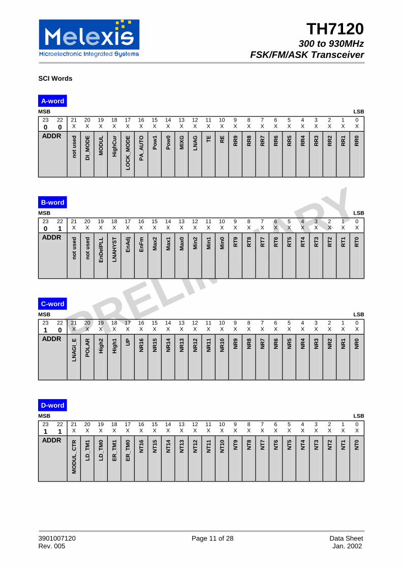
SCI Words
A-word
MSB LSB23 22 21 20 19 18 17 16 15 14 13 12 11 10 9 8 7 6 5 4 3 2 1 00 0 X X X X X X X X X X X X X X X X X X X X X X
ADDR
not u
sed
DI_
MO
DE
MO
DU
L
Hig
hCur
LOC
K_M
OD
E
PA_A
UTO
Pow
1
Pow
0
MIX
G
LNAG TE R
E
RR
9
RR
8
RR
7
RR
6
RR
5
RR
4
RR
3
RR
2
RR
1
RR
0
B-word
MSB LSB23 22 21 20 19 18 17 16 15 14 13 12 11 10 9 8 7 6 5 4 3 2 1 00 1 X X X X X X X X X X X X X X X X X X X X X X
ADDR
not u
sed
not u
sed
EnD
elPL
L
LNAH
YST
EnAd
j
EnFm
Max
2
Max
1
Max
0
Min
2
Min
1
Min
0
RT9
RT8
RT7
RT6
RT5
RT4
RT3
RT2
RT1
RT0
C-word
MSB LSB23 22 21 20 19 18 17 16 15 14 13 12 11 10 9 8 7 6 5 4 3 2 1 01 0 X X X X X X X X X X X X X X X X X X X X X X
ADDR
LNAG
I_E
POLA
R
Hig
h2
Hig
h1 UP
NR
16
NR
15
NR
14
NR
13
NR
12
NR
11
NR
10
NR
9
NR
8
NR
7
NR
6
NR
5
NR
4
NR
3
NR
2
NR
1
NR
0
D-word
MSB LSB23 22 21 20 19 18 17 16 15 14 13 12 11 10 9 8 7 6 5 4 3 2 1 01 1 X X X X X X X X X X X X X X X X X X X X X X
ADDR
MO
DU
L_C
TR
LD_T
M1
LD_T
M0
ER_T
M1
ER_T
M0
NT1
6
NT1
5
NT1
4
NT1
3
NT1
2
NT1
1
NT1
0
NT9
NT8
NT7
NT6
NT5
NT4
NT3
NT2
NT1
NT0
TH7120300 to 930MHz
FSK/FM/ASK Transceiver
3901007120 Page 12 of 28 Data SheetRev. 005 Jan. 2002
PRELIMINARY
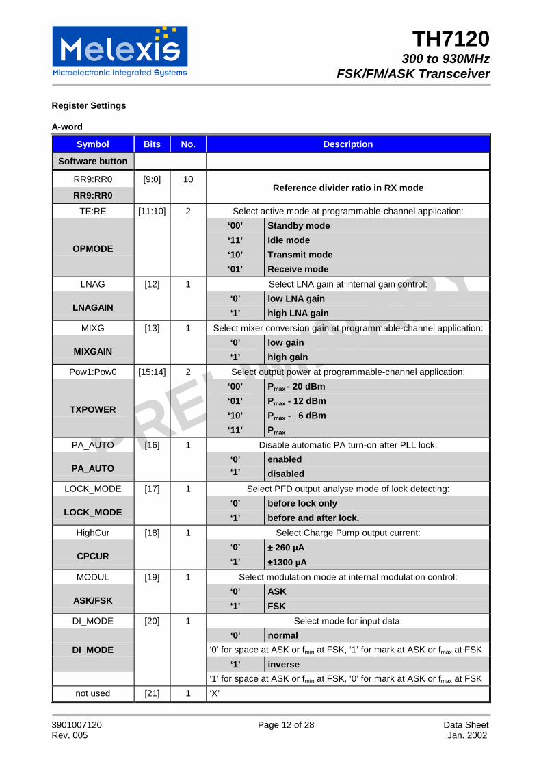
Register Settings
A-word
Symbol Bits No. Description
Software button
RR9:RR0
RR9:RR0
[9:0] 10Reference divider ratio in RX mode
TE:RE [11:10] 2 Select active mode at programmable-channel application:
OPMODE
‘00’‘11’‘10’‘01’
Standby modeIdle modeTransmit modeReceive mode
LNAG [12] 1 Select LNA gain at internal gain control:
LNAGAIN‘0’‘1’
low LNA gainhigh LNA gain
MIXG [13] 1 Select mixer conversion gain at programmable-channel application:
MIXGAIN‘0’‘1’
low gainhigh gain
Pow1:Pow0 [15:14] 2 Select output power at programmable-channel application:
TXPOWER
‘00’‘01’‘10’‘11’
Pmax - 20 dBmPmax - 12 dBmPmax - 6 dBmPmax
PA_AUTO [16] 1 Disable automatic PA turn-on after PLL lock:
PA_AUTO‘0’‘1’
enableddisabled
LOCK_MODE [17] 1 Select PFD output analyse mode of lock detecting:
LOCK_MODE‘0’‘1’
before lock onlybefore and after lock.
HighCur [18] 1 Select Charge Pump output current:
CPCUR‘0’‘1’
±±±± 260 µA±±±±1300 µA
MODUL [19] 1 Select modulation mode at internal modulation control:
ASK/FSK‘0’‘1’
ASKFSK
DI_MODE [20] 1 Select mode for input data:‘0’ normal
DI_MODE ‘0’ for space at ASK or fmin at FSK, ‘1’ for mark at ASK or fmax at FSK‘1’ inverse
‘1’ for space at ASK or fmin at FSK, ‘0’ for mark at ASK or fmax at FSKnot used [21] 1 ‘X’
TH7120300 to 930MHz
FSK/FM/ASK Transceiver
3901007120 Page 13 of 28 Data SheetRev. 005 Jan. 2002
PRELIMINARY
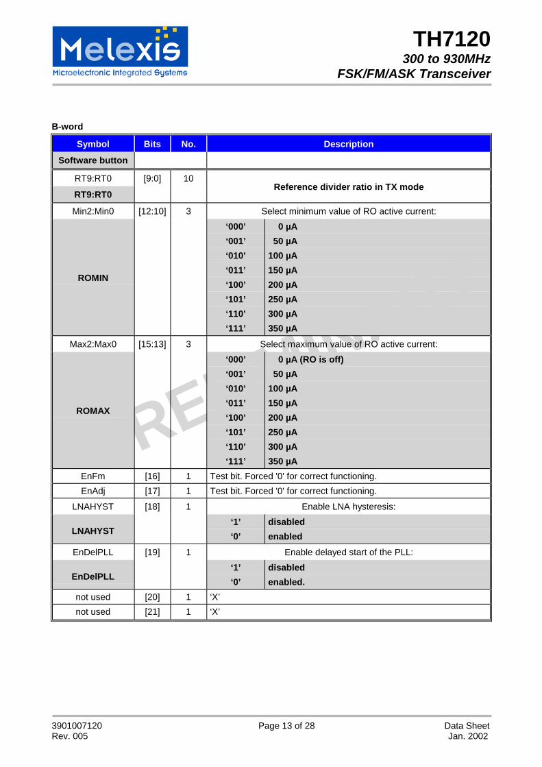
B-word
Symbol Bits No. Description
Software button
RT9:RT0
RT9:RT0
[9:0] 10Reference divider ratio in TX mode
Min2:Min0 [12:10] 3 Select minimum value of RO active current:
ROMIN
‘000’‘001’‘010’‘011’‘100’‘101’‘110’‘111’
0 µA 50 µA100 µA150 µA200 µA250 µA300 µA350 µA
Max2:Max0 [15:13] 3 Select maximum value of RO active current:
ROMAX
‘000’‘001’‘010’‘011’‘100’‘101’‘110’‘111’
0 µA (RO is off) 50 µA100 µA150 µA200 µA250 µA300 µA350 µA
EnFm [16] 1 Test bit. Forced '0' for correct functioning.EnAdj [17] 1 Test bit. Forced '0' for correct functioning.
LNAHYST [18] 1 Enable LNA hysteresis:
LNAHYST‘1’‘0’
disabledenabled
EnDelPLL [19] 1 Enable delayed start of the PLL:
EnDelPLL‘1’‘0’
disabledenabled.
not used [20] 1 ‘X’not used [21] 1 ‘X’
TH7120300 to 930MHz
FSK/FM/ASK Transceiver
3901007120 Page 14 of 28 Data SheetRev. 005 Jan. 2002
PRELIMINARY
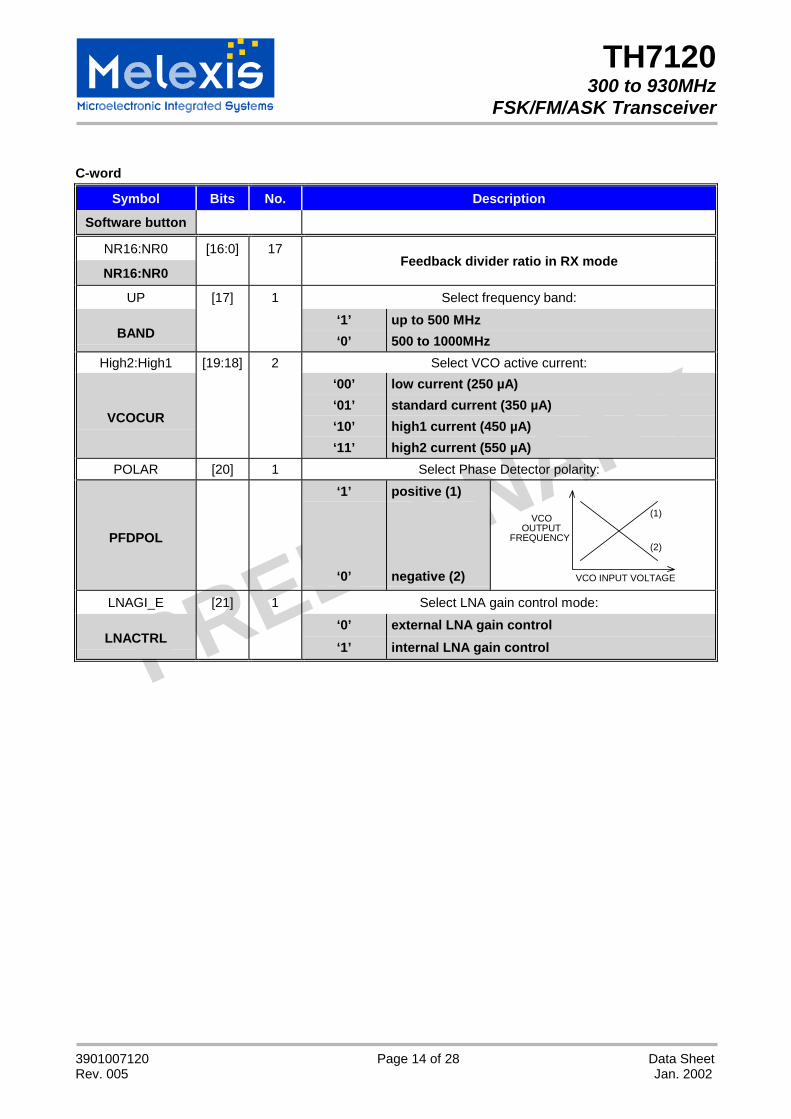
C-word
Symbol Bits No. Description
Software button
NR16:NR0
NR16:NR0
[16:0] 17Feedback divider ratio in RX mode
UP [17] 1 Select frequency band:
BAND‘1’‘0’
up to 500 MHz500 to 1000MHz
High2:High1 [19:18] 2 Select VCO active current:
VCOCUR
‘00’‘01’‘10’‘11’
low current (250 µA)standard current (350 µA)high1 current (450 µA)high2 current (550 µA)
POLAR [20] 1 Select Phase Detector polarity:
PFDPOL
‘1’
‘0’
positive (1)
negative (2)
(2)
(1)
FREQUENCYOUTPUT
VCO
VCO INPUT VOLTAGE
LNAGI_E [21] 1 Select LNA gain control mode:
LNACTRL‘0’‘1’
external LNA gain controlinternal LNA gain control
TH7120300 to 930MHz
FSK/FM/ASK Transceiver
3901007120 Page 15 of 28 Data SheetRev. 005 Jan. 2002
PRELIMINARY
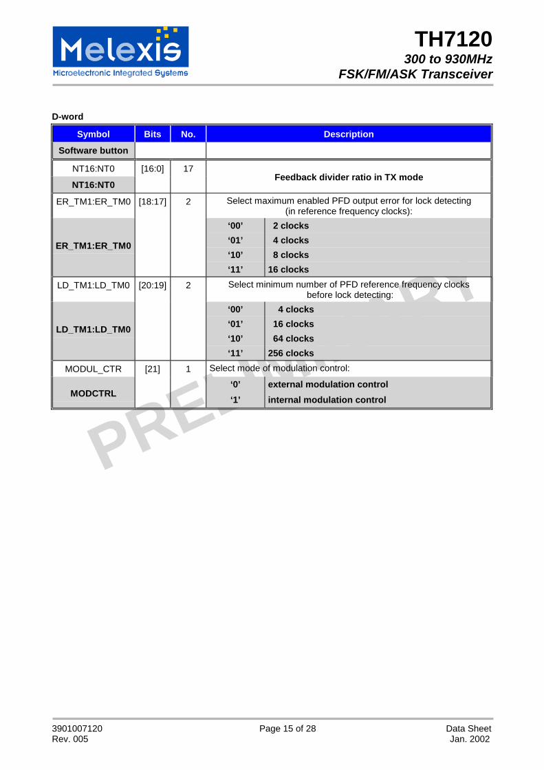
D-word
Symbol Bits No. Description
Software button
NT16:NT0
NT16:NT0
[16:0] 17Feedback divider ratio in TX mode
ER_TM1:ER_TM0 [18:17] 2 Select maximum enabled PFD output error for lock detecting(in reference frequency clocks):
ER_TM1:ER_TM0
‘00’‘01’‘10’‘11’
2 clocks 4 clocks 8 clocks16 clocks
LD_TM1:LD_TM0 [20:19] 2 Select minimum number of PFD reference frequency clocks before lock detecting:
LD_TM1:LD_TM0
‘00’‘01’‘10’‘11’
4 clocks 16 clocks 64 clocks256 clocks
MODUL_CTR [21] 1 Select mode of modulation control:
MODCTRL‘0’‘1’
external modulation controlinternal modulation control
TH7120300 to 930MHz
FSK/FM/ASK Transceiver
3901007120 Page 16 of 28 Data SheetRev. 005 Jan. 2002
PRELIMINARY
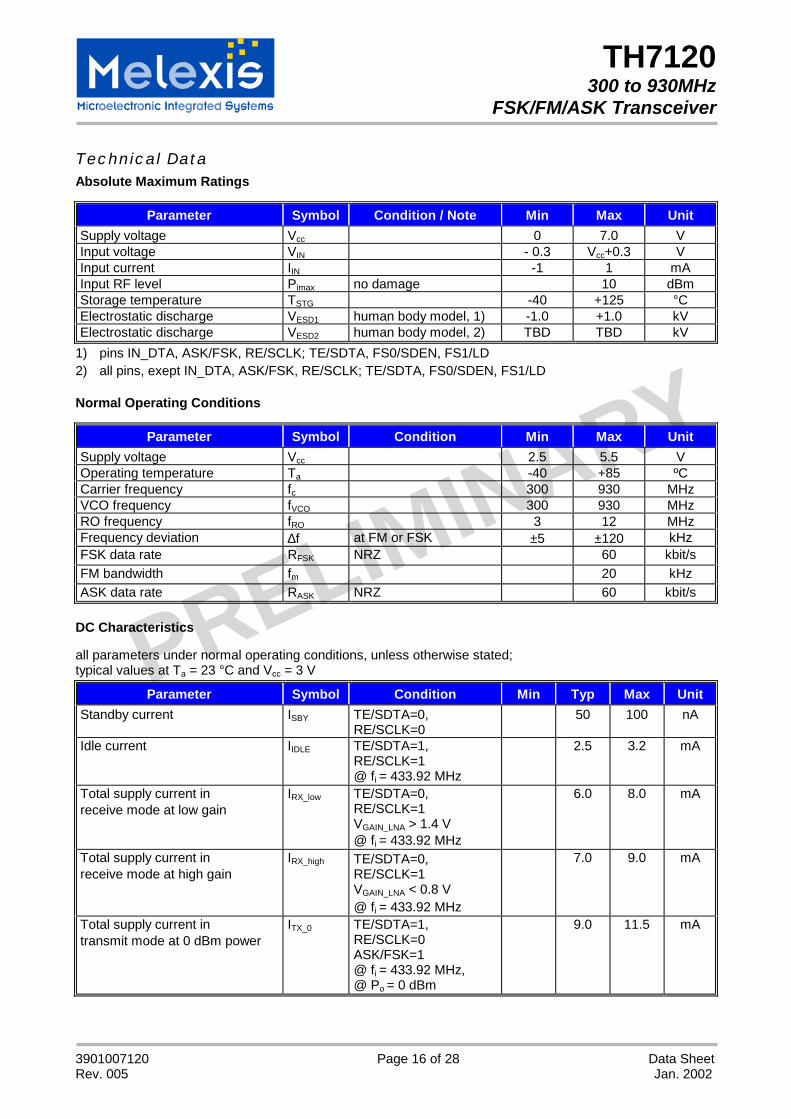
Technical DataAbsolute Maximum Ratings
Parameter Symbol Condition / Note Min Max Unit Supply voltage Vcc 0 7.0 V Input voltage VIN - 0.3 Vcc+0.3 V Input current IIN -1 1 mA Input RF level Pimax no damage 10 dBm Storage temperature TSTG -40 +125 °C Electrostatic discharge VESD1 human body model, 1) -1.0 +1.0 kV Electrostatic discharge VESD2 human body model, 2) TBD TBD kV
1) pins IN_DTA, ASK/FSK, RE/SCLK; TE/SDTA, FS0/SDEN, FS1/LD2) all pins, exept IN_DTA, ASK/FSK, RE/SCLK; TE/SDTA, FS0/SDEN, FS1/LD
Normal Operating Conditions
Parameter Symbol Condition Min Max Unit Supply voltage Vcc 2.5 5.5 V Operating temperature Ta -40 +85 ºC Carrier frequency fc 300 930 MHzVCO frequency fVCO 300 930 MHzRO frequency fRO 3 12 MHzFrequency deviation ∆f at FM or FSK ±5 ±120 kHzFSK data rate RFSK NRZ 60 kbit/sFM bandwidth fm 20 kHzASK data rate RASK NRZ 60 kbit/s
DC Characteristics
all parameters under normal operating conditions, unless otherwise stated;typical values at Ta = 23 °C and Vcc = 3 V
Parameter Symbol Condition Min Typ Max UnitStandby current ISBY TE/SDTA=0,
RE/SCLK=050 100 nA
Idle current IIDLE TE/SDTA=1,RE/SCLK=1@ fi = 433.92 MHz
2.5 3.2 mA
Total supply current inreceive mode at low gain
IRX_low TE/SDTA=0,RE/SCLK=1VGAIN_LNA > 1.4 V@ fi = 433.92 MHz
6.0 8.0 mA
Total supply current inreceive mode at high gain
IRX_high TE/SDTA=0,RE/SCLK=1VGAIN_LNA < 0.8 V@ fi = 433.92 MHz
7.0 9.0 mA
Total supply current intransmit mode at 0 dBm power
ITX_0 TE/SDTA=1,RE/SCLK=0ASK/FSK=1@ fi = 433.92 MHz,@ Po = 0 dBm
9.0 11.5 mA
TH7120300 to 930MHz
FSK/FM/ASK Transceiver
3901007120 Page 17 of 28 Data SheetRev. 005 Jan. 2002
PRELIMINARY
AC System Characteristics of the Receiver Part
all parameters under normal operating conditions, unless otherwise stated; all parameters based on testcircuits for FSK (Fig. 4 to 5), FM and ASK (Fig. 6 to 7), respectively; RF at 433.92 MHz
Parameter Symbol Condition Min Typ Max UnitInput sensitivity – FSK Pmin_FSK BIF = 150kHz
∆f = ± 50 kHz (FSK/FM)BER ≤ 3⋅10-3
-103 dBm
Input sensitivity – ASK Pmin_ASK BIF = 150kHzBER ≤ 3⋅10-3
-105 dBm
Maximum input signal – FSK/FMat low gain
Pmax_FSK_1 BER ≤ 3⋅10-3
VGAIN_LNA > 1.4 V10 dBm
Maximum input signal – FSK/FMat high gain
Pmax_FSK_0 BER ≤ 3⋅10-3
VGAIN_LNA < 0.8 V-10 dBm
Maximum input signal – ASKat low gain
Pmax_ASK_1 BER ≤ 3⋅10-3
VGAIN_LNA > 1.4 V-20 dBm
Maximum input signal – ASKat high gain
Pmax_ASK_0 BER ≤ 3⋅10-3
VGAIN_LNA < 0.8 V0 dBm
Image rejection ∆Pimag TBD dBBlocking immunity ∆Pblock ∆fblock > ±2MHz, note 1 TBD dBStart-up time – FSK/FM TFSK TE/SDTA=0,
RE/SCLK=1valid data at output
1 ms
Start-up time – ASK TASK depends on ASK de-tector time constant andstart-up mode, validdata at output
TFSK+
200K * C6
ms
Spurious emission Pspur -70 dBmNotes: 1. desired signal with FSK/FM or ASK modulation, CW blocking signal
AC System Characteristics of the Transmitter Part
all parameters under normal operating conditions, unless otherwise stated;typical values at Ta = 23 °C and Vcc = 3 V;TE/SDTA=1, RE/SCLK=0, ASK/FSK=1, RPS≥15 kΩ, fc = 433.92 MHz, test circuit shown in Fig. 4 to 7
Parameter Symbol Condition Min Typ Max UnitOutput power Po CW mode 4 6 8 dBmFSK deviation ∆fFSK depends on Cx1, Cx2 and
crystal parameter±5 ±50 ±100 kHz
Data rate FSK RFSK 60 kbit/sFM deviation ∆fFM adjustable with varactor
and VFM
±6 kHz
Modulation frequency FM fmod 5 kHzData rate ASK RASK 60 kbit/sPLL spurs emission Pspur at all fc and nominal Po -36 dBmHarmonic emission Pharm at all fc and power steps - -36 dBmVCO gain KVCO 35 MHz/VCharge pump current ICP 260 µAStart-up time TTX from ”standby” to
“transmit” mode1 ms
TH7120300 to 930MHz
FSK/FM/ASK Transceiver
3901007120 Page 18 of 28 Data SheetRev. 005 Jan. 2002
PRELIMINARY
Output Power Selection
typical values at Ta = 23 °C and Vcc = 3 V:TE/SDTA = 1, RE/SCLK = 0, ASK/FSK = 1, fc = 433.92 MHz, CW mode
RPS / kΩΩΩΩ ≥≥≥≥ 15 k 6.8 k 3.3 k 1.0 k
ICC / mA TBD 9.0 TBD TBDPO / dBm 6 0 -6 -15
Pharm / dBm ≤-36 ≤-36 ≤-36 ≤-36
Serial Control Interface
Parameter Symbol Condition Min Max Unit
Data to clock set up time fCS 150 ns
Data to clock hold time tCH 50 ns
Clock pulse width high tCWH 100 ns
Clock pulse width low tCWL 100 ns
Clock to load enable setup time
tES 100
Crystal Parameters
Parameter Symbol Condition Min Max Unit
Crystal frequency fcrystal fundamental mode, AT 3 12 MHz
Load capacitance Cload 10 15 pF
Static capacitance C0 7 pF
Motional resistance Rm 70 Ω
TH7120300 to 930MHz
FSK/FM/ASK Transceiver
3901007120 Page 19 of 28 Data SheetRev. 005 Jan. 2002
PRELIMINARY
Application Circuit Examples
Programmable Channel FSK Application Circuit
Figure 4: Test circuit for programmable channel FSK operation
SCLK
SDTA
SDEN
Lockdetect
FSKoutput
FSKinput
CX1
CX2
CERFIL
XTAL
RPS
RB
CTX0
C1
C2
L1
LTX0
CRX0
L0
RSSI
OUT_MIX
VEE
CER
RES
C3CB5
C5C4
C0
CB0
CB1
CB2
CB3
CB6
CB7RE/SCLK
IN_DTA
ASK/FSK
FSK_SW
RO
VCC
VEE
VCC
FS1/
LD
VEELF
TNK_
LO
OUT_PA
IN_LNA
OUT_LNA
VEE
GAIN_LNA
IN_MIX
VEE
IN_I
FA
IN_D
EM
INT2
INT1
RSS
I
OU
T_D
EM
OU
T_D
TA
VCC
VCC
VCC
VCC
VCC
FS0/
SDEN
CB4
RF inputRF output
Antennamatchingnetwork
CP0RP
CF1CF2
RF
TH7120300 to 930MHz
FSK/FM/ASK Transceiver
3901007120 Page 20 of 28 Data SheetRev. 005 Jan. 2002
PRELIMINARY
Fixed-Frequency FSK Application Circuit
Figure 5: Test circuit for fixed-frequency FSK operation at 433 MHz
FSKoutput
FSKinput
TXenable
RXenable
CX1
CX2
XTAL
RPS
RB
CTX0
C1
C2
L1
LTX0
CRX0
L0
CERFILRSSI
OUT_MIX
VEE
CB5
C5C4
C0
CF1CF2
RF
CB4 CB0
CB1
CB2
CB3
CB6
CB7
C3
RF inputRF output
Antennamatchingnetwork
CER
RES
CP0RP
RE/SCLK
IN_DTA
ASK/FSK
FSK_SW
RO
VCC
VEE
VCC
FS1/
LD
VEELF
TNK_
LO
OUT_PA
IN_LNA
OUT_LNA
VEE
GAIN_LNA
IN_MIX
VEE
IN_I
FA
IN_D
EM
INT2
INT1
RSS
I
OU
T_D
EM
OU
T_D
TA
VCC
VCC
VCC
VCC
VCC
FS0/
SDEN
TH7120300 to 930MHz
FSK/FM/ASK Transceiver
3901007120 Page 21 of 28 Data SheetRev. 005 Jan. 2002
PRELIMINARY
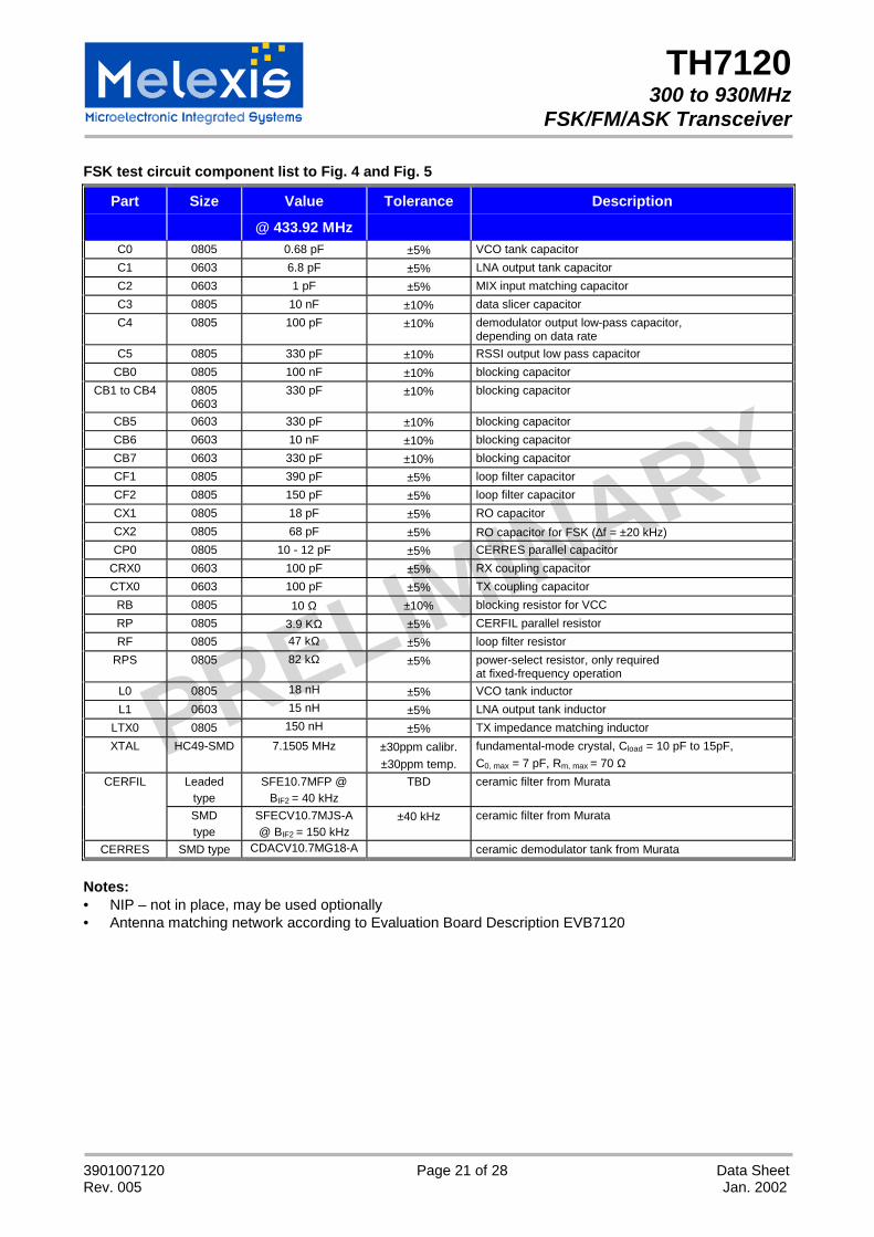
FSK test circuit component list to Fig. 4 and Fig. 5
Part Size Value
@ 433.92 MHz
Tolerance Description
C0 0805 0.68 pF ±5% VCO tank capacitorC1 0603 6.8 pF ±5% LNA output tank capacitorC2 0603 1 pF ±5% MIX input matching capacitorC3 0805 10 nF ±10% data slicer capacitorC4 0805 100 pF ±10% demodulator output low-pass capacitor,
depending on data rateC5 0805 330 pF ±10% RSSI output low pass capacitor
CB0 0805 100 nF ±10% blocking capacitorCB1 to CB4 0805
0603330 pF ±10% blocking capacitor
CB5 0603 330 pF ±10% blocking capacitorCB6 0603 10 nF ±10% blocking capacitorCB7 0603 330 pF ±10% blocking capacitorCF1 0805 390 pF ±5% loop filter capacitorCF2 0805 150 pF ±5% loop filter capacitorCX1 0805 18 pF ±5% RO capacitorCX2 0805 68 pF ±5% RO capacitor for FSK (∆f = ±20 kHz)CP0 0805 10 - 12 pF ±5% CERRES parallel capacitor
CRX0 0603 100 pF ±5% RX coupling capacitorCTX0 0603 100 pF ±5% TX coupling capacitor
RB 0805 10 Ω ±10% blocking resistor for VCCRP 0805 3.9 KΩ ±5% CERFIL parallel resistorRF 0805 47 kΩ ±5% loop filter resistor
RPS 0805 82 kΩ ±5% power-select resistor, only requiredat fixed-frequency operation
L0 0805 18 nH ±5% VCO tank inductorL1 0603 15 nH ±5% LNA output tank inductor
LTX0 0805 150 nH ±5% TX impedance matching inductorXTAL HC49-SMD 7.1505 MHz ±30ppm calibr.
±30ppm temp.fundamental-mode crystal, Cload = 10 pF to 15pF,C0, max = 7 pF, Rm, max = 70 Ω
CERFIL Leadedtype
SFE10.7MFP @BIF2 = 40 kHz
TBD ceramic filter from Murata
SMDtype
SFECV10.7MJS-A@ BIF2 = 150 kHz
±40 kHz ceramic filter from Murata
CERRES SMD type CDACV10.7MG18-A ceramic demodulator tank from Murata
Notes:• NIP – not in place, may be used optionally• Antenna matching network according to Evaluation Board Description EVB7120
TH7120300 to 930MHz
FSK/FM/ASK Transceiver
3901007120 Page 22 of 28 Data SheetRev. 005 Jan. 2002
PRELIMINARY
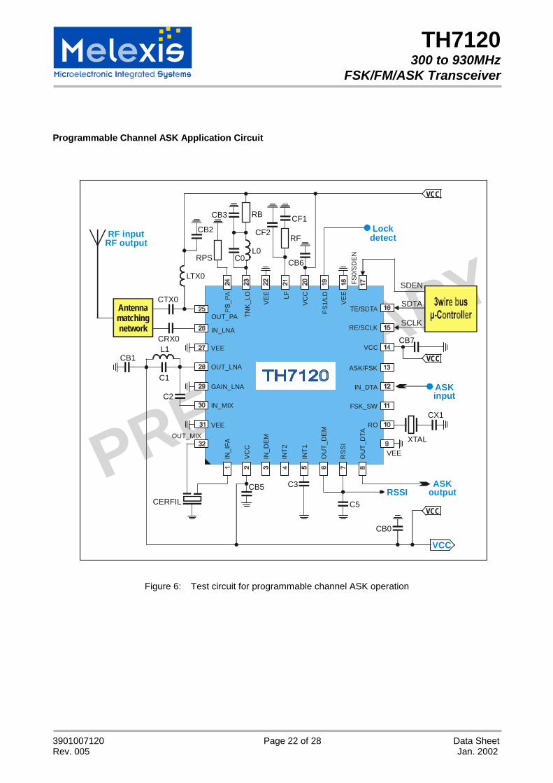
Programmable Channel ASK Application Circuit
Figure 6: Test circuit for programmable channel ASK operation
ASKoutput
ASKinput
CX1
CERFIL
XTAL
RPS
RB
CTX0
C1
C2
L1
LTX0
CRX0
L0
RSSI
OUT_MIX
VEE
C3CB5
C5
C0
CB0
CB1
CB2
CB3
CB6
CB7RE/SCLK
IN_DTA
ASK/FSK
FSK_SW
RO
VCC
VEE
VCC
FS1/
LD
VEELF
TNK_
LO
OUT_PA
IN_LNA
OUT_LNA
VEE
GAIN_LNA
IN_MIX
VEE
IN_I
FA
IN_D
EM
INT2
INT1
RSS
I
OU
T_D
EM
OU
T_D
TA
VCC
VCC
VCC
VCC
VCC
SCLK
SDTA
SDEN
Lockdetect
FS0/
SDEN
RF inputRF output
Antennamatchingnetwork
CF1CF2
RF
TH7120300 to 930MHz
FSK/FM/ASK Transceiver
3901007120 Page 23 of 28 Data SheetRev. 005 Jan. 2002
PRELIMINARY
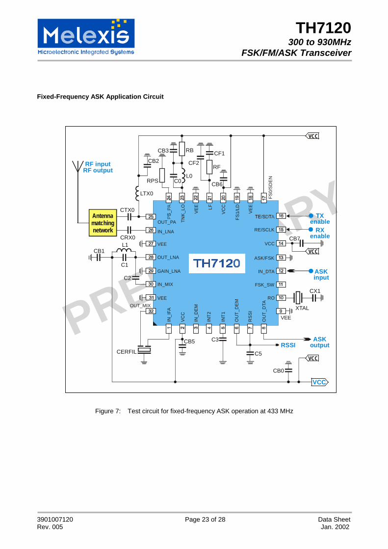
Fixed-Frequency ASK Application Circuit
Figure 7: Test circuit for fixed-frequency ASK operation at 433 MHz
ASKoutput
ASKinput
TXenable
RXenable
CX1
CERFIL
XTAL
RPS
RB
CTX0
C1
C2
L1
LTX0
CRX0
L0
RSSI
OUT_MIX
VEE
C3CB5
C5
C0
CB0
CB1
CB2
CB3
CB6
CB7RE/SCLK
IN_DTA
ASK/FSK
FSK_SW
RO
VCC
VEE
VCC
FS1/
LD
VEELF
TNK_
LO
OUT_PA
IN_LNA
OUT_LNA
VEE
GAIN_LNA
IN_MIX
VEE
IN_I
FA
IN_D
EM
INT2
INT1
RSS
I
OU
T_D
EM
OU
T_D
TA
VCC
VCC
VCC
VCC
VCC
FS0/
SDEN
RF inputRF output
Antennamatchingnetwork
CF1CF2
RF
TH7120300 to 930MHz
FSK/FM/ASK Transceiver
3901007120 Page 24 of 28 Data SheetRev. 005 Jan. 2002
PRELIMINARY
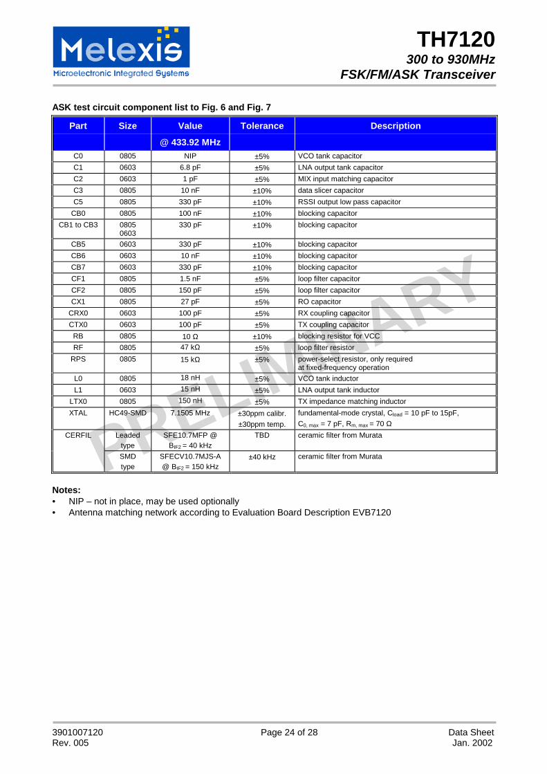
ASK test circuit component list to Fig. 6 and Fig. 7
Part Size Value
@ 433.92 MHz
Tolerance Description
C0 0805 NIP ±5% VCO tank capacitorC1 0603 6.8 pF ±5% LNA output tank capacitorC2 0603 1 pF ±5% MIX input matching capacitorC3 0805 10 nF ±10% data slicer capacitorC5 0805 330 pF ±10% RSSI output low pass capacitor
CB0 0805 100 nF ±10% blocking capacitorCB1 to CB3 0805
0603330 pF ±10% blocking capacitor
CB5 0603 330 pF ±10% blocking capacitorCB6 0603 10 nF ±10% blocking capacitorCB7 0603 330 pF ±10% blocking capacitorCF1 0805 1.5 nF ±5% loop filter capacitorCF2 0805 150 pF ±5% loop filter capacitorCX1 0805 27 pF ±5% RO capacitor
CRX0 0603 100 pF ±5% RX coupling capacitorCTX0 0603 100 pF ±5% TX coupling capacitor
RB 0805 10 Ω ±10% blocking resistor for VCCRF 0805 47 kΩ ±5% loop filter resistor
RPS 0805 15 kΩ ±5% power-select resistor, only requiredat fixed-frequency operation
L0 0805 18 nH ±5% VCO tank inductorL1 0603 15 nH ±5% LNA output tank inductor
LTX0 0805 150 nH ±5% TX impedance matching inductorXTAL HC49-SMD 7.1505 MHz ±30ppm calibr.
±30ppm temp.fundamental-mode crystal, Cload = 10 pF to 15pF,C0, max = 7 pF, Rm, max = 70 Ω
CERFIL Leadedtype
SFE10.7MFP @BIF2 = 40 kHz
TBD ceramic filter from Murata
SMDtype
SFECV10.7MJS-A@ BIF2 = 150 kHz
±40 kHz ceramic filter from Murata
Notes:• NIP – not in place, may be used optionally• Antenna matching network according to Evaluation Board Description EVB7120
TH7120300 to 930MHz
FSK/FM/ASK Transceiver
3901007120 Page 25 of 28 Data SheetRev. 005 Jan. 2002
PRELIMINARY
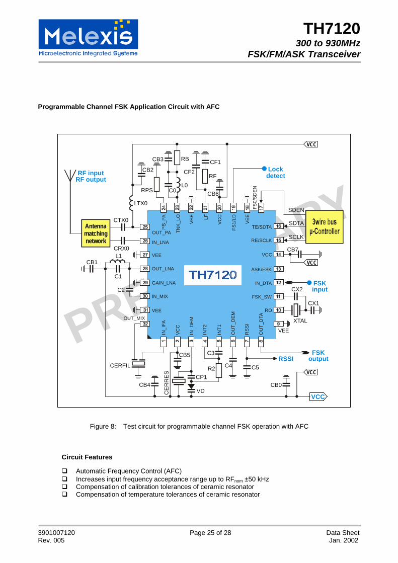
Programmable Channel FSK Application Circuit with AFC
Figure 8: Test circuit for programmable channel FSK operation with AFC
Circuit Features
! Automatic Frequency Control (AFC)! Increases input frequency acceptance range up to RFnom ±50 kHz! Compensation of calibration tolerances of ceramic resonator! Compensation of temperature tolerances of ceramic resonator
VD
FSKoutput
FSKinput
CX1
CX2
CERFIL
XTAL
RPS
RB
CTX0
C1
C2
L1
LTX0
CRX0
L0
RSSI
OUT_MIX
VEE
CER
RES
C3CB5
R2 C5C4
C0
CB0
CB1
CB2
CB3
CB6
CP1
RE/SCLK
IN_DTA
ASK/FSK
FSK_SW
RO
VCC
VEE
VCC
FS1/
LD
VEELF
TNK_
LO
OUT_PA
IN_LNA
OUT_LNA
VEE
GAIN_LNA
IN_MIX
VEE
IN_I
FA
IN_D
EM
INT2
INT1
RSS
I
OU
T_D
EM
OU
T_D
TA
VCC
VCC
VCC
VCC
SCLK
SDTA
SDEN
Lockdetect
FS0/
SDEN
CB4
RF inputRF output
Antennamatchingnetwork
CB7
VCC
CF1CF2
RF
TH7120300 to 930MHz
FSK/FM/ASK Transceiver
3901007120 Page 26 of 28 Data SheetRev. 005 Jan. 2002
PRELIMINARY
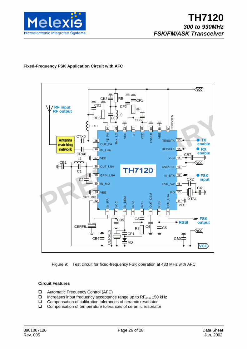
Fixed-Frequency FSK Application Circuit with AFC
Figure 9: Test circuit for fixed-frequency FSK operation at 433 MHz with AFC
Circuit Features
! Automatic Frequency Control (AFC)! Increases input frequency acceptance range up to RFnom ±50 kHz! Compensation of calibration tolerances of ceramic resonator! Compensation of temperature tolerances of ceramic resonator
VD
FSKoutput
FSKinput
TXenable
RXenable
CX1
CX2
CERFIL
XTAL
RPS
RB
CTX0
C1
C2
L1
LTX0
CRX0
L0
RSSI
FS0/
SDEN
OUT_MIX
VEE
CER
RES
C3CB5
R2 C5C4
C0
CB0
CB1
CB2
CB3
CB6
CB7
CP1
RE/SCLK
IN_DTA
ASK/FSK
FSK_SW
RO
VCC
VEE
VCC
FS1/
LD
VEELF
TNK_
LO
OUT_PA
IN_LNA
OUT_LNA
VEE
GAIN_LNA
IN_MIX
VEE
IN_I
FA
IN_D
EM
INT2
INT1
RSS
I
OU
T_D
EM
OU
T_D
TA
VCC
VCC
VCC
VCC
VCC
CB4
RF inputRF output
Antennamatchingnetwork
CF1CF2
RF
TH7120300 to 930MHz
FSK/FM/ASK Transceiver
3901007120 Page 27 of 28 Data SheetRev. 005 Jan. 2002
PRELIMINARY
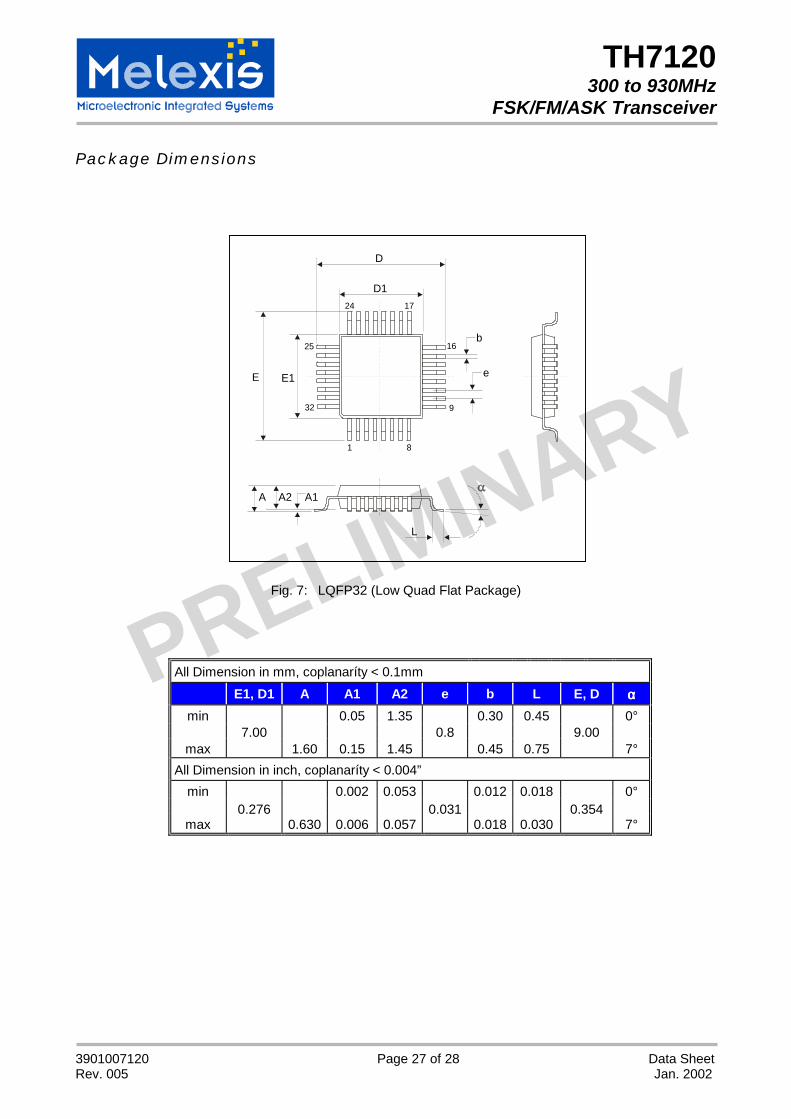
Package Dimensions
Fig. 7: LQFP32 (Low Quad Flat Package)
All Dimension in mm, coplanaríty < 0.1mmE1, D1 A A1 A2 e b L E, D αααα
min 0.05 1.35 0.30 0.45 0°7.00 0.8 9.00
max 1.60 0.15 1.45 0.45 0.75 7°All Dimension in inch, coplanaríty < 0.004”
min 0.002 0.053 0.012 0.018 0°0.276 0.031 0.354
max 0.630 0.006 0.057 0.018 0.030 7°
A1A2A
b
e
1
32
25
1724
8
9
16
D
D1
E1E
L
TH7120300 to 930MHz
FSK/FM/ASK Transceiver
3901007120 Page 28 of 28 Data SheetRev. 005 Jan. 2002
PRELIMINARY
Your Notes
Important Notice
Devices sold by Melexis are covered by the warranty and patent indemnification provisions appearing in its Term of Sale. Melexis makes no warranty, ex-press, statutory, implied, or by description regarding the information set forth herein or regarding the freedom of the described devices from patent infringe-ment. Melexis reserves the right to change specifications and prices at any time and without notice. Therefore, prior to designing this product into a system, itis necessary to check with Melexis for current information. This product is intended for use in normal commercial applications. Applications requiring ex-tended temperature range, unusual environmental requirements, or high reliability applications, such as military, medical life-support or life-sustaining equip-ment are specifically not recommended without additional processing by Melexis for each application.The information furnished by Melexis is believed to be correct and accurate. However, Melexis shall not be liable to recipient or any third party for any dam-ages, including but not limited to personal injury, property damage, loss of profits, loss of use, interrupt of business or indirect, special incidental or conse-quential damages, of any kind, in connection with or arising out of the furnishing, performance or use of the technical data herein. No obligation or liability torecipient or any third party shall arise or flow out of Melexis’ rendering of technical or other services.© 2000 Melexis GmbH. All rights reserved.
For the latest version of this document. Go to our website atwww.melexis.com
Or for additional information contact Melexis Direct:
Europe and Japan: All other locations:Phone: +32 1361 1631 Phone: +1 603 223 2362
QS9000, VDA6.1 and ISO14001 Certified
This datasheet has been downloaded from:
www.DatasheetCatalog.com
Datasheets for electronic components.
Related Documents