October 2016 DocID022138 Rev 5 1/67 1 UM1461 User manual STM3240G-EVAL evaluation board Introduction The STM3240G-EVAL evaluation board is a complete demonstration and development platform for the STM32F4 Series and includes an embedded STM32F407IGH6 high- performance ARM ® Cortex ® -M4F 32-bit microcontroller. The full range of hardware features provided on the board is described to evaluate all peripherals (USB-OTG HS, USB-OTG FS, Ethernet, motor control, CAN, microSD™ card, smartcard, USART, Audio DAC, RS-232, IrDA up to version C07 of the board, SRAM, ST MEMS, EEPROM etc.) before developing applications. Extension headers are used to easily connect a daughterboard or a wrapping board for any specific application. The in-circuit ST-LINK/V2 tool provides easy JTAG and SWD interface debugging and programming. Figure 1. STM3240G-EVAL evaluation board 1. Picture is not contractual www.st.com

Welcome message from author
This document is posted to help you gain knowledge. Please leave a comment to let me know what you think about it! Share it to your friends and learn new things together.
Transcript

October 2016 DocID022138 Rev 5 1/67
1
UM1461User manual
STM3240G-EVAL evaluation board
Introduction
The STM3240G-EVAL evaluation board is a complete demonstration and development platform for the STM32F4 Series and includes an embedded STM32F407IGH6 high-performance ARM®Cortex®-M4F 32-bit microcontroller.
The full range of hardware features provided on the board is described to evaluate all peripherals (USB-OTG HS, USB-OTG FS, Ethernet, motor control, CAN, microSD™ card, smartcard, USART, Audio DAC, RS-232, IrDA up to version C07 of the board, SRAM, ST MEMS, EEPROM etc.) before developing applications. Extension headers are used to easily connect a daughterboard or a wrapping board for any specific application.
The in-circuit ST-LINK/V2 tool provides easy JTAG and SWD interface debugging and programming.
Figure 1. STM3240G-EVAL evaluation board
1. Picture is not contractual
www.st.com
Contents UM1461
2/67 DocID022138 Rev 5
Contents
1 Overview . . . . . . . . . . . . . . . . . . . . . . . . . . . . . . . . . . . . . . . . . . . . . . . . . . 6
1.1 Features . . . . . . . . . . . . . . . . . . . . . . . . . . . . . . . . . . . . . . . . . . . . . . . . . . . 6
1.2 Demonstration software . . . . . . . . . . . . . . . . . . . . . . . . . . . . . . . . . . . . . . . 6
1.3 Ordering information . . . . . . . . . . . . . . . . . . . . . . . . . . . . . . . . . . . . . . . . . . 7
1.4 Delivery recommendations . . . . . . . . . . . . . . . . . . . . . . . . . . . . . . . . . . . . . 7
2 Hardware layout and configuration . . . . . . . . . . . . . . . . . . . . . . . . . . . . . 7
2.1 Power supply . . . . . . . . . . . . . . . . . . . . . . . . . . . . . . . . . . . . . . . . . . . . . . 10
2.2 Boot option . . . . . . . . . . . . . . . . . . . . . . . . . . . . . . . . . . . . . . . . . . . . . . . . .11
2.3 Clock source . . . . . . . . . . . . . . . . . . . . . . . . . . . . . . . . . . . . . . . . . . . . . . . 12
2.4 Reset source . . . . . . . . . . . . . . . . . . . . . . . . . . . . . . . . . . . . . . . . . . . . . . 12
2.5 Audio . . . . . . . . . . . . . . . . . . . . . . . . . . . . . . . . . . . . . . . . . . . . . . . . . . . . 12
2.6 EEPROM . . . . . . . . . . . . . . . . . . . . . . . . . . . . . . . . . . . . . . . . . . . . . . . . . 13
2.7 CAN . . . . . . . . . . . . . . . . . . . . . . . . . . . . . . . . . . . . . . . . . . . . . . . . . . . . . 13
2.8 RS-232 and IrDA . . . . . . . . . . . . . . . . . . . . . . . . . . . . . . . . . . . . . . . . . . . 14
2.9 Motor control . . . . . . . . . . . . . . . . . . . . . . . . . . . . . . . . . . . . . . . . . . . . . . 15
2.10 Smartcard . . . . . . . . . . . . . . . . . . . . . . . . . . . . . . . . . . . . . . . . . . . . . . . . . 16
2.11 microSD card . . . . . . . . . . . . . . . . . . . . . . . . . . . . . . . . . . . . . . . . . . . . . . 16
2.12 ST MEMS . . . . . . . . . . . . . . . . . . . . . . . . . . . . . . . . . . . . . . . . . . . . . . . . . 17
2.13 Potentiometer . . . . . . . . . . . . . . . . . . . . . . . . . . . . . . . . . . . . . . . . . . . . . . 17
2.14 ADC . . . . . . . . . . . . . . . . . . . . . . . . . . . . . . . . . . . . . . . . . . . . . . . . . . . . . 17
2.15 USB-OTG FS . . . . . . . . . . . . . . . . . . . . . . . . . . . . . . . . . . . . . . . . . . . . . . 17
2.16 Ethernet . . . . . . . . . . . . . . . . . . . . . . . . . . . . . . . . . . . . . . . . . . . . . . . . . . 17
2.17 USB-OTG HS . . . . . . . . . . . . . . . . . . . . . . . . . . . . . . . . . . . . . . . . . . . . . . 18
2.18 Camera module . . . . . . . . . . . . . . . . . . . . . . . . . . . . . . . . . . . . . . . . . . . . 19
2.19 SRAM . . . . . . . . . . . . . . . . . . . . . . . . . . . . . . . . . . . . . . . . . . . . . . . . . . . . 20
2.20 Development and debug support . . . . . . . . . . . . . . . . . . . . . . . . . . . . . . . 20
2.21 Display and input devices . . . . . . . . . . . . . . . . . . . . . . . . . . . . . . . . . . . . . 22
3 Connectors . . . . . . . . . . . . . . . . . . . . . . . . . . . . . . . . . . . . . . . . . . . . . . . 23
3.1 Daughterboard extension connectors CN1, 2, 3 and 4 . . . . . . . . . . . . . . 23
DocID022138 Rev 5 3/67
UM1461 Contents
67
3.2 Motor control connector CN5 . . . . . . . . . . . . . . . . . . . . . . . . . . . . . . . . . . 30
3.3 microSD connector CN6 . . . . . . . . . . . . . . . . . . . . . . . . . . . . . . . . . . . . . . 31
3.4 Ethernet RJ45 connector CN7 . . . . . . . . . . . . . . . . . . . . . . . . . . . . . . . . . 31
3.5 USB-OTG FS Micro-AB connector CN8 . . . . . . . . . . . . . . . . . . . . . . . . . . 32
3.6 USB-OTG HS Micro-AB connector CN9 . . . . . . . . . . . . . . . . . . . . . . . . . 32
3.7 CAN D-type 9-pin male connectors CN10 (CAN1 or CAN2) . . . . . . . . . . 33
3.8 Audio connector CN11 . . . . . . . . . . . . . . . . . . . . . . . . . . . . . . . . . . . . . . . 33
3.9 Trace debugging connector CN13 . . . . . . . . . . . . . . . . . . . . . . . . . . . . . . 33
3.10 JTAG debugging connector CN14 . . . . . . . . . . . . . . . . . . . . . . . . . . . . . . 34
3.11 Camera module connector CN15 . . . . . . . . . . . . . . . . . . . . . . . . . . . . . . . 35
3.12 RS-232 connector CN16 . . . . . . . . . . . . . . . . . . . . . . . . . . . . . . . . . . . . . 35
3.13 Power connector CN18 . . . . . . . . . . . . . . . . . . . . . . . . . . . . . . . . . . . . . . 36
3.14 TFT LCD connector CN19 . . . . . . . . . . . . . . . . . . . . . . . . . . . . . . . . . . . . 36
3.15 Smartcard connector CN20 . . . . . . . . . . . . . . . . . . . . . . . . . . . . . . . . . . . 36
3.16 ST-LINK/V2 connector CN21 . . . . . . . . . . . . . . . . . . . . . . . . . . . . . . . . . . 37
3.17 Camera extension connector CN23 . . . . . . . . . . . . . . . . . . . . . . . . . . . . . 38
3.18 STM3240G-EVAL pinout . . . . . . . . . . . . . . . . . . . . . . . . . . . . . . . . . . . . . 38
Appendix A Schematics . . . . . . . . . . . . . . . . . . . . . . . . . . . . . . . . . . . . . . . . . . . . . 44
Revision history . . . . . . . . . . . . . . . . . . . . . . . . . . . . . . . . . . . . . . . . . . . . . . . . . . . . 66
List of tables UM1461
4/67 DocID022138 Rev 5
List of tables
Table 1. Ordering information . . . . . . . . . . . . . . . . . . . . . . . . . . . . . . . . . . . . . . . . . . . . . . . . . . . . . . . 7Table 2. Power related jumpers and solder bridges . . . . . . . . . . . . . . . . . . . . . . . . . . . . . . . . . . . . . 10Table 3. Boot related jumpers. . . . . . . . . . . . . . . . . . . . . . . . . . . . . . . . . . . . . . . . . . . . . . . . . . . . . . 11Table 4. Audio related jumpers. . . . . . . . . . . . . . . . . . . . . . . . . . . . . . . . . . . . . . . . . . . . . . . . . . . . . 13Table 5. EEPROM related jumper and solder bridge . . . . . . . . . . . . . . . . . . . . . . . . . . . . . . . . . . . . 13Table 6. CAN-related jumpers . . . . . . . . . . . . . . . . . . . . . . . . . . . . . . . . . . . . . . . . . . . . . . . . . . . . . 13Table 7. RS-232 and IrDA related jumper . . . . . . . . . . . . . . . . . . . . . . . . . . . . . . . . . . . . . . . . . . . . 14Table 8. Motor control solder bridges . . . . . . . . . . . . . . . . . . . . . . . . . . . . . . . . . . . . . . . . . . . . . . . . 15Table 9. Connection between ST8024 and STM32F407IGH6 . . . . . . . . . . . . . . . . . . . . . . . . . . . . . 16Table 10. Smartcard related jumper . . . . . . . . . . . . . . . . . . . . . . . . . . . . . . . . . . . . . . . . . . . . . . . . . . 16Table 11. microSD card related jumpers . . . . . . . . . . . . . . . . . . . . . . . . . . . . . . . . . . . . . . . . . . . . . . 16Table 12. Ethernet related jumpers and solder bridges . . . . . . . . . . . . . . . . . . . . . . . . . . . . . . . . . . . 17Table 13. microSD card related jumper . . . . . . . . . . . . . . . . . . . . . . . . . . . . . . . . . . . . . . . . . . . . . . . 18Table 14. Camera module related jumpers . . . . . . . . . . . . . . . . . . . . . . . . . . . . . . . . . . . . . . . . . . . . 19Table 15. SRAM related jumpers . . . . . . . . . . . . . . . . . . . . . . . . . . . . . . . . . . . . . . . . . . . . . . . . . . . . 20Table 16. Third-party toolchain support . . . . . . . . . . . . . . . . . . . . . . . . . . . . . . . . . . . . . . . . . . . . . . . 20Table 17. LCD modules . . . . . . . . . . . . . . . . . . . . . . . . . . . . . . . . . . . . . . . . . . . . . . . . . . . . . . . . . . . 22Table 18. Daughterboard extension connector CN1 . . . . . . . . . . . . . . . . . . . . . . . . . . . . . . . . . . . . . 23Table 19. Daughterboard extension connector CN2 . . . . . . . . . . . . . . . . . . . . . . . . . . . . . . . . . . . . . 25Table 20. Daughterboard extension connector CN3 . . . . . . . . . . . . . . . . . . . . . . . . . . . . . . . . . . . . . 26Table 21. Daughterboard extension connector CN4 . . . . . . . . . . . . . . . . . . . . . . . . . . . . . . . . . . . . . 28Table 22. Motor control connector CN5 . . . . . . . . . . . . . . . . . . . . . . . . . . . . . . . . . . . . . . . . . . . . . . . 30Table 23. microSD connector CN6 . . . . . . . . . . . . . . . . . . . . . . . . . . . . . . . . . . . . . . . . . . . . . . . . . . . 31Table 24. RJ45 connector CN7 . . . . . . . . . . . . . . . . . . . . . . . . . . . . . . . . . . . . . . . . . . . . . . . . . . . . . 31Table 25. USB-OTG FS Micro-AB connector CN8 . . . . . . . . . . . . . . . . . . . . . . . . . . . . . . . . . . . . . . . 32Table 26. USB-OTG HS Micro-AB connector CN9. . . . . . . . . . . . . . . . . . . . . . . . . . . . . . . . . . . . . . . 32Table 27. CAN D-type 9-pin male connector CN10 (CAN1 or CAN2) . . . . . . . . . . . . . . . . . . . . . . . . 33Table 28. Trace debugging connector CN13 . . . . . . . . . . . . . . . . . . . . . . . . . . . . . . . . . . . . . . . . . . . 33Table 29. JTAG debugging connector CN14 . . . . . . . . . . . . . . . . . . . . . . . . . . . . . . . . . . . . . . . . . . . 34Table 30. Camera module connector CN15 . . . . . . . . . . . . . . . . . . . . . . . . . . . . . . . . . . . . . . . . . . . . 35Table 31. RS-232 connector CN16 with ISP support . . . . . . . . . . . . . . . . . . . . . . . . . . . . . . . . . . . . . 36Table 32. Smartcard connector CN20 . . . . . . . . . . . . . . . . . . . . . . . . . . . . . . . . . . . . . . . . . . . . . . . . 37Table 33. Camera extension connector CN23 . . . . . . . . . . . . . . . . . . . . . . . . . . . . . . . . . . . . . . . . . . 38Table 34. STM3240G-EVAL pinout . . . . . . . . . . . . . . . . . . . . . . . . . . . . . . . . . . . . . . . . . . . . . . . . . . 38Table 35. Document revision history . . . . . . . . . . . . . . . . . . . . . . . . . . . . . . . . . . . . . . . . . . . . . . . . . 66
DocID022138 Rev 5 5/67
UM1461 List of figures
67
List of figures
Figure 1. STM3240G-EVAL evaluation board . . . . . . . . . . . . . . . . . . . . . . . . . . . . . . . . . . . . . . . . . . . 1Figure 2. Hardware layout and configuration . . . . . . . . . . . . . . . . . . . . . . . . . . . . . . . . . . . . . . . . . . . . 8Figure 3. STM3240G-EVAL evaluation board layout . . . . . . . . . . . . . . . . . . . . . . . . . . . . . . . . . . . . . . 9Figure 4. Pin 1 camera plug. . . . . . . . . . . . . . . . . . . . . . . . . . . . . . . . . . . . . . . . . . . . . . . . . . . . . . . . 19Figure 5. Motor control connector CN5 . . . . . . . . . . . . . . . . . . . . . . . . . . . . . . . . . . . . . . . . . . . . . . . 30Figure 6. microSD connector CN6 . . . . . . . . . . . . . . . . . . . . . . . . . . . . . . . . . . . . . . . . . . . . . . . . . . . 31Figure 7. Ethernet RJ45 connector CN7 . . . . . . . . . . . . . . . . . . . . . . . . . . . . . . . . . . . . . . . . . . . . . . 31Figure 8. USB-OTG FS Micro-AB connector CN8 . . . . . . . . . . . . . . . . . . . . . . . . . . . . . . . . . . . . . . . 32Figure 9. USB-OTG HS Micro-AB connector CN9 . . . . . . . . . . . . . . . . . . . . . . . . . . . . . . . . . . . . . . 32Figure 10. CAN D-type 9-pin male connector CN10 (CAN1 or CAN2) . . . . . . . . . . . . . . . . . . . . . . . . 33Figure 11. Trace debugging connector CN13 . . . . . . . . . . . . . . . . . . . . . . . . . . . . . . . . . . . . . . . . . . . 33Figure 12. JTAG debugging connector CN14 . . . . . . . . . . . . . . . . . . . . . . . . . . . . . . . . . . . . . . . . . . . 34Figure 13. Camera module connector CN15 (front view). . . . . . . . . . . . . . . . . . . . . . . . . . . . . . . . . . . 35Figure 14. RS-232 connector CN16 with ISP support (front view). . . . . . . . . . . . . . . . . . . . . . . . . . . . 35Figure 15. Power supply connector CN18 . . . . . . . . . . . . . . . . . . . . . . . . . . . . . . . . . . . . . . . . . . . . . . 36Figure 16. Smartcard connector CN20 . . . . . . . . . . . . . . . . . . . . . . . . . . . . . . . . . . . . . . . . . . . . . . . . 36Figure 17. STM3240G-EVAL . . . . . . . . . . . . . . . . . . . . . . . . . . . . . . . . . . . . . . . . . . . . . . . . . . . . . . . . 45Figure 18. MCU . . . . . . . . . . . . . . . . . . . . . . . . . . . . . . . . . . . . . . . . . . . . . . . . . . . . . . . . . . . . . . . . . . 46Figure 19. USB-OTG HS . . . . . . . . . . . . . . . . . . . . . . . . . . . . . . . . . . . . . . . . . . . . . . . . . . . . . . . . . . . 47Figure 20. Camera . . . . . . . . . . . . . . . . . . . . . . . . . . . . . . . . . . . . . . . . . . . . . . . . . . . . . . . . . . . . . . . . 48Figure 21. Ethernet . . . . . . . . . . . . . . . . . . . . . . . . . . . . . . . . . . . . . . . . . . . . . . . . . . . . . . . . . . . . . . . 49Figure 22. Audio. . . . . . . . . . . . . . . . . . . . . . . . . . . . . . . . . . . . . . . . . . . . . . . . . . . . . . . . . . . . . . . . . . 50Figure 23. USB-OTG FS . . . . . . . . . . . . . . . . . . . . . . . . . . . . . . . . . . . . . . . . . . . . . . . . . . . . . . . . . . . 51Figure 24. SRAM . . . . . . . . . . . . . . . . . . . . . . . . . . . . . . . . . . . . . . . . . . . . . . . . . . . . . . . . . . . . . . . . . 52Figure 25. LCD. . . . . . . . . . . . . . . . . . . . . . . . . . . . . . . . . . . . . . . . . . . . . . . . . . . . . . . . . . . . . . . . . . . 53Figure 26. RS-232 and IrDA . . . . . . . . . . . . . . . . . . . . . . . . . . . . . . . . . . . . . . . . . . . . . . . . . . . . . . . . 54Figure 27. CAN . . . . . . . . . . . . . . . . . . . . . . . . . . . . . . . . . . . . . . . . . . . . . . . . . . . . . . . . . . . . . . . . . . 55Figure 28. I/O peripherals . . . . . . . . . . . . . . . . . . . . . . . . . . . . . . . . . . . . . . . . . . . . . . . . . . . . . . . . . . 56Figure 29. I/O expander . . . . . . . . . . . . . . . . . . . . . . . . . . . . . . . . . . . . . . . . . . . . . . . . . . . . . . . . . . . . 57Figure 30. microSD card . . . . . . . . . . . . . . . . . . . . . . . . . . . . . . . . . . . . . . . . . . . . . . . . . . . . . . . . . . . 58Figure 31. Motor control . . . . . . . . . . . . . . . . . . . . . . . . . . . . . . . . . . . . . . . . . . . . . . . . . . . . . . . . . . . 59Figure 32. Smartcard . . . . . . . . . . . . . . . . . . . . . . . . . . . . . . . . . . . . . . . . . . . . . . . . . . . . . . . . . . . . . . 60Figure 33. JTAG and Trace . . . . . . . . . . . . . . . . . . . . . . . . . . . . . . . . . . . . . . . . . . . . . . . . . . . . . . . . . 61Figure 34. Power . . . . . . . . . . . . . . . . . . . . . . . . . . . . . . . . . . . . . . . . . . . . . . . . . . . . . . . . . . . . . . . . . 62Figure 35. Extension connector . . . . . . . . . . . . . . . . . . . . . . . . . . . . . . . . . . . . . . . . . . . . . . . . . . . . . . 63Figure 36. STLINK/V2 . . . . . . . . . . . . . . . . . . . . . . . . . . . . . . . . . . . . . . . . . . . . . . . . . . . . . . . . . . . . . 64Figure 37. 3.2” LCD module with SPI and 16-bit interface. . . . . . . . . . . . . . . . . . . . . . . . . . . . . . . . . . 65
Overview UM1461
6/67 DocID022138 Rev 5
1 Overview
1.1 Features
• STM32F407IGH6 microcontroller.
• 16 Mbit SRAM
• 1 Gbyte or more microSD card
• Boot from user Flash, system memory or SRAM
• Both ISO/IEC 14443 type A and B smartcard support
• I2C compatible serial interface 8 Kbyte EEPROM, ST MEMS and I/O expander
• IEEE 802.3-2002 compliant Ethernet connector
• Two CAN 2.0 A/B channels on the same DB connector
• RS-232 communication
• IrDA transceiver (only supported up to the C07 version of the board, no more supported from version C08)
• USB-OTG (HS and FS) with Micro-AB connector
• Inductor motor control connector
• I2S Audio DAC, stereo audio jack for headset
• 3.2" 240x320 TFT color LCD with touchscreen
• 4 color LEDs
• Camera module and extension connector for ST camera plug-in
• Joystick with 4-direction control and selector
• Reset, wakeup, tamper and user button
• RTC with backup battery
• Extension connector for daughterboard or wrapping board
• JTAG, SWD and trace debug support
• Embedded ST-LINK/V2
• Five 5 V power supply options: Power jack, USB FS connector, USB HS connector, ST-LINK/V2 or daughterboard
1.2 Demonstration software
Demonstration software is preloaded in the board's Flash memory for easy demonstration of the device peripherals in standalone mode. For more information and to download the latest version, please refer to STM3240G-EVAL demonstration software available on the web at www.st.com/mcu
DocID022138 Rev 5 7/67
UM1461 Hardware layout and configuration
1.3 Ordering information
To order the STM3240G-EVAL evaluation board, refer to Table 1: .
1.4 Delivery recommendations
Several verifications are needed before using the board for the first time to make sure that nothing has been damaged during shipment and no components are unplugged and lost.
When the board is extracted from its plastic bag, please check that no component remains in the bag. Main components to verify are:
1. The 25 MHz crystals (X1 and X4) may have been removed by a shock.
2. The camera connected on socket CN15 located on the right side of the board under the JTAG connector may be unplugged. If this is the case, please refer to the note in Section 2.18: Camera module to make sure to plug it in the correct position.
3. The microSD card may have been ejected from its connector CN6 (top left corner of the board).
The plastic protection on the camera should be removed carefully as the connection is very fragile.
2 Hardware layout and configuration
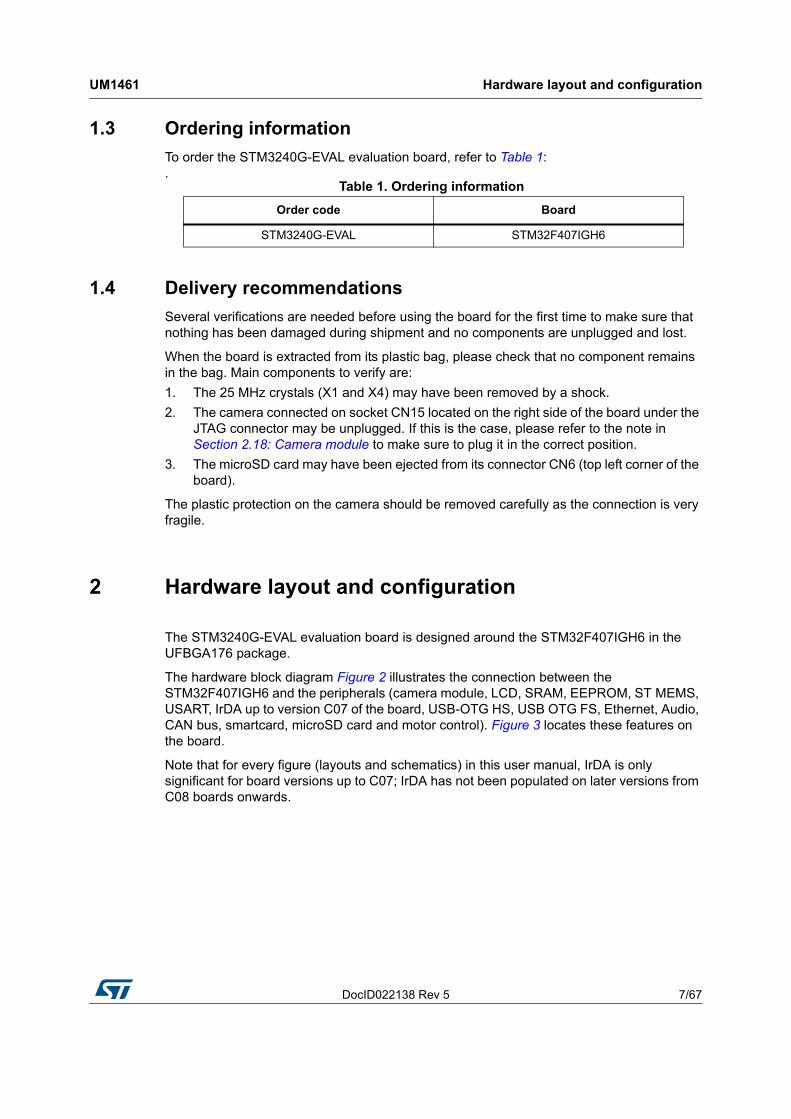
The STM3240G-EVAL evaluation board is designed around the STM32F407IGH6 in the UFBGA176 package.
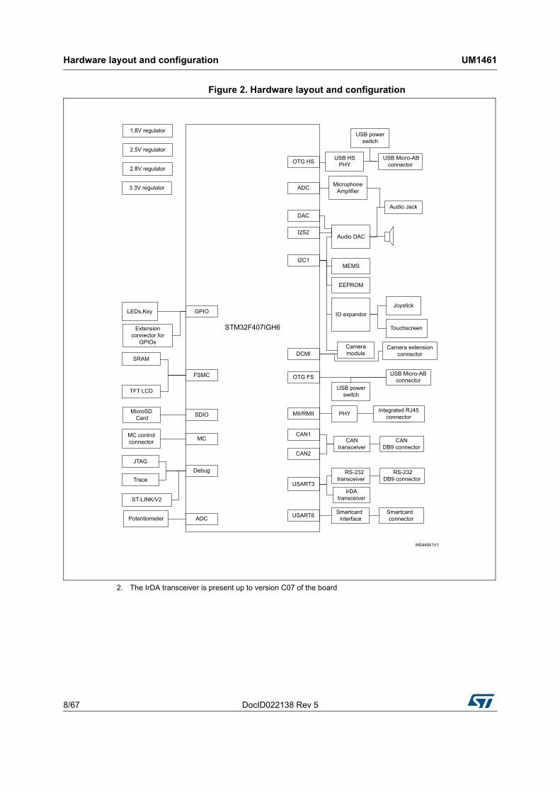
The hardware block diagram Figure 2 illustrates the connection between the STM32F407IGH6 and the peripherals (camera module, LCD, SRAM, EEPROM, ST MEMS, USART, IrDA up to version C07 of the board, USB-OTG HS, USB OTG FS, Ethernet, Audio, CAN bus, smartcard, microSD card and motor control). Figure 3 locates these features on the board.
Note that for every figure (layouts and schematics) in this user manual, IrDA is only significant for board versions up to C07; IrDA has not been populated on later versions from C08 boards onwards.
Table 1. Ordering information
Order code Board
STM3240G-EVAL STM32F407IGH6
Hardware layout and configuration UM1461
8/67 DocID022138 Rev 5
Figure 2. Hardware layout and configuration
2. The IrDA transceiver is present up to version C07 of the board

DocID022138 Rev 5 9/67
UM1461 Hardware layout and configuration
Figure 3. STM3240G-EVAL evaluation board layout
3. IrDA is not populated on the board from version C08 of the board
Hardware layout and configuration UM1461
10/67 DocID022138 Rev 5
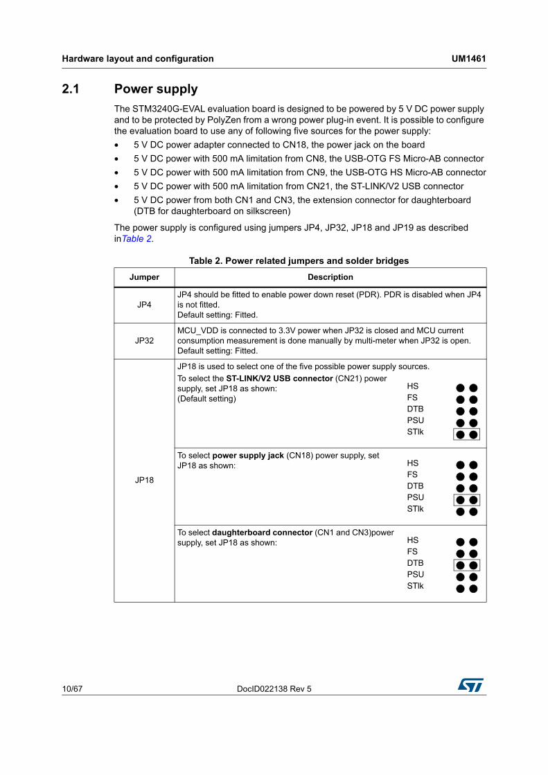
2.1 Power supply
The STM3240G-EVAL evaluation board is designed to be powered by 5 V DC power supply and to be protected by PolyZen from a wrong power plug-in event. It is possible to configure the evaluation board to use any of following five sources for the power supply:
• 5 V DC power adapter connected to CN18, the power jack on the board
• 5 V DC power with 500 mA limitation from CN8, the USB-OTG FS Micro-AB connector
• 5 V DC power with 500 mA limitation from CN9, the USB-OTG HS Micro-AB connector
• 5 V DC power with 500 mA limitation from CN21, the ST-LINK/V2 USB connector
• 5 V DC power from both CN1 and CN3, the extension connector for daughterboard (DTB for daughterboard on silkscreen)
The power supply is configured using jumpers JP4, JP32, JP18 and JP19 as described inTable 2.
Table 2. Power related jumpers and solder bridges
Jumper Description
JP4JP4 should be fitted to enable power down reset (PDR). PDR is disabled when JP4 is not fitted. Default setting: Fitted.
JP32MCU_VDD is connected to 3.3V power when JP32 is closed and MCU current consumption measurement is done manually by multi-meter when JP32 is open. Default setting: Fitted.
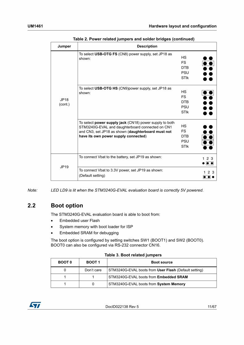
JP18
JP18 is used to select one of the five possible power supply sources.
To select the ST-LINK/V2 USB connector (CN21) power supply, set JP18 as shown: (Default setting)
To select power supply jack (CN18) power supply, set JP18 as shown:
To select daughterboard connector (CN1 and CN3)power supply, set JP18 as shown:
HSFSDTBPSUSTlk
HSFSDTBPSUSTlk
HSFSDTBPSUSTlk
DocID022138 Rev 5 11/67
UM1461 Hardware layout and configuration
Note: LED LD9 is lit when the STM3240G-EVAL evaluation board is correctly 5V powered.
2.2 Boot option
The STM3240G-EVAL evaluation board is able to boot from:
• Embedded user Flash
• System memory with boot loader for ISP
• Embedded SRAM for debugging
The boot option is configured by setting switches SW1 (BOOT1) and SW2 (BOOT0). BOOT0 can also be configured via RS-232 connector CN16.
JP18(cont.)
To select USB-OTG FS (CN8) power supply, set JP18 as shown:
To select USB-OTG HS (CN9)power supply, set JP18 as shown:
To select power supply jack (CN18) power supply to both STM3240G-EVAL and daughterboard connected on CN1 and CN3, set JP18 as shown (daughterboard must not have its own power supply connected)
JP19
To connect Vbat to the battery, set JP19 as shown:
To connect Vbat to 3.3V power, set JP19 as shown:
(Default setting)
Table 2. Power related jumpers and solder bridges (continued)
Jumper Description
HSFSDTBPSUSTlk
HSFSDTBPSUSTlk
HSFSDTBPSUSTlk
321
321
Table 3. Boot related jumpers
BOOT 0 BOOT 1 Boot source
0 Don’t care STM3240G-EVAL boots from User Flash (Default setting)
1 1 STM3240G-EVAL boots from Embedded SRAM
1 0 STM3240G-EVAL boots from System Memory
Hardware layout and configuration UM1461
12/67 DocID022138 Rev 5
2.3 Clock source
Four clock sources are available on the STM3240G-EVAL evaluation board for STM32F407IGH6 and RTC embedded:
• X1, 25 MHz crystal for Ethernet PHY with socket. It can be removed when clock is provided by the MCU MCO pin
• X2, 26 MHz crystal for USB-OTG HS PHY
• X3, 32 kHz crystal for embedded RTC
• X4, 25 MHz crystal with socket for the,STM32F407IGH6 microcontroller (it can be removed from socket when internal RC clock is used)
2.4 Reset source
The reset signal of the STM3240G-EVAL evaluation board is low active and the reset sources include:
• Reset button B1
• Debugging tools from JTAG connector CN14 and trace connector CN13
• Daughterboard from CN3
• RS-232 connector CN916 for ISP
• ST-LINK/V2
2.5 Audio
The STM3240G-EVAL evaluation board enables stereo audio play and microphone recording by an external headset connected on audio jack CN11. An audio DAC CS43L22 is connected to both I2S2 port and a DAC channel and a microphone amplifier is connected to the ADC of the STM32F407IGH6. CS43L22 can be configured via I2C1 and the external PLL (U36) can be used to provide external clock which is connected to I2S_CKIN pin (PC9).
Note: To avoid speaker damage it is mandatory to connect the headphone to the board on CN11 during debug of audio code. When the program is stopped on a breakpoint, a DC voltage may be applied to the speaker which induces power consumption incompatible with the speaker.
Warning: Signal I2S_SD (PI3) is close to signal TCK/SWCLK of the JTAG/SWD interface, so to avoid possible communication issues on JTAG/SWD when the I2S interface is used the recommendations are to: 1) Prefer usage of embedded ST-LINK/V2 to external tool connected on CN14. 2) Configure PI3 GPIO in low speed (2 MHz or 10 MHz).
DocID022138 Rev 5 13/67
UM1461 Hardware layout and configuration
2.6 EEPROM
A 64 Kbit EEPROM is connected to the I2C1 bus of the STM32F407IGH6.
2.7 CAN
The STM3240G-EVAL evaluation board enables two channels of CAN2.0A/B compliant CAN bus communication based on a 3.3V CAN transceiver on one DB9 connector (CN10). The two CAN buses can be disconnected by jumpers from relevant STM32F407IGH6 I/Os which are shared with FSMC and USB-OTG HS. Jumpers JP3 and JP10 must be refit to enable CAN1 or CAN2 as listed in Table 6.
High-speed, Standby and Slope Control modes are available and are selected by setting jumper JP7.
Table 4. Audio related jumpers
Jumper Description
JP16 Description of JP16 is in Table 11 on page 16.
JP33 The microphone amplifier can be disabled when JP33 is fitted.Default setting: Not fitted
Table 5. EEPROM related jumper and solder bridge
Jumper Description
JP24The EEPROM is in Write Protection mode when JP24 is not fitted.
Default Setting: Not fitted
Table 6. CAN-related jumpers
Jumper Description
JP3
To connect CAN1_TX to CAN transceiver, set JP3 as shown:
To connect CAN2_TX to CAN transceiver, set JP3 as shown:
JP10
To connect CAN1_RX to CAN transceiver, set JP10 as shown:
To connect CAN2_RX to CAN transceiver, set JP10 as shown:
PD0 and PB5 are disconnected from the CAN transceiver and used for FSMC and USB_OTG_HS when jumper JP10 is not fitted (default setting).
321
321
321
321
Hardware layout and configuration UM1461
14/67 DocID022138 Rev 5
2.8 RS-232 and IrDA
Both RS-232 and IrDA communication are enabled by D-type, 9-pin RS-232 connectors (CN16) and IrDA transceiver U11 which are connected to USART3 of the STM32F407IGH6 on the STM3240G-EVAL evaluation board.
The IrDA transceiver (TFDU6300) is not populated on STM3240G-EVAL evaluation board from version C08. The version of the board is written on sticker on the bottom side of the board (ex: MB786-C08). For boards version C08 or newer, it is possible to solder manually the TDFU6300 on U11 footprint to support IrDA feature.
For ISP support, two signals are added on the RS-232 connector CN16:
• Bootloader_RESET (shared with CTS signal)
• Bootloader_BOOT0 (shared with DSR signal)
RS-232 or IrDA is selected via JP22. The position 2-3 of jumper JP22 is unused from version C08 of the board. ISP is enabled via JP29 and JP34.
JP7
To enable the selected CAN transceiver to work in Standby mode, set JP7 as shown:
To enable the selected CAN transceiver to work in High-speed mode, set JP7 as shown (default setting):
To enable the selected CAN transceiver to work in Slope Control mode, do not fit a jumper on JP7.
JP9To enable the terminal resistor for the selected CAN, fit a jumper on JP9.
(Default setting: not fitted)
Table 6. CAN-related jumpers (continued)
Jumper Description
321
321
Table 7. RS-232 and IrDA related jumper
Jumper Description
JP22
To connect USART3_RX to IrDA transceiver and enable IrDA communication, set JP22 as shown (this configuration is useless from version C08 of the board):
To connect USART3_RX to RS-232 transceiver and enable RS-232 communication, set JP22 as shown (Default setting):
To enable microSD card, which shares same I/Os with RS-232, JP22 is not fitted.
JP29Bootloader_BOOT0 is managed by pin 6 of CN16 (RS-232 DSR signal) when JP29 is closed. This configuration is used for boot loader application only.
Default setting: Not fitted.
JP34Bootloader_RESET is managed by pin 8 of CN16 (RS-232 CTS signal) when JP34 is fitted. This configuration is used for boot loader application only.
Default setting: Not fitted.
321
321
DocID022138 Rev 5 15/67
UM1461 Hardware layout and configuration
2.9 Motor control
The STM3240G-EVAL evaluation board enables a three-phase brushless motor control via a 34- pin connector (CN5), which provides all required control and feedback signals to and from the motor power-driving board. Available signals on this connector include emergency stop, motor speed, 3-phase motor current, bus voltage, heatsink temperature coming from the motor driving board and 6 channels of PWM control signal going to the motor driving circuit.
The solder bridge (SB18) allows to choose two kinds of synchronization methods for PFCs (Power Factor Correction) while the SB17 can be set for different signals on pin 31 of CN5.
The I/O pins used on motor control connector CN5 are multiplexed with some peripherals on the board; either motor control connector or multiplexed peripherals can be enabled by the setting of solder bridges SB10, SB11, SB12, SB14, SB15 and SB16.
Note: 1 Some 0 Ω resistors have to be removed or soldered to enable motor control application except the solder bridges configurations mentioned above:
– R34, R58 & R51 to be removed
– R66, R204 & R205 to be soldered
2 microSD card must be removed from CN6 for motor control application.
Table 8. Motor control solder bridges
Solder bridge
DescriptionMultiplexed peripherals
SB18
When closed, SB18 redirects the PFC synchronized signal to the timer 3 input capture pin 2 in addition to the timer 3 external trigger input.
Default setting: Open
-
SB17
For CN5 encoder signal input (pin 31), SB17 must be open.
For CN5 special motor analog signal input (pin 31), SB17 must be closed.
Default setting: Open
-
SB16To connect MC_EmergencySTOP to PI4, close SB16.
Default setting: Open
Camera module connected to
CN15
SB10To connect MC_EnIndex to PB8, close SB10.
Default setting: Open
EthernetSB11To connect MC_CurrentA to PC1, close SB11.
Default setting: Open
SB12To connect MC_CurrentB to PC2, close SB12.
Default setting: Open
SB14To connect MC_EnB to PD13, close SB14.
Default setting: OpenFSMC
SB15To connect MC_EnA to PD12 close SB15.
Default setting: Open
Hardware layout and configuration UM1461
16/67 DocID022138 Rev 5
2.10 Smartcard
STMicroelectronics smartcard interface chip ST8024 is used on the STM3240G-EVAL board for asynchronous 3V and 5V smartcards. It performs all supply protection and control functions based on the connections with the STM32F407IGH6 listed in Table 9:
Smartcard shares some I/Os with I2S bus for Audio. Some jumper settings need to be reconfigured to enable smartcard as indicated below:
2.11 microSD card
A 1 Gbyte or more microSD card connected to the STM32F407IGH6 SDIO is available on the board. microSD card detection is managed by the standard I/O port PH13. The microSD card shares I/Os with motor control, RS-232 and audio. The jumpers JP22 and JP16 must be refitted and motor control connector (CN5) must be disconnected for microSD card function.
Table 9. Connection between ST8024 and STM32F407IGH6
ST8024 signals DescriptionConnect to
STM32F407IGH6
5V/3V Smartcard power supply selection pin PH15
I/OUC MCU data I/O line PC6
XTAL1 Crystal or external clock input PG7
OFFDetect presence of a card, MCU interrupt, share same pin with motor controller
PF6
RSTIN Card reset input from MCU PF7
CMDVCCStart activation sequence input (Active Low), share same pin with I2S DAC and Motor control
PG12
Table 10. Smartcard related jumper
Jumper Description
JP21
To connect smartcard_IO to PC6, JP21must be fitted.
JP21 must not be fitted for Audio DAC connection to I2S.
Default setting: Not fitted
Table 11. microSD card related jumpers
Jumper Description
JP22 Description of JP22 is in Section 2.8: RS-232 and IrDA
JP16
PC9 is connected to microSDCard_D1 when JP16 is set as shown to the right: (Default setting):
PC9 is connected to I2S_CKIN when JP16 is set as show to the right:
321
321

DocID022138 Rev 5 17/67
UM1461 Hardware layout and configuration
2.12 ST MEMS
The ST MEMS device LIS302DL is connected to the STM32F407IGH6 I2C1 bus on the board.
2.13 Potentiometer
A 10 kΩ potentiometer RV1 is connected to PF9 of STM32F407IGH6 on the board.
2.14 ADC
Two test points (TP3 AIN-) and (TP4 AIN+) are placed close to port PC1 of the MCU allowing precise measurements on ADC1, ADC2 or ADC3 channel 11. As PC1 is also used as current A input on the motor control connector it is recommended to remove R219 to optimize noise immunity on this input.
A potentiometer RV1 is connected to PF9 of STM32F407IGH6. If needed, a low pass filter (R74 and C59) can be placed on this input to reduce the bandwidth of the analog input PF9.
It is also possible to place the Ethernet PHY (U5) in low power mode in order to reduce the noise induced by this high frequency peripheral. Power down pin (MII_INT in the schematic) is connected to PB14 of the MCU, so this I/O can be configured as output low during analog precision measurement.
2.15 USB-OTG FS
The STM3240G-EVAL evaluation board enables USB-OTG full speed communication via a USB Micro-AB connector (CN8) and USB power switch (U1) connected to VBUS. The evaluation board can be powered by this USB connection at 5V DC with a 500 mA current limitation.
The LED LD6 indicates that the power switch (U1) is ON and STM3240G-EVAL functions as a USB host or that the VBUS is powered by another USB host while STM3240G-EVAL functions as a USB device. The LED LD5 indicates an over-current.
2.16 Ethernet
The STM3240G-EVAL evaluation board enables 10/100M Ethernet communication by a PHY DP83848CVV (U5) and integrated RJ45 connector (CN7). Both MII and RMII interface modes can be selected by setting jumpers JP5, JP6 and JP8 as listed below:
Table 12. Ethernet related jumpers and solder bridges
Jumper Description
JP8
JP8 is used to select MII or RMII interface mode.
To enable MII, JP8 is not fitted. To enable RMII interface mode, JP8 is fitted.
Default setting: Not fitted
Hardware layout and configuration UM1461
18/67 DocID022138 Rev 5
Note: 1 A test point (TP2) is available on the board for the PTP_PPS feature test.
2 The Ethernet PHY (U5) can be powered down by regulating PB14.
3 In RMII mode the 50 MHz clock must be provided to Ethernet PHY by an external oscillator. This oscillator (ref SM7745HEV-50.0M or equivalent) must be soldered on the U3 footprint (located under CN3) and jumper JP5 must be removed. This oscillator is not provided with the board.
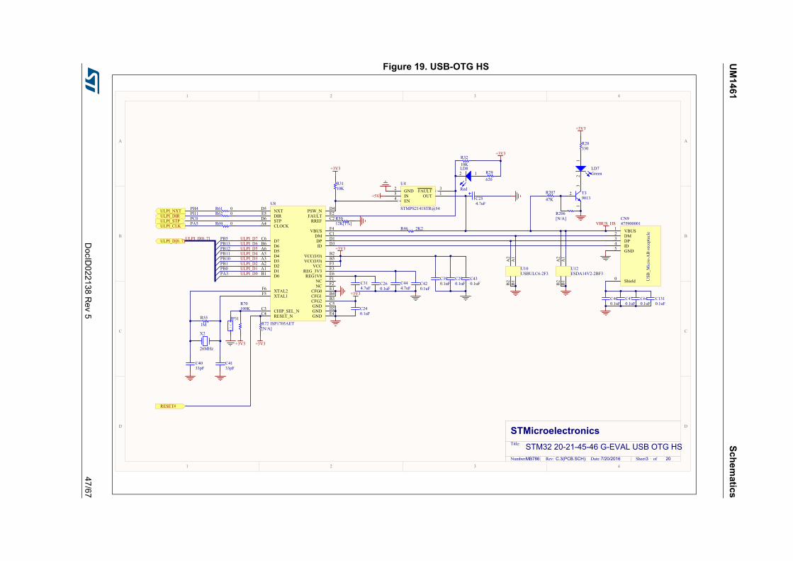
2.17 USB-OTG HS
The STM3240G-EVAL evaluation board enables USB-OTG high speed communication via a USB Micro-AB connector (CN9), USB high speed PHY (U8) and USB power switch (U4) connected to VBUS. The evaluation board can be powered by this USB connector (CN9) at 5V DC with a 500 mA current limitation.
LED LD7 indicates that power switch (U4) is ON and the STM3240G-EVAL is working as a USB host or that VBUS is powered by another USB host when the STM3240G-EVAL is working as a USB device. The LD8 indicates an over-current. The USB ULPI bus is shared with CAN2 bus, the JP10 and JP3 must be kept open for USB-OTG HS.
Note: On boards MB786 prior to version B03 it is possible that after a board RESET the MCU is no longer able to control communication with the OTG PHY (U8). When this issue occurs the only way to recover OTG PHY control is to power the board OFF and ON. This issue is fixed on MB786 version B03 or newer.
JP6
To enable MII interface mode, set JP6 as shown (Default setting):
To enable RMII interface mode, set JP6 as shown:
JP5
To provide 25 MHz clock for MII or 50 MHz clock for RMII by MCO at PA8, set JP5 as shown (Default setting):
To provide 25 MHz clock by external crystal X1 (for MII interface mode only) set JP5 as shown:
When clock is provided by external oscillator U3, JP5 must not be fitted.
SB1
SB1 is used to select clock source only for RMII mode.
To connect the clock from oscillator U3 to RMII_REF_CLK, close SB1.
The resistor R212 has to be removed in this case.
Default setting: Closed.
Table 12. Ethernet related jumpers and solder bridges (continued)
Jumper Description
321
321
321
321
Table 13. microSD card related jumper
Jumper Description
JP31To disable USB-OTG PHY U8, JP31 is not fitted.
Default setting: Fitted
DocID022138 Rev 5 19/67
UM1461 Hardware layout and configuration
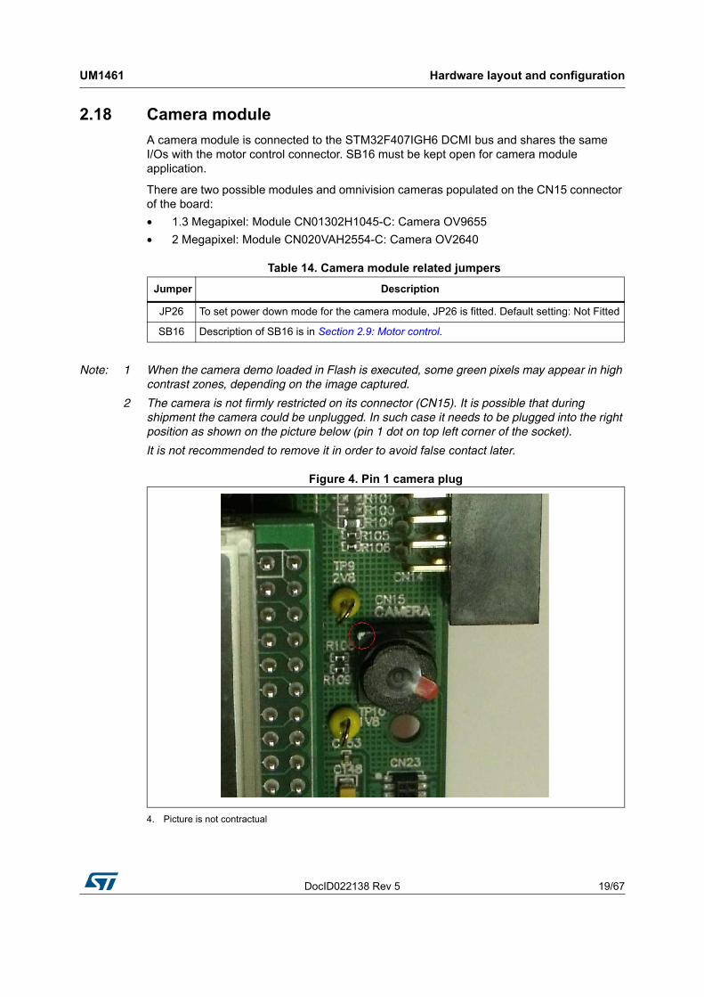
2.18 Camera module
A camera module is connected to the STM32F407IGH6 DCMI bus and shares the same I/Os with the motor control connector. SB16 must be kept open for camera module application.
There are two possible modules and omnivision cameras populated on the CN15 connector of the board:
• 1.3 Megapixel: Module CN01302H1045-C: Camera OV9655
• 2 Megapixel: Module CN020VAH2554-C: Camera OV2640
Note: 1 When the camera demo loaded in Flash is executed, some green pixels may appear in high contrast zones, depending on the image captured.
2 The camera is not firmly restricted on its connector (CN15). It is possible that during shipment the camera could be unplugged. In such case it needs to be plugged into the right position as shown on the picture below (pin 1 dot on top left corner of the socket).
It is not recommended to remove it in order to avoid false contact later.
Figure 4. Pin 1 camera plug
4. Picture is not contractual
Table 14. Camera module related jumpers
Jumper Description
JP26 To set power down mode for the camera module, JP26 is fitted. Default setting: Not Fitted
SB16 Description of SB16 is in Section 2.9: Motor control.
Hardware layout and configuration UM1461
20/67 DocID022138 Rev 5
The camera extension connector CN23 is available on the boards to connect the ST camera plug-in board.
2.19 SRAM
The 16 Mbit SRAM is connected to the STM32F407IGH6 FSMC bus which shares the same I/Os with the CAN1 bus. JP3 and JP10 must not be fitted for SRAM and LCD application.
2.20 Development and debug support
Version 2 of the ST-LINK, called ST-LINK/V2, is embedded on the board. This tool allows onboard program loading and debugging of the STM32F using the JTAG or SWD interface. Third-party debug tools are also supported by the JTAG (CN14) or Trace (CN13) connectors.
Note: Due to I/O sharing on the board there is a frequency limitation on ETM trace, so when the MCU clock is above 120 MHz the ETM trace output is not guaranteed.
To communicate with the embedded ST-LINK/V2, a specific driver needs to be installed on your PC. To download and install this driver, refer to the software and development tools page for the STM32F family available on www.st.com (the install shield is called ST-LINK_V2_USBdriver.exe).
Third-party toolchains, Atollic TrueSTUDIO, KEIL ARM-MDK, IAR EWARM and Tasking VX-Toolset support ST-LINK/V2 according to the following table:
The embedded ST-LINK/V2 connects to the PC via a standard USB cable from connector CN21.
Table 15. SRAM related jumpers
Jumper Description
JP1
Connect PE4 to SRAM as A20 by setting JP1 as shown (Default setting):
Connect PE4 to trace connector CN13 as TRACE_D1 by setting JP1 as shown:
JP2
Connect PE3 to SRAM as A19 by settiing JP2 as shown (Default setting):
Connect PE3 to trace connector CN13 as TRACE_D0 by setting JP2 as shown:
321
321
321
321
Table 16. Third-party toolchain support
Manufacturer Toolchain Version
Atollic TrueSTUDIO 2.1
IAR EWARM 6.20.4
Keil MDK-ARM 4.20
Tasking VX-Toolset ARM Cortex-M 4.0.1
DocID022138 Rev 5 21/67
UM1461 Hardware layout and configuration
The bicolor LED LD10 (COM) indicates the status of the communication as follows:
• Slow blinking Red/Off: At power-on before USB initialization
• Fast blinking Red/Off: After the first correct communication between PC and ST-LINK/V2 (enumeration)
• Red LED On: When initialization between PC and ST-LINK/V2 is successfully finished
• Green LED On: After successful target communication initialization
• Blinking Red/Green: During communication with target
• Green On: Communication finished and OK
• Orange On: Communication failure
Note: 1 It is possible to power the board via CN21 (embedded ST-LINK/V2 USB connector) even if an external tool is connected to CN13 (trace) or CN14 (external JTAG and SWD).
2 If the I2S interface is used, refer to the warning in Chapter 2.5.
Hardware layout and configuration UM1461
22/67 DocID022138 Rev 5
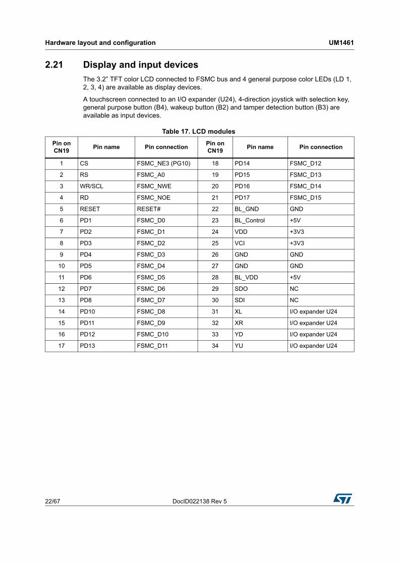
2.21 Display and input devices
The 3.2” TFT color LCD connected to FSMC bus and 4 general purpose color LEDs (LD 1, 2, 3, 4) are available as display devices.
A touchscreen connected to an I/O expander (U24), 4-direction joystick with selection key, general purpose button (B4), wakeup button (B2) and tamper detection button (B3) are available as input devices.
Table 17. LCD modules
Pin on CN19
Pin name Pin connectionPin on CN19
Pin name Pin connection
1 CS FSMC_NE3 (PG10) 18 PD14 FSMC_D12
2 RS FSMC_A0 19 PD15 FSMC_D13
3 WR/SCL FSMC_NWE 20 PD16 FSMC_D14
4 RD FSMC_NOE 21 PD17 FSMC_D15
5 RESET RESET# 22 BL_GND GND
6 PD1 FSMC_D0 23 BL_Control +5V
7 PD2 FSMC_D1 24 VDD +3V3
8 PD3 FSMC_D2 25 VCI +3V3
9 PD4 FSMC_D3 26 GND GND
10 PD5 FSMC_D4 27 GND GND
11 PD6 FSMC_D5 28 BL_VDD +5V
12 PD7 FSMC_D6 29 SDO NC
13 PD8 FSMC_D7 30 SDI NC
14 PD10 FSMC_D8 31 XL I/O expander U24
15 PD11 FSMC_D9 32 XR I/O expander U24
16 PD12 FSMC_D10 33 YD I/O expander U24
17 PD13 FSMC_D11 34 YU I/O expander U24
DocID022138 Rev 5 23/67
UM1461 Connectors
3 Connectors
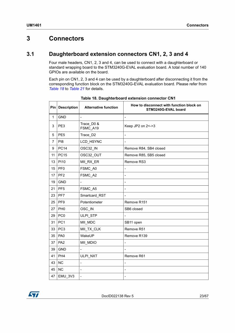
3.1 Daughterboard extension connectors CN1, 2, 3 and 4
Four male headers, CN1, 2, 3 and 4, can be used to connect with a daughterboard or standard wrapping board to the STM3240G-EVAL evaluation board. A total number of 140 GPIOs are available on the board.
Each pin on CN1, 2, 3 and 4 can be used by a daughterboard after disconnecting it from the corresponding function block on the STM3240G-EVAL evaluation board. Please refer from Table 18 to Table 21 for details.
Table 18. Daughterboard extension connector CN1
Pin Description Alternative functionHow to disconnect with function block on
STM3240G-EVAL board
1 GND - -
3 PE3Trace_D0 & FSMC_A19
Keep JP2 on 2<->3
5 PE5 Trace_D2 -
7 PI8 LCD_HSYNC -
9 PC14 OSC32_IN Remove R84, SB4 closed
11 PC15 OSC32_OUT Remove R85, SB5 closed
13 PI10 MII_RX_ER Remove RS3
15 PF0 FSMC_A0 -
17 PF2 FSMC_A2 -
19 GND - -
21 PF5 FSMC_A5 -
23 PF7 Smartcard_RST -
25 PF9 Potentiometer Remove R151
27 PH0 OSC_IN SB6 closed
29 PC0 ULPI_STP -
31 PC1 MII_MDC SB11 open
33 PC3 MII_TX_CLK Remove R51
35 PA0 WakeUP Remove R139
37 PA2 MII_MDIO -
39 GND - -
41 PH4 ULPI_NXT Remove R61
43 NC - -
45 NC - -
47 EMU_3V3 - -

Connectors UM1461
24/67 DocID022138 Rev 5
49 EMU_5V - -
2 PE2 Trace_CLK -
4 PE4Trace_D1 & FSMC_A20
Keep JP1 on 2<->3
6 PE6 Trace_D3 -
8 PC13 Anti-Tamper Remove R143
10 GND - -
12 PI9 LED3 Remove R141
14 PI11 ULPI_DIR Remove R62
16 PF1 FSMC_A1 -
18 PF3 FSMC_A3 -
20 PF4 FSMC_A4 -
22 PF6 Smartcard_OFF Remove R126
24 PF8 LCD_CS -
26 PF10 Audio_IN Remove R196
28 PH1 OSC_OUT Remove R86, SB7 closed
30 GND - -
32 PC2MII_TXD2 & MC
SB12 open
34 VREF+ - -
36 PA1 MII_RX_CLK JP6 open
38 PH2 MII_CRS Remove RS3
40 PH3 MII_COL Remove RS3
42 PH5 OTG_FS_PowerSwitchOn Remove R18
44 NC - -
46 NC - -
48 APP_3V3 - -
50 GND - -
Table 18. Daughterboard extension connector CN1 (continued)
Pin Description Alternative functionHow to disconnect with function block on
STM3240G-EVAL board
DocID022138 Rev 5 25/67
UM1461 Connectors
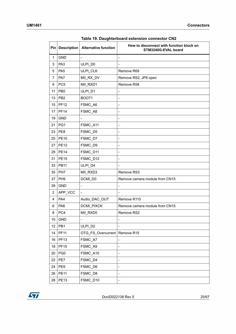
Table 19. Daughterboard extension connector CN2
Pin Description Alternative functionHow to disconnect with function block on
STM3240G-EVAL board
1 GND - -
3 PA3 ULPI_D0 -
5 PA5 ULPI_CLK Remove R69
7 PA7 MII_RX_DV Remove RS2, JP8 open
9 PC5 MII_RXD1 Remove R58
11 PB0 ULPI_D1 -
13 PB2 BOOT1 -
15 PF12 FSMC_A6 -
17 PF14 FSMC_A8 -
19 GND - -
21 PG1 FSMC_A11 -
23 PE8 FSMC_D5 -
25 PE10 FSMC_D7 -
27 PE12 FSMC_D9 -
29 PE14 FSMC_D11 -
31 PE15 FSMC_D12 -
33 PB11 ULPI_D4 -
35 PH7 MII_RXD3 Remove RS3
37 PH9 DCMI_D0 Remove camera module from CN15
39 GND - -
2 APP_VCC - -
4 PA4 Audio_DAC_OUT Remove R115
6 PA6 DCMI_PIXCK Remove camera module from CN15
8 PC4 MII_RXD0 Remove RS2
10 GND - -
12 PB1 ULPI_D2 -
14 PF11 OTG_FS_Overcurrent Remove R15
16 PF13 FSMC_A7 -
18 PF15 FSMC_A9 -
20 PG0 FSMC_A10 -
22 PE7 FSMC_D4 -
24 PE9 FSMC_D6 -
26 PE11 FSMC_D8 -
28 PE13 FSMC_D10 -
Connectors UM1461
26/67 DocID022138 Rev 5
30 GND - -
32 PB10 ULPI_D3 -
34 PH6 MII_RXD2 Remove RS5
36 PH8DCMI_HSYNC & MC
Remove camera module from CN15. Disconnect motor control board from CN5.
38 PH10DCMI_D1 & MC
Remove camera module from CN15. Disconnect motor control board from CN5.
40 PH11DCMI_D2 & MC
Remove camera module from CN15. Disconnect motor control board from CN5.
Table 20. Daughterboard extension connector CN3
Pin Description Alternative functionHow to disconnect with function block on
STM3240G-EVAL board
1 GND - -
3 PI1 I2S_CK -
5 PH15Smartcard_3/5V & MC
Disconnect motor control board from CN5
7 PH13MicroSDCard_detect & MC
Remove microSD card from CN6. Disconnect motor control board from CN5.
9 PC13 Anti-tamper Remove R143
11 RESET# Reset button -
13 PA11 OTG_FS_DM Remove R17
15 PA9 VBUS_FSRemove USB cable from CN8.
Remove R18.
17 PC9MicroSDCard_D1 & I2S_CKIN
Keep JP16 on open
19 EMU_5V - -
21 PC6I2S_MCK & Smartcard_IO
JP21 open
23 PG7 Smartcard_CLK -
25 PG5 FSMC_A15 -
27 PG3 FSMC_A13 -
29 PD15 FSMC_D1 -
31 PD14 FSMC_D0 -
33 PD12 FSMC_A17 SB15 open
35 PD10 FSMC_D15 -
37 PD8 FSMC_D13 -
Table 19. Daughterboard extension connector CN2 (continued)
Pin Description Alternative functionHow to disconnect with function block on
STM3240G-EVAL board

DocID022138 Rev 5 27/67
UM1461 Connectors
39 GND - -
41 PB13ULPI_D6 & CAN2_TX
-
43 PH12DCMI_D3 & MC
Remove camera module from CN15.
Disconnect motor control board from CN5.
45 NC - -
47 EMU_3V3 - -
49 EMU_5V - -
2 PI2 IO_Expandor_INT Remove R136
4 PI0 I2S_CMD -
6 PH14DCMI_D4 & MC
Remove camera module from CN15.
Disconnect motor control board from CN5.
8 PA13 TMS/SWDIO -
10 GND - -
12 PA12 OTG_FS_DP Remove R19
14 PA10 OTG_FS_ID Remove R21
16 PA8 MCO JP5 open
18 PC8MicroSDCard_D0 & MC
Remove microSD card from CN6.
Disconnect motor control board from CN5.
20 PC7 LED4 Remove R140
22 PG8 LED2 Remove R154
24 PG6 LED1 Remove R155
26 PG4 FSMC_A14 -
28 PG2 FSMC_A12 -
30 GND - -
32 PD13 FSMC/MCSB14 open.
Disconnect motor control board from CN5.
34 PD11 FSMC_A16 -
36 PD9 FSMC_D14 -
38 PB15 OneNAND_INT Remove R53
40 PB14 MII_INT Remove R41
42 PB12 ULPI_D5 -
44 NC - -
46 NC - -
Table 20. Daughterboard extension connector CN3 (continued)
Pin Description Alternative functionHow to disconnect with function block on
STM3240G-EVAL board
Connectors UM1461
28/67 DocID022138 Rev 5
48 APP_3V3 - -
50 GND - -
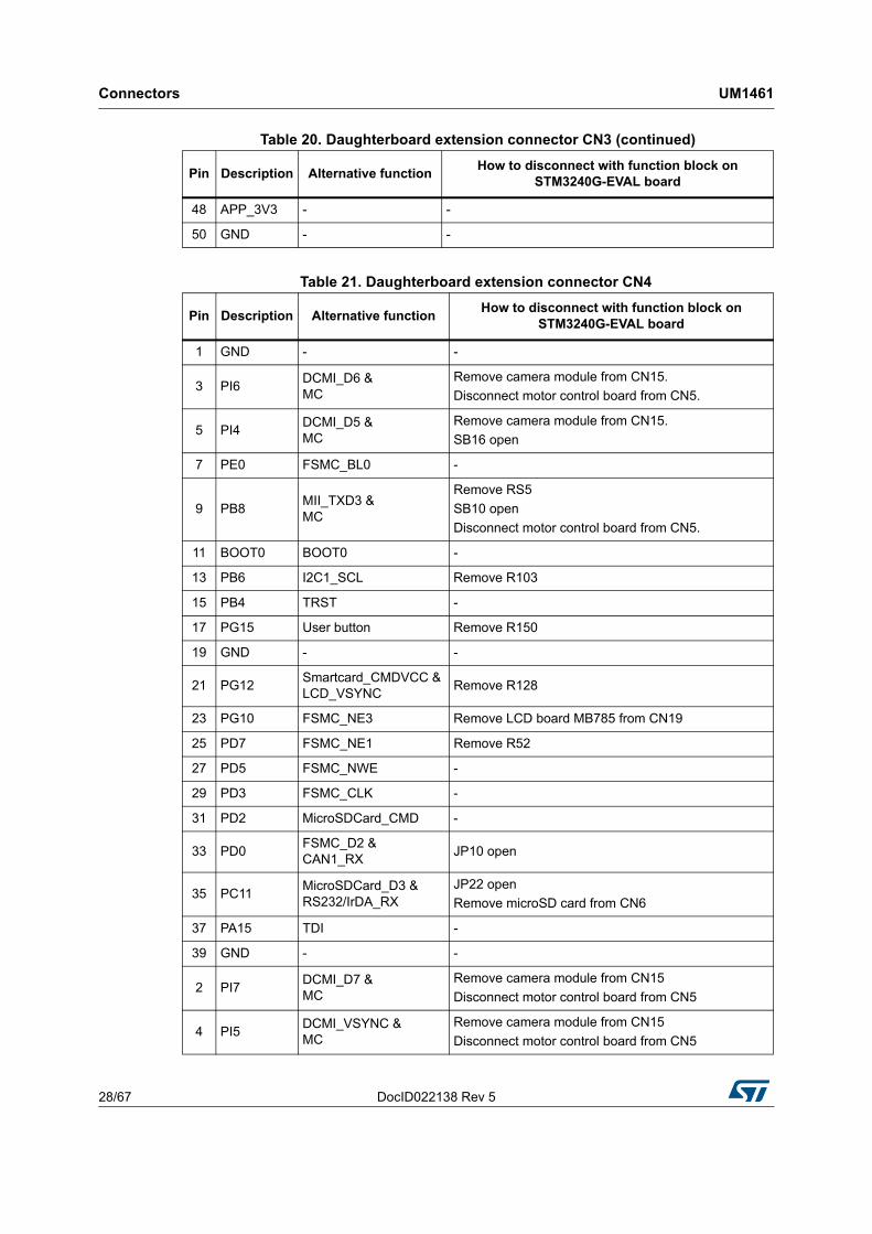
Table 21. Daughterboard extension connector CN4
Pin Description Alternative functionHow to disconnect with function block on
STM3240G-EVAL board
1 GND - -
3 PI6DCMI_D6 & MC
Remove camera module from CN15.
Disconnect motor control board from CN5.
5 PI4DCMI_D5 & MC
Remove camera module from CN15.
SB16 open
7 PE0 FSMC_BL0 -
9 PB8MII_TXD3 & MC
Remove RS5
SB10 open
Disconnect motor control board from CN5.
11 BOOT0 BOOT0 -
13 PB6 I2C1_SCL Remove R103
15 PB4 TRST -
17 PG15 User button Remove R150
19 GND - -
21 PG12Smartcard_CMDVCC & LCD_VSYNC
Remove R128
23 PG10 FSMC_NE3 Remove LCD board MB785 from CN19
25 PD7 FSMC_NE1 Remove R52
27 PD5 FSMC_NWE -
29 PD3 FSMC_CLK -
31 PD2 MicroSDCard_CMD -
33 PD0FSMC_D2 & CAN1_RX
JP10 open
35 PC11MicroSDCard_D3 & RS232/IrDA_RX
JP22 open
Remove microSD card from CN6
37 PA15 TDI -
39 GND - -
2 PI7DCMI_D7 & MC
Remove camera module from CN15
Disconnect motor control board from CN5
4 PI5DCMI_VSYNC & MC
Remove camera module from CN15
Disconnect motor control board from CN5
Table 20. Daughterboard extension connector CN3 (continued)
Pin Description Alternative functionHow to disconnect with function block on
STM3240G-EVAL board

DocID022138 Rev 5 29/67
UM1461 Connectors
6 PE1 FSMC_BL1 -
8 PB9 I2C1_SDA Remove R111
10 GND - -
12 PB7 FSMC_NL -
14 PB5ULPI_D7 & CAN2_RX
JP10 open
16 PB3 TDO/SWO -
18 PG14 MII_TXD1 Remove RS6
20 PG13 MII_TXD0 Remove RS6
22 PG11 MII_TX_EN Remove RS6
24 PG9 FSMC_NE2 Remove R47
26 PD6 FSMC_NWAIT Remove R54
28 PD4 FSMC_NOE -
30 GND - -
32 PD1FSMC_D3 & CAN1_TX
JP3 open
34 PC12 MicroSDCard_CLK Remove microSD card from CN6
36 PC10MicroSDCard_D2 & RS232/IrDA_TX
Remove microSD card from CN6
38 PA14 TCK/SWCLK -
40 PI3 I2S_DIN -
Table 21. Daughterboard extension connector CN4 (continued)
Pin Description Alternative functionHow to disconnect with function block on
STM3240G-EVAL board
Connectors UM1461
30/67 DocID022138 Rev 5
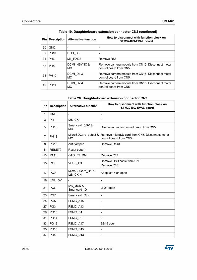
3.2 Motor control connector CN5
Figure 5. Motor control connector CN5
Table 22. Motor control connector CN5
Description STM32F407IGH6
pinCN5 pin CN5 pin
STM32F407IGH6 pin Description
EMERGENCY STOP
PI4 1 2 - GND
PWM-UH PI5 3 4 - GND
PWM-UL PH13 5 6 - GND
PWM-VH PI6 7 8 - GND
PWM-VL PH14 9 10 - GND
PWM-WH PI7 11 12 - GND
PWM-WL PH15 13 14 PC4BUS
VOLTAGE
PHASE A CURRENT
PC1 15 16 - GND
PHASE B CURRENT
PC2 17 18 - GND
PHASE C CURRENT
PC3 19 20 - GND
NTC BYPASS RELAY
PH8 21 22 - GND
DISSIPATIVE BRAKE PWM
PC8 23 24 - GND
+5V power +5V 25 26 PC5Heatsink
temperature
PFC SYNC PH10 and PH11 27 28 - VDD_Micro
PFC PWM PH12 29 30 - GND
Encoder A PD12 31 32 - GND
Encoder B PD13 33 34 PB8Encoder
Index

DocID022138 Rev 5 31/67
UM1461 Connectors
3.3 microSD connector CN6
Figure 6. microSD connector CN6
m
3.4 Ethernet RJ45 connector CN7
Figure 7. Ethernet RJ45 connector CN7
Table 23. microSD connector CN6
Pin Description Pin Description
1 SDIO_D2 (PC10) 5 SDIO_CLK (PC12)
2 SDIO_D3 (PC11) 6 Vss/GND
3 SDIO_CMD (PD2) 7 SDIO_D0 (PC8)
4 +3V3 8 SDIO_D1 (PC9)
- 10 MicroSDcard_detect (PH13)
Table 24. RJ45 connector CN7
Pin Description Pin Description
1 TxData+ 2 TxData-
3 RxData+ 4 Shield
5 Shield 6 RxData-
7 Shield 8 Shield
Connectors UM1461
32/67 DocID022138 Rev 5
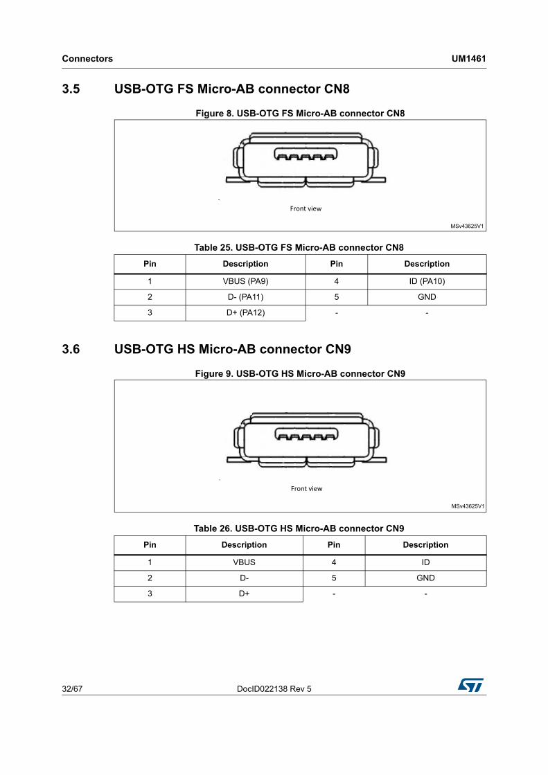
3.5 USB-OTG FS Micro-AB connector CN8
Figure 8. USB-OTG FS Micro-AB connector CN8
3.6 USB-OTG HS Micro-AB connector CN9
Figure 9. USB-OTG HS Micro-AB connector CN9
Table 25. USB-OTG FS Micro-AB connector CN8
Pin Description Pin Description
1 VBUS (PA9) 4 ID (PA10)
2 D- (PA11) 5 GND
3 D+ (PA12) - -
Table 26. USB-OTG HS Micro-AB connector CN9
Pin Description Pin Description
1 VBUS 4 ID
2 D- 5 GND
3 D+ - -
DocID022138 Rev 5 33/67
UM1461 Connectors
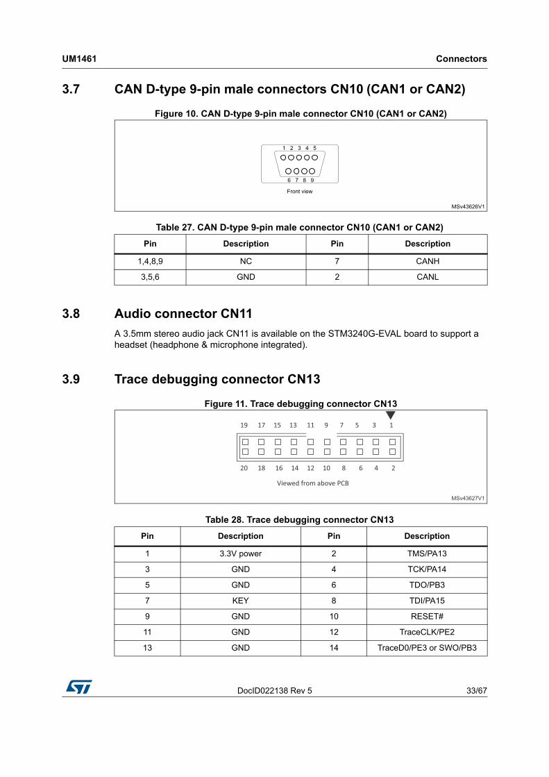
3.7 CAN D-type 9-pin male connectors CN10 (CAN1 or CAN2)
Figure 10. CAN D-type 9-pin male connector CN10 (CAN1 or CAN2)
3.8 Audio connector CN11
A 3.5mm stereo audio jack CN11 is available on the STM3240G-EVAL board to support a headset (headphone & microphone integrated).
3.9 Trace debugging connector CN13
Figure 11. Trace debugging connector CN13
Table 27. CAN D-type 9-pin male connector CN10 (CAN1 or CAN2)
Pin Description Pin Description
1,4,8,9 NC 7 CANH
3,5,6 GND 2 CANL
Table 28. Trace debugging connector CN13
Pin Description Pin Description
1 3.3V power 2 TMS/PA13
3 GND 4 TCK/PA14
5 GND 6 TDO/PB3
7 KEY 8 TDI/PA15
9 GND 10 RESET#
11 GND 12 TraceCLK/PE2
13 GND 14 TraceD0/PE3 or SWO/PB3
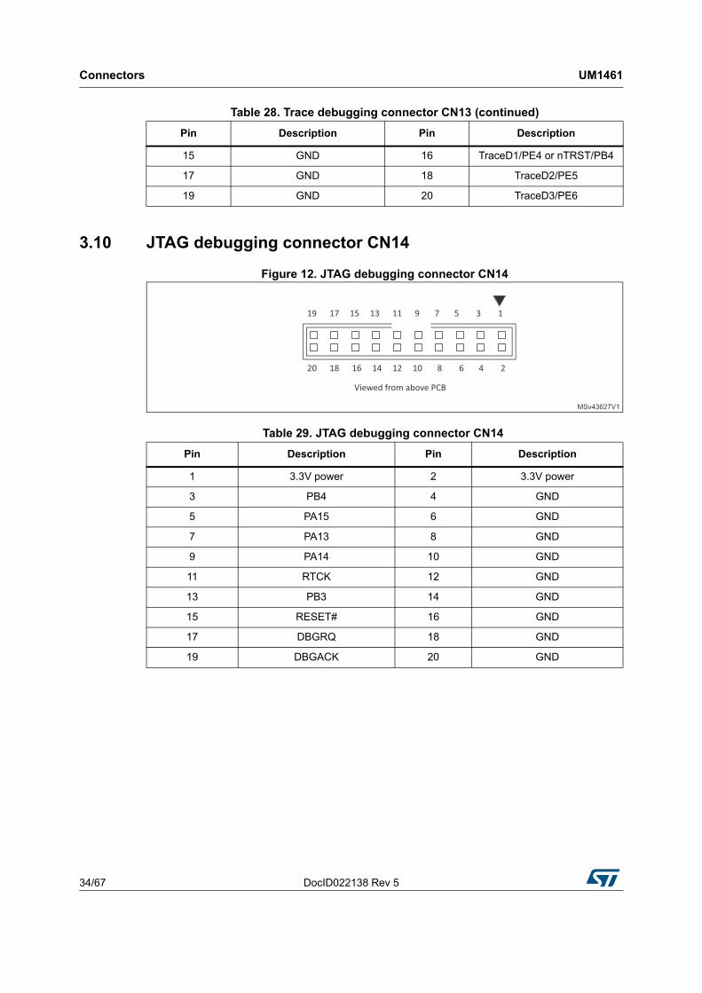
Connectors UM1461
34/67 DocID022138 Rev 5
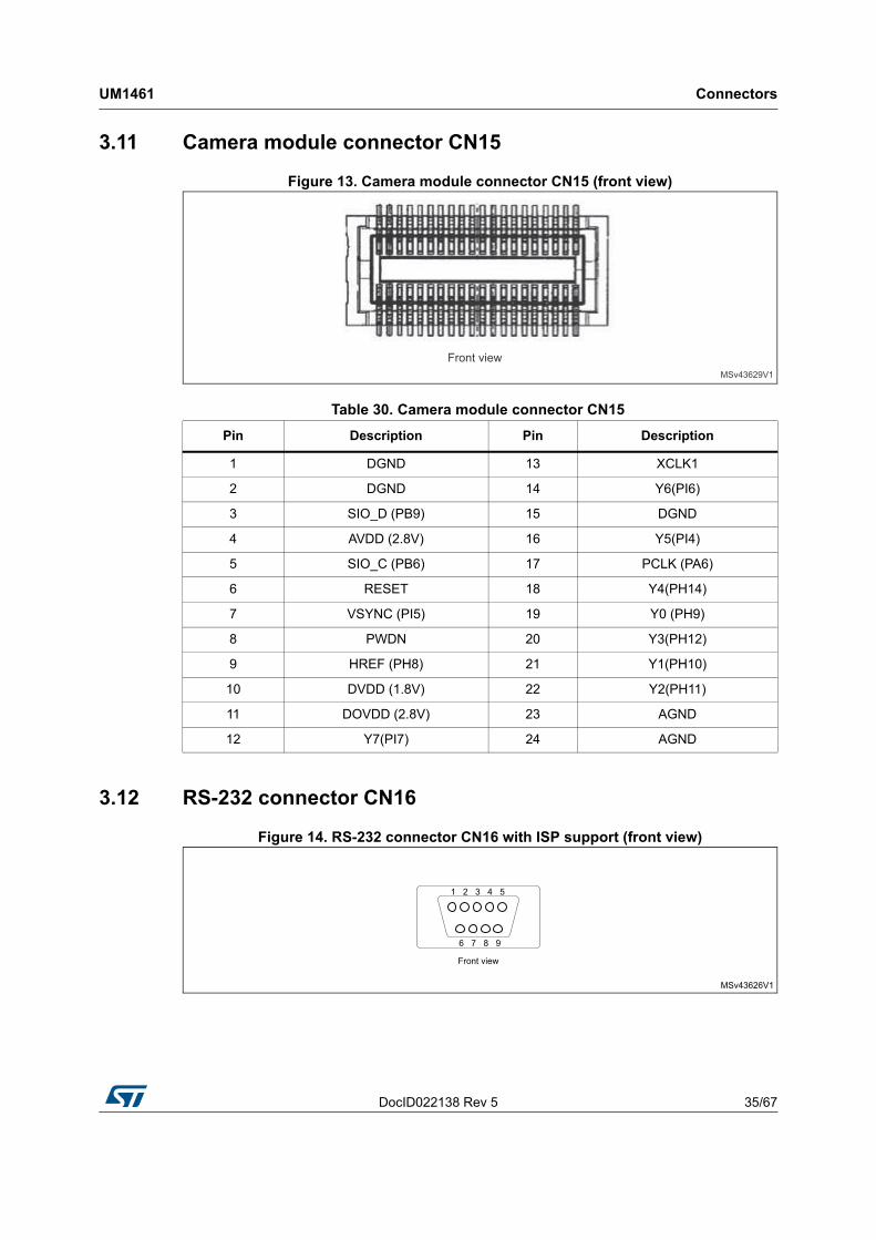
3.10 JTAG debugging connector CN14
Figure 12. JTAG debugging connector CN14
15 GND 16 TraceD1/PE4 or nTRST/PB4
17 GND 18 TraceD2/PE5
19 GND 20 TraceD3/PE6
Table 28. Trace debugging connector CN13 (continued)
Pin Description Pin Description
Table 29. JTAG debugging connector CN14
Pin Description Pin Description
1 3.3V power 2 3.3V power
3 PB4 4 GND
5 PA15 6 GND
7 PA13 8 GND
9 PA14 10 GND
11 RTCK 12 GND
13 PB3 14 GND
15 RESET# 16 GND
17 DBGRQ 18 GND
19 DBGACK 20 GND
DocID022138 Rev 5 35/67
UM1461 Connectors
3.11 Camera module connector CN15
Figure 13. Camera module connector CN15 (front view)
3.12 RS-232 connector CN16
Figure 14. RS-232 connector CN16 with ISP support (front view)
Table 30. Camera module connector CN15
Pin Description Pin Description
1 DGND 13 XCLK1
2 DGND 14 Y6(PI6)
3 SIO_D (PB9) 15 DGND
4 AVDD (2.8V) 16 Y5(PI4)
5 SIO_C (PB6) 17 PCLK (PA6)
6 RESET 18 Y4(PH14)
7 VSYNC (PI5) 19 Y0 (PH9)
8 PWDN 20 Y3(PH12)
9 HREF (PH8) 21 Y1(PH10)
10 DVDD (1.8V) 22 Y2(PH11)
11 DOVDD (2.8V) 23 AGND
12 Y7(PI7) 24 AGND

Connectors UM1461
36/67 DocID022138 Rev 5
3.13 Power connector CN18
The STM3240G-EVAL evaluation board can be powered by a 5 V DC power supply via the external power supply jack (CN18) shown in Figure 15. CN18 central pin must be positive.
Figure 15. Power supply connector CN18
3.14 TFT LCD connector CN19
One 34-pin male header CN19 is available on the board for connecting LCD module board MB785.
Please refer to Section 2.21: Display and input devices for details.
3.15 Smartcard connector CN20
Figure 16. Smartcard connector CN20
Table 31. RS-232 connector CN16 with ISP support
Pin Description Pin Description
1 NC 6 Bootloader_BOOT0
2 RS232_RX (PC11) 7 NC
3 RS232_TX (PC10) 8 Bootloader_RESET
4 NC 9 NC
5 GND -

DocID022138 Rev 5 37/67
UM1461 Connectors
3.16 ST-LINK/V2 connector CN21
The USB type B connector CN21 is intended for ST-LINK/V2 to connect between the STM3240G-EVAL evaluation board and the PC for board debugging.
Table 32. Smartcard connector CN20
Pin Description Pin Description
1 VCC 5 GND
2 RST 6 NC
3 CLK 7 I/O
4 NC 8 NC
17 Card presence detection pin 18 Card presence detection pin

Connectors UM1461
38/67 DocID022138 Rev 5
3.17 Camera extension connector CN23
3.18 STM3240G-EVAL pinout
Table 33. Camera extension connector CN23
Pin Description Pin Description
1 +1V8 2 +1V8
3 GND 4 GND
5 NC 6 NC
7 GND 8 GND
9 NC 10 NC
11 GND 12 GND
13 SCL 14 SDA
15 Camera_Plug 16 GND
17 Camera_RST 18 NC
19 Camera_XSDN 20 Camera_CLK
21 GND 22 GND
23 DCMI_D0 24 DCMI_D1
25 DCMI_D2 26 DCMI_D3
27 DCMI_D4 28 DCMI_D5
29 DCMI_D6 30 DCMI_D7
31 HSYSC 32 VSYSC
33 PIXCLK 34 NC
35 NC 36 NC
37 GND 38 GND
39 +2V8 40 +2V8
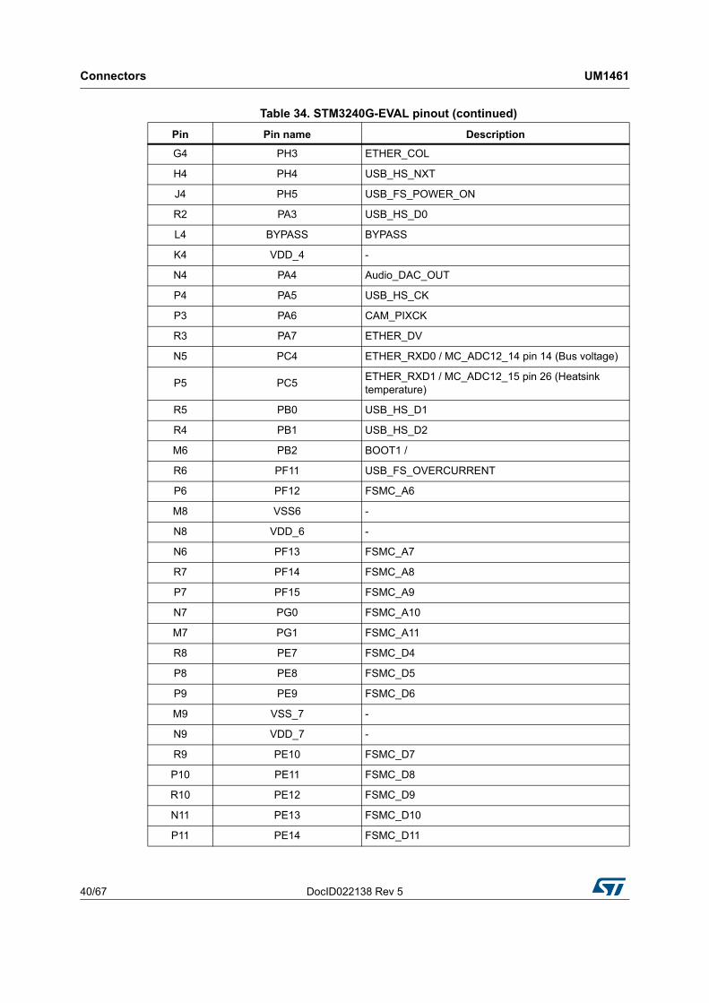
Table 34. STM3240G-EVAL pinout
Pin Pin name Description
A2 PE2 TRACE_CLK / FSMC_A23
A1 PE3 TRACE_D0 / FSMC_A19
B1 PE4 TRACE_D1 / FSMC_A20
B2 PE5 TRACE_D2 / FSMC_A21
B3 PE6 TRACE_D3 / FSMC_A22
C1 VBAT VBAT
D2 PI8- ANTI TAMP2 LCD_HSYNC
D1 PC13-ANTI_TAMP ANTI-TAMPER_BUTTON
DocID022138 Rev 5 39/67
UM1461 Connectors
E1 PC14-OSC32_IN 32K_OSC
F1 PC15-OSC32_OUT 32K_OSC
D3 PI9 LED2
E3 PI10 ETHER_RX_ER
E4 PI11 USB_HS_DIR
F2 VSS_13 -
F3 VDD_13 -
E2 PF0 FSMC_A0
H3 PF1 FSMC_A1
H2 PF2 FSMC_A2
J2 PF3 FSMC_A3
J3 PF4 FSMC_A4
K3 PF5 FSMC_A5
G2 VSS_5 -
G3 VDD_5 -
K2 PF6 SmartCard_OFF
K1 PF7 SmartCard_RESET
L3 PF8 LCD_CS
L2 PF9 POTENTIOMETER
L1 PF10 Audio_IN
G1 PH0 - OSC_IN OSC_IN
H1 PH1 - OSC_OUT OSC_OUT
J1 NRST RESET_BUTTON
M2 PC0 USB_HS_STP
M3 PC1 ETHER_MDC / MC_ADC123_11 pin 15 (Current A)
M4 PC2 ETHER_TXD2 / MC_ADC123_1 2 pin 17 (Current B)
M5 PC3 ETHER_TX_CLK / MC_ADC123_13 pin 19 (Current C)
M1 VSSA -
N1 VREF- -
P1 VREF+ -
R1 VDDA -
N3 PA0-WKUP WAKEUP_BUTTON
N2 PA1 ETHER_RX_CLK
P2 PA2 ETHER_MDIO
F4 PH2 ETHER_CRS
Table 34. STM3240G-EVAL pinout (continued)
Pin Pin name Description
Connectors UM1461
40/67 DocID022138 Rev 5
G4 PH3 ETHER_COL
H4 PH4 USB_HS_NXT
J4 PH5 USB_FS_POWER_ON
R2 PA3 USB_HS_D0
L4 BYPASS BYPASS
K4 VDD_4 -
N4 PA4 Audio_DAC_OUT
P4 PA5 USB_HS_CK
P3 PA6 CAM_PIXCK
R3 PA7 ETHER_DV
N5 PC4 ETHER_RXD0 / MC_ADC12_14 pin 14 (Bus voltage)
P5 PC5ETHER_RXD1 / MC_ADC12_15 pin 26 (Heatsink temperature)
R5 PB0 USB_HS_D1
R4 PB1 USB_HS_D2
M6 PB2 BOOT1 /
R6 PF11 USB_FS_OVERCURRENT
P6 PF12 FSMC_A6
M8 VSS6 -
N8 VDD_6 -
N6 PF13 FSMC_A7
R7 PF14 FSMC_A8
P7 PF15 FSMC_A9
N7 PG0 FSMC_A10
M7 PG1 FSMC_A11
R8 PE7 FSMC_D4
P8 PE8 FSMC_D5
P9 PE9 FSMC_D6
M9 VSS_7 -
N9 VDD_7 -
R9 PE10 FSMC_D7
P10 PE11 FSMC_D8
R10 PE12 FSMC_D9
N11 PE13 FSMC_D10
P11 PE14 FSMC_D11
Table 34. STM3240G-EVAL pinout (continued)
Pin Pin name Description

DocID022138 Rev 5 41/67
UM1461 Connectors
R11 PE15 FSMC_D12
R12 PB10 USB_HS_D3
R13 PB11 ULPI_D4
M10 VCAP1 VCAP / 1.2V
N10 VDD_1 -
M11 PH6 ETHER_RXD2
N12 PH7 ETHER_RXD3
M12 PH8 CAM_HSYNC / MC_NTC_bypass
M13 PH9 CAM_D0
L13 PH10 CAM_D1 / MC_TIM5_ETR pin 27 (PFC SYNC)
L12 PH11 CAM_D2 / MC_TIM3_CH2 pin 27 (PFCSYNC)
K12 PH12 CAM_D3 / TIM5_CH3 pin 29 (PFCPWM)
H12 VSS_14 -
J12 VDD_14 -
P12 PB12 ULPI_D5
P13 PB13 ULPI_D6 / CAN2_TX
R14 PB14 ETHER_INT
R15 PB15 OneNAND_INT
P15 PD8 FSMC_D13
P14 PD9 FSMC_D14
N15 PD10 FSMC_D15
N14 PD11 FSMC_A16
N13 PD12 FSMC_A17 / MC_TIM4_CH2 pin 33 (EnB)
M15 PD13 FSMC_A18 / MC_TIM4_CH2 pin 33 (EnB)
J13 VDD_8 -
M14 PD14 FSMC_D0
L14 PD15 FSMC_D1
L15 PG2 FSMC_A12
K15 PG3 FSMC_A13
K14 PG4 FSMC_A14
K13 PG5 FSMC_A15
J15 PG6 LED0
J14 PG7 SmartCard_CK
H14 PG8 LED1
G12 VSS_9 -
Table 34. STM3240G-EVAL pinout (continued)
Pin Pin name Description

Connectors UM1461
42/67 DocID022138 Rev 5
H13 VDD_9 -
H15 PC6 SmartCard_IO / Audio_I2S_ MCK
G15 PC7 LED3
G14 PC8 SDIO_D0/ MC_TIM3_CH3 pin23 (Dissipative Brake)
F14 PC9 SDIO_D1 I2S_CKIN
F15 PA8 MCO
E15 PA9 USB_FS_VBUS
D15 PA10 USB_FS_ID
C15 PA11 USB_FS_DM
B15 PA12 USB_FS_DP
A15 PA13 JTAG_TMS
F13 VCAP2 VCAP / 1.2V
F12 VSS 2 -
G13 VDD_2 -
E12 PH13 MC_TIM8_CH1N pin 5 (UL) / microSD card detect
E13 PH14 CAM_D4 / MC_TIM8_CH2N pin 9 (VL)
D13 PH15 MC_TIM8_CH3N pin 13 (WL) / SmartCard_3/5V
E14 PI0 Audio_I2S_WS
D14 PI1 Audio_I2S_CK
C14 PI2 Expander_INT
C13 PI3 Audio_I2S_DOUT
D9 VSS_15 -
C9 VDD_15 -
A14 PA14 JTAG_TCK
A13 PA15 JTAG_TDI
B14 PC10 SDIO_D2 / RS232_TX
B13 PC11 SDIO_D3 / RS232_RX
A12 PC12 SDIO_CK
B12 PD0 FSMC_D2 / CAN1_RX
C12 PD1 FSMC_D3 / CAN1_TX
D12 PD2 SDIO_CMD
D11 PD3 FSMC_CLK
D10 PD4 FSMC_NOE
C11 PD5 FSMC_NWE
D8 VSS_10 -
Table 34. STM3240G-EVAL pinout (continued)
Pin Pin name Description
DocID022138 Rev 5 43/67
UM1461 Connectors
C8 VDD_10 -
B11 PD6 FSMC_NWAIT
A11 PD7 FSMC_NE1
C10 PG9 FSMC_NE2
B10 PG10 FSMC_NE3
B9 PG11 ETHER_TXEN
B8 PG12 SmartCard_CMDVCC
A8 PG13 ETHER_TXD0
A7 PG14 ETHER_TXD1
D7 VSS_11 -
C7 VDD_11 -
B7 PG15 USER_BUTTON
A10 PB3 JTAG_TDO
A9 PB4 JTAG_TRST
A6 PB5 CAN2_RX / ETHER_PPS_OUT / ULPI_D7
B6 PB6 I2C1_SCL
B5 PB7 FSMC_NL
D6 BOOT0 BOOT0
A5 PB8 ETHER_TXD3 / MC_TIM4_CH3 pin 34 (Index)
B4 PB9 I2C1_SDA
A4 PE0 FSMC_NBL0
A3 PE1 FSMC_NBL1
D5 VSS_SA -
C6 VDD_3 POR Disable
C5 VDD_SA -
D4 PI4 CAM_D5 / MC_TIM8_BKIN pin 1 (Stop)
C4 PI5 CAM_VSYNC / MC_TIM8_CH1 pin 3 (UH)
C3 PI6 CAM_D6 / MC_TIM8_CH2 pin 7 (VH)
C2 PI7 CAM_D7 / MC_TIM8_CH3 pin 11 (WH)
Table 34. STM3240G-EVAL pinout (continued)
Pin Pin name Description
Schematics UM1461
44/67 DocID022138 Rev 5
Appendix A Schematics
Appendix A contains the schematic diagrams listed below:
• Figure 17: STM3240G-EVAL on page 45
• Figure 18: MCU on page 46
• Figure 19: USB-OTG HS on page 47
• Figure 20: Camera on page 48
• Figure 21: Ethernet on page 49
• Figure 22: Audio on page 50
• Figure 23: USB-OTG FS on page 51
• Figure 24: SRAM on page 52
• Figure 25: LCD on page 53
• Figure 26: RS-232 and IrDA on page 54
• Figure 27: CAN on page 55
• Figure 28: I/O peripherals on page 56
• Figure 29: I/O expander on page 57
• Figure 30: microSD card on page 58
• Figure 31: Motor control on page 59
• Figure 32: Smartcard on page 60
• Figure 33: JTAG and Trace on page 61
• Figure 34: Power on page 62
• Figure 35: Extension connector on page 63
• Figure 36: STLINK/V2 on page 64
• Figure 37: 3.2” LCD module with SPI and 16-bit interface on page 65

UM
14
61S
chem
atics
DocID
022138 R
ev 5
45/67
Figure 17. STM3240G-EVAL
1
1
2
2
3
3
4
4
5
5
6
6
7
7
8
8
D D
C C
B B
A A
STMicroelectronicsTitle:
Number: Rev: Sheet ofC.3(PCB.SCH)Date:7/20/2016MB786 1 20
STM32 20-21-45-46 G-EVAL
I2S_WSI2S_SD
I2S_SCKAudio_SCLAudio_SDAAudio_RSTI2S_MCK
Audio_DAC_OUT
Audio_INI2S_CKINMCO
U_AudioAudio.SchDoc
DCMI_PIXCKDCMI_VSYNC
DCMI_D[0..7]
DCMI_HSYNC
Camera_RST
I2C1_SCLI2C1_SDA
Camera_XSDN
Camera_PLUGU_Camera connectorCamera connector.SchDoc
CAN1_TX
CAN1_RX
CAN2_TXCAN2_RX
U_CANCAN.SchDoc
MII_TXD0MII_TX_EN
MII_TX_CLKMII_RXD0
MII_RX_ERMII_RX_DV/RMII_CRSDV
MII_RX_CLK/RMII_REF_CLKMII_COLMII_CRS
MII_MDCMII_MDIO
MCORESET#
MII_TXD1MII_TXD2MII_TXD3
MII_RXD1MII_RXD2MII_RXD3MII_INT
U_EthernetEthernet.SchDoc
RESET#
PA[0..15]PB[0..15]PC[0..15]PD[0..15]PE[0..15]PF[0..15]PG[0..15]PH[0..15]PI[0..11]
BOOT0
U_ExtensionConnectorExtensionConnector.SchDoc LED4
LED3LED1LED2
Potentiometer
JOY_SELJOY_DOWNJOY_LEFT
JOY_RIGHTJOY_UP
Anti_TamperWAKEUPUser_Button
EEPROM_SCLEEPROM_SDAMEMS_SCLMEMS_SDA
MEMS_INT1MEMS_INT2
U_IO PeripheralsIO Peripherals.SchDoc
IO_Expandor_SCKIO_Expandor_SDAIO_Expandor_INT
TouchScreen_X+TouchScreen_X-TouchScreen_Y+TouchScreen_Y-
EXP_IO2EXP_IO3EXP_IO4EXP_IO5
EXP_IO6
EXP_IO7EXP_IO8
EXP_IO9EXP_IO10
EXP_IO11EXP_IO12
EXP_IO1
U_IO_ExpandorIO_Expandor.SchDoc
TDIRESET#
TRACE_D3TRACE_D2TRACE_D1TRACE_D0TRACE_CK
TRSTTMS/SWDIOTCK/SWCLKTDO/SWO
U_JTAG&TraceJTAG&Trace.SchDoc
TouchScreen_X+TouchScreen_X-TouchScreen_Y+TouchScreen_Y-RESET#
D[0..15]A[0..20]FSMC_NWEFSMC_NOEFSMC_NE3
LCD_VSYNCLCD_HSYNCLCD_CS
PC[0..15]
U_LCDLCD.SchDoc
PA[0..15]PB[0..15]PC[0..15]PD[0..15]PE[0..15]
RESET#
Bootloader_BOOT0Bootloader_RESET
DCMI_PIXCKDCMI_VSYNC
DCMI_D[0..7]
DCMI_HSYNC
MCO
ULPI_D[0..7]
ULPI_CLKULPI_DIRULPI_NXT
ULPI_STP
RS232/IrDA_TX
RS232/IrDA_RXOTG_FS_PowerSwitchOn
OTG_FS_OverCurrent
OTG_FS_DMOTG_FS_DPOTG_FS_ID
I2S_WSI2S_SDI2S_SCK
I2S_MCK
Audio_DAC_OUT
CAN1_TX
CAN1_RX
CAN2_TXCAN2_RX
MII_TXD0MII_TX_EN
MII_TX_CLKMII_RXD0MII_RX_ERMII_RX_DV/RMII_CRSDVMII_RX_CLK/RMII_REF_CLKMII_COLMII_CRS
MII_MDCMII_MDIO
MII_TXD1MII_TXD2MII_TXD3
MII_RXD1MII_RXD2MII_RXD3MII_INT
LED4LED3LED1LED2
PotentiometerAnti_Tamper
WAKEUPUser_Button
I2C1_SCLI2C1_SDA
IO_Expandor_INT
TDI
TRACE_D3TRACE_D2TRACE_D1TRACE_D0TRACE_CK
TRSTTMS/SWDIOTCK/SWCLK
TDO/SWO
D[0..15]A[0..20]
FSMC_NE3
MicroSDCard_CLKMicroSDCard_CMD
MicroSDCard_D0MicroSDCard_D1MicroSDCard_D2MicroSDCard_D3
MicroSDCard_Detect
MC_EmergencySTOPMC_CurrentAMC_CurrentBMC_CurrentC
MC_PFCsync1MC_PFCsync2MC_WLMC_VHMC_VLMC_UHMC_ULMC_WHMC_NTCMC_DissipativeBrakeMC_PFCpwm
MC_EnAMC_EnBMC_HeatsinkTemperatureMC_BusVoltageMC_EnIndex
SmartCard_3/5VSmartCard_IOSmartCard_RSTSmartCard_CLK
SmartCard_OFFSmartCard_CMDVCC
FSMC_NE1FSMC_NE2
FSMC_NWEFSMC_NOE
FSMC_BLN0FSMC_BLN1
FSMC_NWAIT
FSMC_CLKFSMC_NL
OneNAND_INT
PF[0..15]PG[0..15]PH[0..15]PI[0..11]
BOOT0
Audio_IN
LCD_VSYNCLCD_HSYNC
LCD_CS
I2S_CKIN U_MCUMCU.SchDoc
MicroSDCard_CLKMicroSDCard_CMDMicroSDCard_D0MicroSDCard_D1MicroSDCard_D2MicroSDCard_D3MicroSDCard_Detect
U_MicroSDCardMicroSDCard.SchDoc
MC_EmergencySTOPMC_CurrentAMC_CurrentBMC_CurrentC
MC_PFCsync1MC_PFCsync2
MC_WLMC_VHMC_VLMC_UHMC_ULMC_WHMC_NTC
MC_DissipativeBrakeMC_PFCpwm
MC_EnAMC_EnB
MC_HeatsinkTemperatureMC_BusVoltage
MC_EnIndex
U_MotorControlMotorControl.SchDoc
U_PowerPower.SchDoc
A[0..20]D[0..15]FSMC_NE1FSMC_NE2FSMC_NWEFSMC_NOEFSMC_BLN0FSMC_BLN1
FSMC_NWAIT
FSMC_CLKFSMC_NLOneNAND_INT
U_SRAM&OneNANDSRAM&OneNAND.SchDoc
SmartCard_3/5VSmartCard_IO
SmartCard_RSTSmartCard_CLK
SmartCard_OFFSmartCard_CMDVCC
U_SmartCardSmartCard.SchDoc
RS232/IrDA_TX
RS232/IrDA_RXBootloader_BOOT0Bootloader_RESET
U_USART&IrDAUSART&IrDA.SchDoc
OTG_FS_PowerSwitchOn
OTG_FS_OverCurrent
OTG_FS_DMOTG_FS_DPOTG_FS_ID
U_USB_OTG_FSUSB_OTG_FS.SchDoc
ULPI_D[0..7]
ULPI_CLKULPI_DIRULPI_NXT
ULPI_STPRESET#
U_USB_OTG_HSUSB_OTG_HS.SchDoc
R111 0R103 0
R1331K5
R1181K5
+2V8
TDITRST
TMS/SWDIO
TCK/SWCLK
TDO/SWO
RESET#
U_ST_LINKST_LINK.SCHDOC
Modifications on PCB rev.C.1: 1. Add capacitor CX1. 2. Add RESET# connection on pin C4 of U8. 3. Add SB1&R212 related configuration table. 4. Change F4 MCU partnumber. 5. Remove PC12 from LCD extention connector CN22
Modifications on PCB rev.C.2: 1. Add note to highlight capacitors C33 & C50 are ceramic capacitor with low ESR.
Modifications on PCB rev.C.3: 1. Add note to remove TFDU6300 (U11) on board by default.
Sc
he
ma
tics
UM
146
1
46/6
7D
ocID022
138 Re
v 5
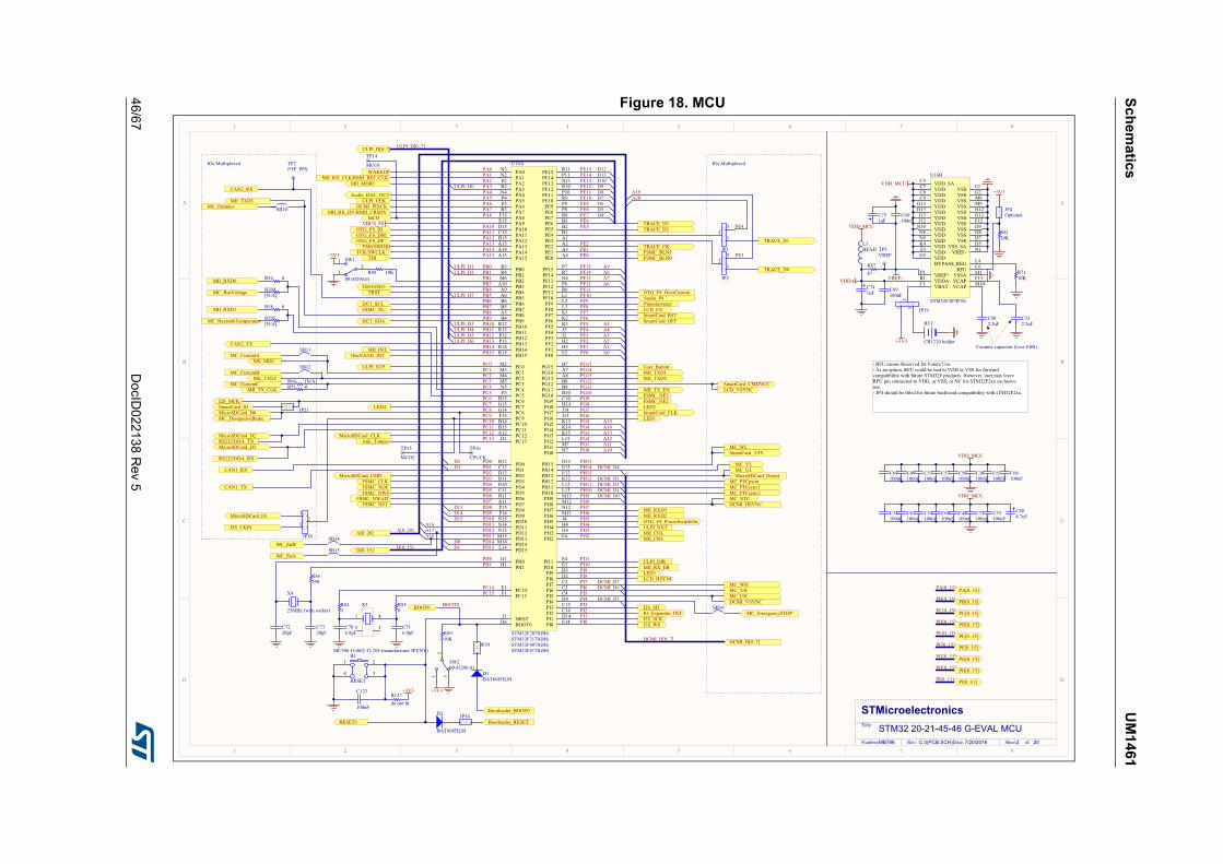
Figure 18. MCU
1
1
2
2
3
3
4
4
5
5
6
6
7
7
8
8
D D
C C
B B
A A
STMicroelectronicsTitle:
Number: Rev: Sheet ofC.3(PCB.SCH)Date:7/20/2016MB786 2 20
STM32 20-21-45-46 G-EVAL MCU
PA[0..15] PA[0..15]
PB[0..15] PB[0..15]
PC[0..15] PC[0..15]
PD[0..15] PD[0..15]
PE[0..15] PE[0..15]
1
4 3
2B1
RESET
R137do not fit
+3V3C123
100nF
C7320pF
C7220pF
X4
25MHz (with socket)
R86390
R8910K
+3V3
231
SW209.03290.01
RESET#
R88 10K
+3V3
23
1 SW1
09.03290.01
41
32
X3
MC306-G-06Q-32.768 (manufacturer JFVNY)
C716.8pF
C706.8pF
R850
R840
TP2PTP_PPS
Bootloader_BOOT0
Bootloader_RESET
DCMI_PIXCK
DCMI_VSYNC
DCMI_D[0..7]
DCMI_HSYNC
MCO
ULPI_D[0..7]
ULPI_CLK
ULPI_DIR
ULPI_NXT
ULPI_STP
RS232/IrDA_TX
RS232/IrDA_RX
OTG_FS_PowerSwitchOn
OTG_FS_OverCurrent
OTG_FS_DMOTG_FS_DP
OTG_FS_ID
I2S_WS
I2S_SD
I2S_SCK
I2S_MCK
Audio_DAC_OUT
CAN1_TX
CAN1_RX
CAN2_TX
CAN2_RX
MII_TXD0
MII_TX_ENMII_TX_CLK
MII_RXD0
MII_RX_ER
MII_RX_DV/RMII_CRSDV
MII_RX_CLK/RMII_REF_CLK
MII_COLMII_CRS
MII_MDC
MII_MDIO
MII_TXD1MII_TXD2
MII_TXD3
MII_RXD1
MII_RXD2MII_RXD3
MII_INT
LED4
LED3
LED1
LED2
Potentiometer
Anti_Tamper
WAKEUP
User_Button
I2C1_SCL
I2C1_SDA
IO_Expandor_INT
TDI
TRACE_D3TRACE_D2
TRACE_D1
TRACE_D0
TRACE_CK
TRST
TMS/SWDIOTCK/SWCLK
TDO/SWO
D[0..15]
A[0..20]
FSMC_NE3
MicroSDCard_CLK
MicroSDCard_CMD
MicroSDCard_D0
MicroSDCard_D1
MicroSDCard_D2
MicroSDCard_D3
MicroSDCard_Detect
MC_EmergencySTOP
MC_CurrentA
MC_CurrentB
MC_CurrentC
MC_PFCsync1MC_PFCsync2
MC_WL
MC_VH
MC_VL
MC_UH
MC_UL
MC_WH
MC_NTC
MC_DissipativeBrake
MC_PFCpwm
MC_EnA
MC_EnB
MC_HeatsinkTemperature
MC_BusVoltage
MC_EnIndex
SmartCard_3/5V
SmartCard_IO
SmartCard_RST
SmartCard_CLK
SmartCard_OFF
SmartCard_CMDVCC
FSMC_NE1
FSMC_NE2
FSMC_NWEFSMC_NOE
FSMC_BLN0FSMC_BLN1
FSMC_NWAIT
FSMC_CLK
FSMC_NL
OneNAND_INT
PE0PE1PE2
PE3
PE4PE5PE6PE7PE8PE9PE10PE11PE12PE13PE14PE15
PI0PI1PI2PI3PI4PI5PI6PI7PI8PI9PI10PI11
PC0PC1PC2PC3PC4PC5PC6PC7PC8PC9PC10PC11PC12PC13
PC14PC15
PF0PF1PF2PF3PF4PF5PF6PF7PF8PF9PF10PF11PF12PF13PF14PF15
A0A1A2A3A4A5
PA0PA1PA2PA3PA4PA5PA6PA7PA8
PA10PA11PA12PA13PA14PA15
PH0PH1
PH2PH3PH4PH5PH6PH7PH8PH9PH10PH11PH12PH13PH14PH15
ULPI_D0
ULPI_D1ULPI_D2
PB0PB1PB2PB3PB4PB5PB6PB7PB8PB9PB10PB11PB12PB13PB14PB15
A6A7A8A9
PG0PG1PG2PG3PG4PG5PG6PG7PG8PG9PG10PG11PG12PG13PG14PG15
A10A11
ULPI_D3
DCMI_D0DCMI_D1DCMI_D2DCMI_D3
PD0PD1PD2PD3PD4PD5PD6PD7PD8PD9PD10PD11PD12PD13PD14PD15
D13D14D15
D4D5D6D7D8D9D10D11D12
A16A17
D0D1
A12A13A14A15
DCMI_D4D2D3
DCMI_D5
DCMI_D6DCMI_D7
DCMI_D[0..7]
A[0..20]
D[0..15]
ULPI_D[0..7]
VBUS_FS
PF[0..15] PF[0..15]
PG[0..15] PG[0..15]
PH[0..15] PH[0..15]
PI[0..11] PI[0..11]
JP21
BT1
CR1220 holder
L3BEAD
C741uF
C69100nF
R8747
VDDA
VDD_MCU
VREF+
C68100nF
TP5VREF
12
3 JP19
+3V3
VDD_MCU
C60100nF
VDD_MCU
C48100nF
C37100nF
C35100nF
C54100nF
C67100nF
C34100nF
C57100nF
VDD_MCU
C56100nF
C36100nF
C61100nF
C66100nF
C53100nF
C49100nF
C65100nF
IOs MultiplexedIOs Multiplexed
ULPI_D4ULPI_D5ULPI_D6
ULPI_D7
R7110K
C751uF
BOOT0BOOT0
D1BAT60JFILM
JP29
D2
BAT60JFILM
TP14
MCO1
TP16
CPUCK
TP15
MCO2
A18
A19A20
Audio_IN
JP34
SB10
SB11
SB12
SB14
SB15
SB16
R34 0
R204[N/A]
R58 0
R205[N/A]
12
3
JP1
12
3
JP2
PE2 A2PE3 A1PE4 B1PE5 B2PE6 B3
PI8 D2
PC13D1
PC14E1
PC15F1
PI9 D3PI10 E3PI11 E4
PF0 E2PF1 H3PF2 H2PF3 J2PF4 J3PF5 K3PF6 K2PF7 K1PF8 L3PF9 L2PF10 L1
PH0G1
PH1H1
NRSTJ1
PC0M2
PC1M3
PC2M4
PC3M5
PA0N3
PA1N2
PA2P2
PH2 F4PH3 G4PH4 H4PH5 J4
PA3R2
PA4N4
PA5P4
PA6P3
PA7R3
PC4N5
PC5P5
PB0R5
PB1R4
PB2M6
PF11 R6PF12 P6PF13 N6PF14 R7PF15 P7
PG0 N7PG1 M7
PE7 R8PE8 P8PE9 P9PE10 R9PE11 P10PE12 R10PE13 N11PE14 P11PE15 R11
PB10R12
PB11R13
PH6 M11PH7 N12PH8 M12PH9 M13PH10 L13PH11 L12PH12 K12
PB12P12
PB13P13
PB14R14
PB15R15
PD8P15
PD9P14
PD10N15
PD11N14
PD12N13
PD13M15
PD14M14
PD15L14
PG2 L15PG3 K15PG4 K14PG5 K13PG6 J15PG7 J14PG8 H14PC6H15
PC7G15
PC8G14
PC9F14
PA8F15
PA9E15
PA10D15
PA11C15
PA12B15
PA13A15
PH13 E12PH14 E13PH15 D13
PI0 E14PI1 D14PI2 C14PI3 C13
PA14A14
PA15A13
PC10B14
PC11B13
PC12A12
PD0B12
PD1C12
PD2D12
PD3D11
PD4D10
PD5C11
PD6B11
PD7A11
PG9 C10PG10 B10PG11 B9PG12 B8PG13 A8PG14 A7PG15 B7
PB3A10
PB4A9
PB5A6
PB6B6
PB7B5
BOOT0D6
PB8A5
PB9B4
PE0 A4PE1 A3
PI4 D4PI5 C4PI6 C3PI7 C2
U16A
STM32F207IGH6
VBATC1
VSS F2
VDDF3
VSS G2
VDDG3 VREF- N1
VSSA M1VREF+P1
VDDAR1
BYPASS_REG L4
VDDK4
VSS M8
VDDN8
VSS M9
VDDN9
VCAP M10
VDDN10
VSS H12
VDDJ12
VSS_SA D5
VDDJ13 VSS G12VDDH13
VCAP F13
VSS F12
VDDG13
VSS D9
VDDC9
VSS D8
VDDC8
VSS D7
VDDC7
RFU C6
VDD_SAC5U16B
STM32F207IFT6
LCD_HSYNC
LCD_VSYNC
LCD_CS
R8110K
JP4
+3V3
12
3
JP16
I2S_CKIN
R51 0R66 [N/A]
C584.7uF
STM32F217IGH6STM32F407IGH6STM32F417IGH6
Optional
- RFU means Reserved for Future Use.- As an option, RFU could be tied to VDD or VSS for forward compatibility with future STM32F products. However, user may leave RFU pin connected to VDD, or VSS, or NC for STM32F2xx exclusive use.- JP4 should be fitted for future backward compatibility with sTM32F2xx.
C332.2uF
C502.2uF
Ceramic capacitor (Low ESR)
UM
14
61S
chem
atics
DocID
022138 R
ev 5
47/67
Figure 19. USB-OTG HS
1
1
2
2
3
3
4
4
D D
C C
B B
A A
STMicroelectronicsTitle:
Number: Rev: Sheet ofC.3(PCB.SCH) Date:7/20/2016MB786 3 20
STM32 20-21-45-46 G-EVAL USB OTG HS
ULPI_D[0..7]
ULPI_CLK
ULPI_D0ULPI_D1ULPI_D2ULPI_D3
ULPI_DIRULPI_NXT
ULPI_STP
C444.7uF
+5V
R3210K
+3V3
R28330
12
LD7Green12
LD8
Red
R29620
C254.7uF
GND2
IN5
EN4 OUT 1FAULT 3U4
STMPS2141STR@54
R5012K[1%]
VBUS1
DM2
DP3
ID4
GND5
Shield0 USB
_Micro-A
B re
ceptacle
CN9475900001VBUS_HS
C240.1uF
PI11PC0
PH4
PA3
PA5
PB0PB1PB10
+3V3
C390.1uF
C290.1uF
C430.1uFC42
0.1uFC314.7uF
C260.1uF
C4033pF
X2
26MHz
R551M
C4133pF
ULPI_D[0..7]
PB11PB12PB13PB5
ULPI_D4ULPI_D5ULPI_D6ULPI_D7
R3110K
R46 2K2
R61 0R62 0
R69 0
GND D2GND C5
PSW_N D4
VBUS F4
ID D3
VCC F3
DP D1DM C1
RESET_NC4
FAULT E2NXTD5
DIRE5
STPD6
CLOCKA4
VCC(I/O) B2
D7C6
D6B6
D5A6
D4A5
D3A3
D2A2
D1A1
D0B1
VCC(I/O) B5
XTAL2F6
XTAL1F5
REG1V8 E6REG_3V3 E3
RREF C2
CFG0 E1
NC F1
NC F2
GND E4
CFG1 B4
CFG2 B3
CHIP_SEL_NC3
U8
ISP1705AET
+3V3
R72[N/A]
+3V3
R70100K
JP31
+3V3
+3V3
C460.1uF
C470.1uF
C640.1uF
C1310.1uF
A1
A2
B1
B2
U10USBULC6-2F3
A1
A2
B1
B2
U12ESDA14V2-2BF3
3
2
1
T39013
R20747K
R206[N/A]
+3V3
RESET#
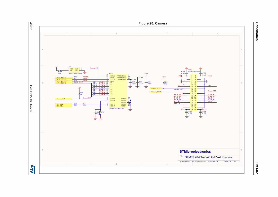
Sc
he
ma
tics
UM
146
1
48/6
7D
ocID022
138 Re
v 5
Figure 20. Camera
1
1
2
2
3
3
4
4
D D
C C
B B
A A
STMicroelectronicsTitle:
Number: Rev: Sheet ofC.3(PCB.SCH) Date:7/20/2016MB786 4 20
STM32 20-21-45-46 G-EVAL Camera
DCMI_PIXCKDCMI_VSYNC
DCMI_D[0..7]DCMI_HSYNC
Camera_RST
EN1 GND 2OUT 3VCC4U27
SM7745HEW-24.0M
+2V5
R13010K
DCMI_D[0..7] DCMI_D0DCMI_D1DCMI_D2DCMI_D3DCMI_D4DCMI_D5DCMI_D6DCMI_D7
R10810K
+2V8C900.1uF
I2C1_SCLI2C1_SDA
Camera_CLK
C840.1uF
DGND 1DGND 2
SIO_D3
AVDD(2.8V) 4
SIO_C5
RESET6
VSYNC7
PWDN8
HREF9
DVDD(1.8V) 10
DOVDD(2.8V) 11
Y712
XCLK113
Y614
DGND 15
Y516
PCLK17
Y418
Y019
Y320
Y121
Y222
AGND 23AGND 24
CN15
24-5805-024-000-829+
+2V8
JP26
C850.1uF
+1V8
+2V8
PH8PI5PA6
PB9PB6
PH9PH10PH11PH12
PI4PH14
PI6PI7
+2V8
R10910K
1 23 45 67 89 1011 1213 1415 1617 1819 2021 2223 2425 2627 2829 3031 3233 3435 3637 3839 40
CN23CLM-120-02-L-D
+1V8 +1V8
SCLSDA
SCL SDA
Camera_CLK
DCMI_D0 DCMI_D1DCMI_D2 DCMI_D3DCMI_D4 DCMI_D5DCMI_D6 DCMI_D7
HSYSCVSYSCPIXCLK
HSYSC VSYSCPIXCLK
+2V8 +2V8C1510.1uF
C1520.1uF
C1500.1uF
C1490.1uF
Camera_RST
Camera_RST
Camera_XSDN
+2V8
R21310K
Camera_PLUG

UM
14
61S
chem
atics
DocID
022138 R
ev 5
49/67
Figure 21. Ethernet
1
1
2
2
3
3
4
4
D D
C C
B B
A A
STMicroelectronicsTitle:
Number: Rev: Sheet ofC.3(PCB.SCH) Date:7/20/2016MB786 5 20
STM32 20-21-45-46 G-EVAL Ethernet
MII_TXD0MII_TX_EN
MII_TX_CLK
MII_RXD0
MII_RX_ER
MII_RX_DV/RMII_CRSDV
MII_RX_CLK/RMII_REF_CLK
MII_COL
MII_CRS
MII_MDCMII_MDIO
X125MHz (with socket)
C1422pF
C1522pF
12
3
JP5
MCO
EN1 GND 2OUT 3VCC4U3
SM7745HEV-50.0M (do not fit)
+3V3
R2610K
RESET#
R240
JP8R402K2
+3V3
+3V3
R254.87K
R30 2K2
+3V3R33 2K2
C210.1uF
C170.1uF
C190.1uF
C1310uF
R422K2
MII_TXD1
MII_TXD2MII_TXD3
MII_RXD1
MII_RXD2MII_RXD3
TX_CLK1
TX_EN2
TXD_03
TXD_14
TXD_25
TXD_3/SNI_MODE6
PWR_DOWN/INT7
NC 8NC 9NC 10NC 11NC 12RD- 13RD+ 14
AGND 15
TD- 16TD+ 17
PFBIN118
AGND 19
NC 20NC 21
AVDD33 22
PFBOUT23
RBIAS24
25MHz_OUT25
LED_ACT/COL/AN_EN 26LED_SPEED/AN1 27LED_LINK/AN0 28
RESET_N29
MDIO30 MDC31
IOVDD33 32X233
X134
IOGND 35
DGND 36
PFBIN237
RX_CLK38 RX_DV/MII_MODE39
CRS/CRS_DV/LED_CFG40
RX_ER/MDIX_EN41
COL/PHYAD042
RXD_0/PHYAD143
RXD_1/PHYAD244
RXD_2/PHYAD345
RXD_3/PHYAD446
IOGND 47
IOVDD33 48
U5
DP83848CVV
+3V3
C160.1uF
C270.1uF
C200.1uF
+3V3
R431.5K
12
3
JP6
TP125MHz
TD+1
TCT4
TD-2
RD+3
RCT5
RD-6
NC7
CHS GND8
LED(green)_A9
LED(green)_K10
LED(Yellow)_A12
LED(Yellow)_K11
Shield13
Shield14
CN7
J0011D21B
R22240
R1240
+3V3
C70.1uF
C60.1uF
+3V3MII_INT R41 0
R44 0 Second source: SI-60116-F
RS551
RS351
RS6
51
+3V3
Unused in RMII mode
RS1
2K2
RS451
RS2
51
PI10
PC1
PC2PC3
PA1
PA2
PH2
PH3
PA7PC4PC5
PG11
PH6PH7
PG13PG14
PB14
PB8
PA8
SB1
R20851
R212150
STM324xG-EVALSTM322xG-EVAL
SB1 R212CloseOpen
Not fitted150ohm
Board configuration
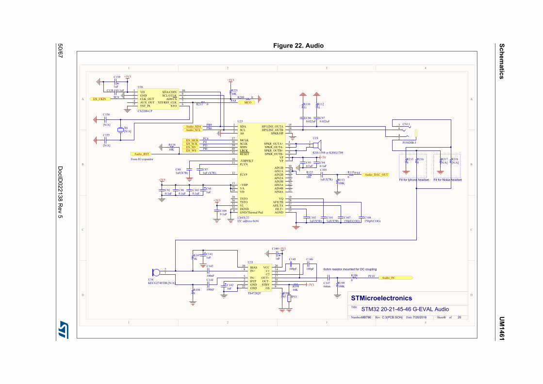
Sc
he
ma
tics
UM
146
1
50/6
7D
ocID022
138 Re
v 5
Figure 22. Audio
1
1
2
2
3
3
4
4
D D
C C
B B
A A
STMicroelectronicsTitle:
Number: Rev: Sheet ofC.3(PCB.SCH) Date:7/20/2016MB786 6 20
STM32 20-21-45-46 G-EVAL Audio
I2S_WSI2S_SDI2S_SCKR134
10K
Audio_SCLAudio_SDA
R11051
12
U19
KSS-1508 or KSSG1708Audio_RST
I2S_MCK
+5V
I2C address 0x94
C871uF (X7R)
C951uF
C1030.1uF
SDA1
SCL2
A03
SPKR_OUTA+ 4
VP 5
SPKR_OUTA- 6
SPKR_OUTB+ 7
VP 8SPKR_OUTB- 9
-VHPFILT10
FLYN11
FLYP12
+VHP13
HP/LINE_OUTB 14HP/LINE_OUTA 15
VA16
AGND 17FILT+ 18
VQ 19TSTO20
AIN4A 21AIN4B 22AIN3A 23AIN3B 24AIN2A 25AIN2B 26
AFILTA 27AFILTB 28
AIN1A 29AIN1B 30
SPKR/HP 31
RESET32
VL33
VD34
DGND35
TSTO36
MCLK37
SCLK38
SDIN39
LRCK40
GND/Thermal Pad0
U23
CS43L22
C881uF(X7R)
C980.1uF
C920.1uF
+2V5
C1040.1uF
+3V3
C1021uF(X5R)
C1011uF(X5R)
C107150pF(COG)
C108150pF(COG)
C940.1uF
C860.022uF
R11251
C970.022uF
C930.1uF
From IO expandor
Audio_DAC_OUTR122100
R113100K
C105
1uF(X7R)
R1150
PB9PB6
PC6
PI0
PI1PI3
PA4
Audio_INBYP2
GND4
IN-5
IN+8
GS 9
BIAS10
C1 14
C2 15
OUT- 16OUT+ 17
VCC 20
STBY 21
GND22
U33
TS472IQT
12
U34KECG2740TBL[N/A]
C143
100nF
R1980
C1411uF
R1971K
C144
100nFC1421uF
+3V3C140
1uF C145
100pF
C146
100pF
C1470ohm
R199100K
R1960
PF10
R20047
+3V3R19510K
JP33
2
6
4
3 CN11
PJ3028B-3
R2160
R2150
R217[N/A]
R218[N/A]
Fit for Iphone headset Fit for Nokia headset
VD1
GND2
CLK_OUT3
AUX_OUT4
TST_IN5 XTO 6XTI/REF_CLK 7AD0/CS 8SCL/CCLK 9SDA/CDIN 10U36
CS2200-CP
MCO
+3V3
C158 0.1uF
PA8I2S_CKIN
C159
1uF
PC9 R209 0
C155
[N/A]
C154
[N/A]X6[N/A]
R211 0
R22110K
+3V3
0ohm resistor mounted for DC coupling
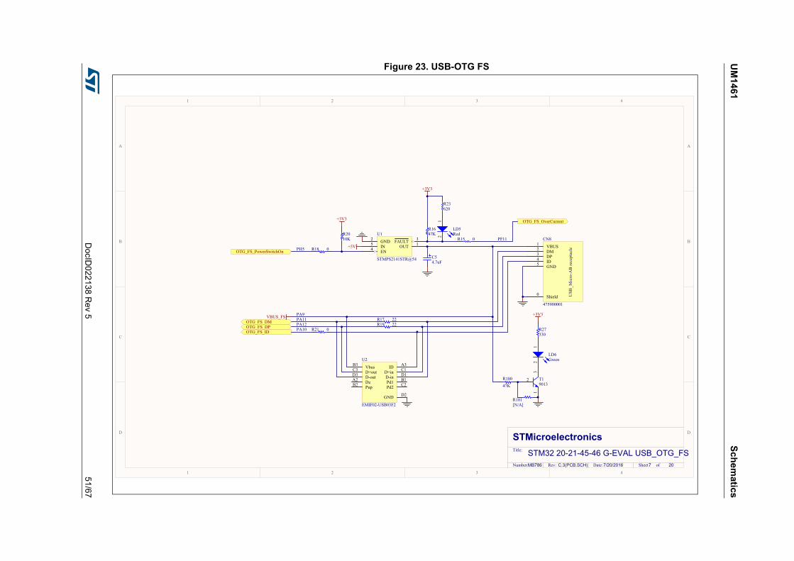
UM
14
61S
chem
atics
DocID
022138 R
ev 5
51/67
Figure 23. USB-OTG FS
1
1
2
2
3
3
4
4
D D
C C
B B
A A
STMicroelectronicsTitle:
Number: Rev: Sheet ofC.3(PCB.SCH) Date:7/20/2016MB786 7 20
STM32 20-21-45-46 G-EVAL USB_OTG_FS
+5V
R2010K
OTG_FS_PowerSwitchOn
OTG_FS_OverCurrent
R1647K
+3V3
12
LD5Red
R23620
OTG_FS_DMOTG_FS_DPOTG_FS_ID
C54.7uF
R18 0
R21 0
R15 0GND2
IN5
EN4 OUT 1FAULT 3U1
STMPS2141STR@54
VBUS1
DM2
DP3
ID4
GND5
Shield0 USB
_Micro-A
B re
ceptacle
CN8
475900001
VBUS_FS
PH5
PF11
PA9
PA10
PA11PA12
R17 22R19 22
DzA2
ID A3
Pd1 B1
PupB2
VbusB3
D+in C1
Pd2 C2
D+outC3
D-in D1
GND D2
D-outD3
U2
EMIF02-USB03F2
R27330
12
LD6Green
3
2
1
T19013
R18047K
+3V3
R181[N/A]
+3V3
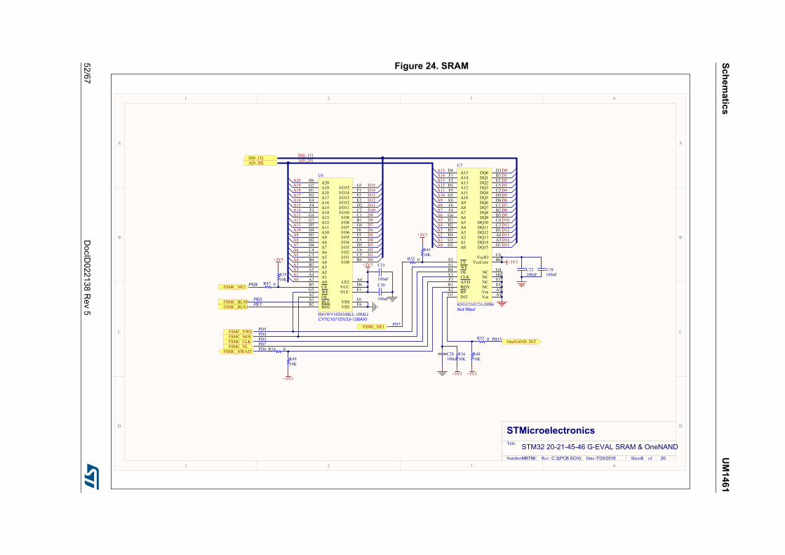
Sc
he
ma
tics
UM
146
1
52/6
7D
ocID022
138 Re
v 5
Figure 24. SRAM
1
1
2
2
3
3
4
4
D D
C C
B B
A A
STMicroelectronicsTitle:
Number: Rev: Sheet ofC.3(PCB.SCH) Date:7/20/2016
A1A2A3A4A5A6A7A8A9A10A11A12A13A14A15
A[0..20]D[0..15]
FSMC_NE1FSMC_NWEFSMC_NOE
FSMC_NWAIT
D[0..15]A[0..20]
R3610K
+3V3
A0
R4810K
C28100nF
+3V3
R4910K
+3V3
FSMC_CLKFSMC_NL
WEA1
RPA2
DQ14 A3
Vss A4Vss A5
DQ13 A6DQ12 B1
DQ8 B2
DQ1 B3
OEB4
DQ9 B5
VccCore B6
DQ7 C1
DQ4 C2
DQ11 C3DQ10 C4
DQ3 C5
VccIO C6
DQ15 D1
A12D2
DQ0 D3A15D4
DQ5 D5
DQ6 D6
CLKE1
CEE2
DQ2 E3
NC E4NC E5
A9E6
A14F1
A13F2
AVDF3
A7F4
A11F5
A8F6
INTG1
A0G2 A1G3
NC G4
A10G5
A6G6
RDYH1
A4H2 A5H3
A2H4 A3H5
NC H6
U7
KFG1216U2A-DIB6
C18100nF
C22100nF
+3V3R52 0
R4510K
+3V3
R53 0 OneNAND_INT
R54 0
MB786 8 20
STM32 20-21-45-46 G-EVAL SRAM & OneNAND
PD5PD4PD3PB7PD6
PD7
PB15
D0D1D2D3D4D5D6D7D8D9D10D11D12D13D14D15
A1A2A3A4A5A6A7A8A9A10A11A12A13A14A15A16
FSMC_NE2
FSMC_BLN0FSMC_BLN1
A0
A17
PE0PE1
R47 0
R3510K
+3V3
PG9
A18A19
C30
100nF
C23
100nF
+3V3D0D1D2D3D4D5D6D7D8D9D10D11D12D13D14D15
A20
CY7C1071DV33-12BAXI
A4B4
A3B3
A2A5
A1A4
A0A3
CEB5
I/O0 B6I/O1 C5I/O2 C6I/O3 D5
VCC D6
VSS D1
I/O4 E5I/O5 F5I/O6 F6I/O7 G6
WEG5
A16E4
A15F4
A14F3
A13G4
A12G3
A11H5
A10H4
A9H3
A8H2
I/O8 B1I/O9 C1I/O10 C2I/O11 D2
VCC E1
I/O12 E2I/O13 F2I/O14 F1I/O15 G1
BLEA1
BHEB2
OEA2
A7D4
A6C4
A5C3
A17D3 A18H1
VSS E6
A19G2 A20H6
CE2 A6
U6
IS61WV102416BLL-10MLINot fitted
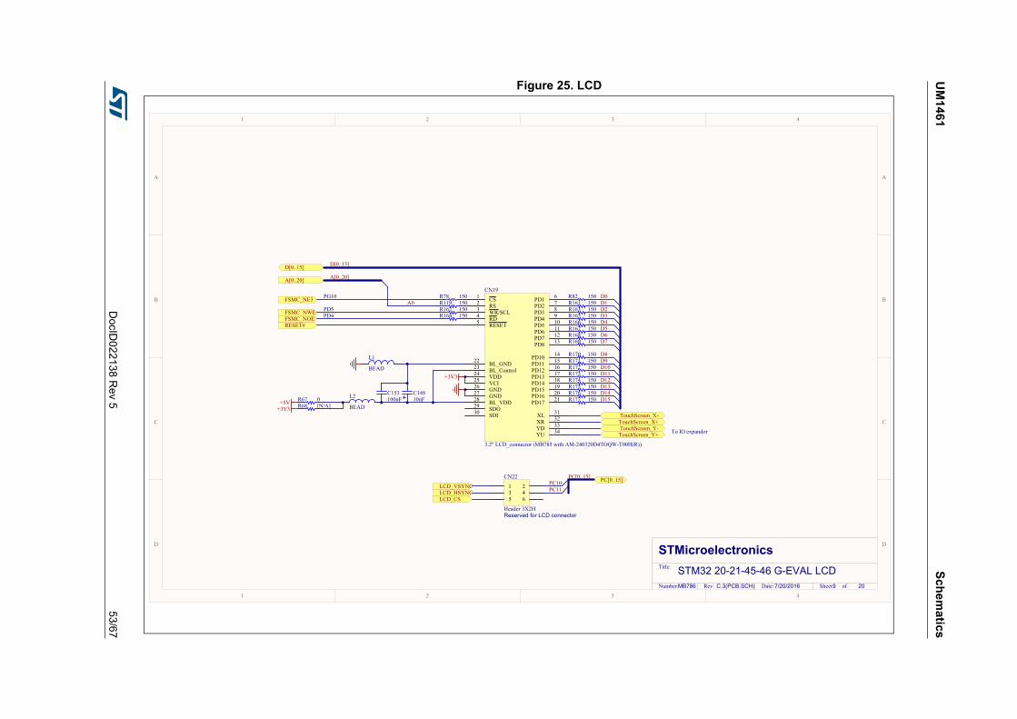
UM
14
61S
chem
atics
DocID
022138 R
ev 5
53/67
Figure 25. LCD
1
1
2
2
3
3
4
4
D D
C C
B B
A A
STMicroelectronicsTitle:
Number: Rev: Sheet ofC.3(PCB.SCH) Date:7/20/2016
TouchScreen_X+TouchScreen_X-
TouchScreen_Y+TouchScreen_Y-
CS1
RS2
WR/SCL3
RD4
RESET5
VDD24
VCI25
GND26
GND27
BL_VDD28
BL_Control23 BL_GND22
PD1 6
PD2 7
PD3 8
PD4 9
PD5 10
PD6 11
PD7 12
PD8 13
PD10 14
PD11 15
PD12 16
PD13 17
PD14 18
PD15 19
PD16 20
PD17 21
SDO29
SDI30 XL 31
XR 32
YD 33
YU 34
CN19
3.2" LCD_connector (MB785 with AM-240320D4TOQW-T00H(R))
+3V3
+5V
MB786 9 20
STM32 20-21-45-46 G-EVAL LCD
To IO expandor
RESET#
D[0..15]
A[0..20] A[0..20]
D[0..15]
FSMC_NWEFSMC_NOE
FSMC_NE3 D0D1D2D3D4D5D6D7
D8D9D10D11D12D13D14D15
A0PD5PD4
PG10
R170 150R171 150R172 150R173 150R174 150R175 150R176 150R177 150
R82 150R161 150R163 150R165 150R166 150R167 150R168 150R169 150
R78 150R119 150R162 150R164 150
C14810uFL2
BEAD
C153100nF
L1
BEAD
LCD_HSYNCLCD_VSYNC
LCD_CS
1 23 45 6
CN22
Header 3X2H
PC[0..15]PC10PC11
PC[0..15]
Reserved for LCD connector
R67 0
+3V3 R68 [N/A]
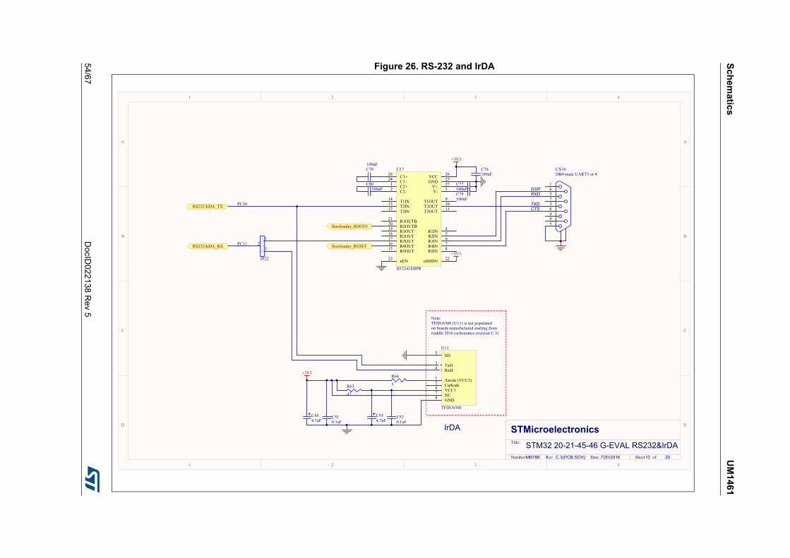
Sc
he
ma
tics
UM
146
1
54/6
7D
ocID022
138 Re
v 5
Figure 26. RS-232 and IrDA
1
1
2
2
3
3
4
4
D D
C C
B B
A A
STMicroelectronicsTitle:
Number: Rev: Sheet ofC.3(PCB.SCH) Date:7/20/2016
RS232/IrDA_TX
RS232/IrDA_RX
SD5
TxD3
GND8
Anode (VCC2)1
Cathode2
RxD4
VCC16
NC7
U11
TFDU6300
R64
5R63
47
C510.1uF
C520.1uF
+3V3
C554.7uF
C454.7uF
IrDA
32
1
JP22
MB786 10 20
STM32 20-21-45-46 G-EVAL RS232&IrDA
C2+1
C2-2 V- 3
R1IN 4
R2IN 5
R3IN 6
R4IN 7
R5IN 8
T1OUT 9
T2OUT 10
T3OUT 11T3IN12 T2IN13 T1IN14
R5OUT15 R4OUT16 R3OUT17 R2OUT18 R1OUT19 R2OUTB20 R1OUTB21
nSHDN 22nEN23
C1-24 GND 25VCC 26
V+ 27
C1+28U17
ST3241EBPR
C78100nF
C80100nF
C76100nF
C77100nFC79100nF
+3V3
162738495
CN16DB9-male UART3 or 4
+3V3
Bootloader_BOOT0
Bootloader_RESET
PC10
PC11
RXD
TXDCTS
DSR
TFDU6300 (U11) is not populatedon boards manufactured starting frommiddle 2016 (schematics revision C.3)
Note:
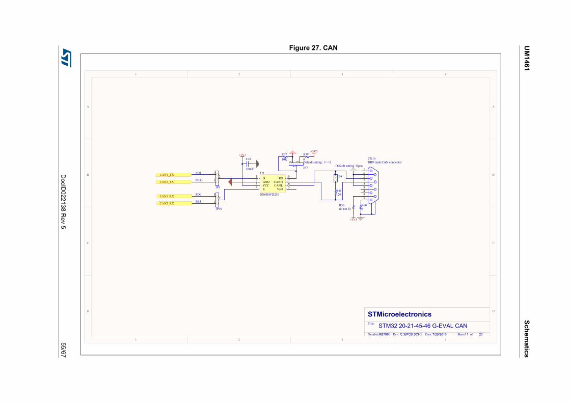
UM
14
61S
chem
atics
DocID
022138 R
ev 5
55/67
Figure 27. CAN
1
1
2
2
3
3
4
4
D D
C C
B B
A A
STMicroelectronicsTitle:
Number: Rev: Sheet ofC.3(PCB.SCH) Date:7/20/2016
CAN1_TX
CAN1_RX
D1
GND2
VCC3
R4 Vref 5CANL 6CANH 7RS 8U9
SN65HVD230
+3V3
+3V3
R38120
JP9
32
1
JP7
R3710K
+3V3
C32
100nF
R390
CAN2_TX
CAN2_RX R600
R56do not fit
Default setting: 1<->2Default setting: Open
MB786 11 20
STM32 20-21-45-46 G-EVAL CAN
162738495
CN10DB9-male CAN connector
PD1
PD0
PB13
PB5
32
1
JP3
32
1
JP10
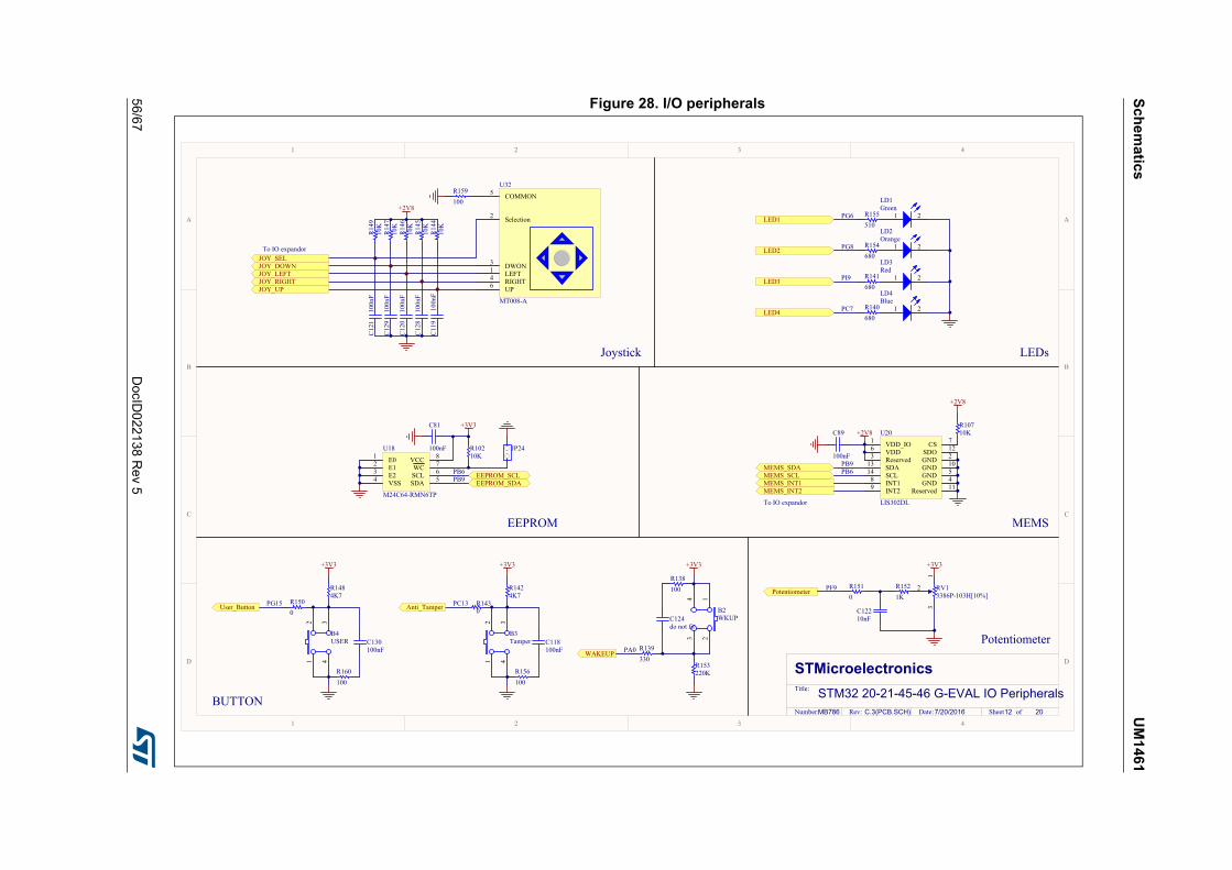
Sc
he
ma
tics
UM
146
1
56/6
7D
ocID022
138 Re
v 5
Figure 28. I/O peripherals
1
1
2
2
3
3
4
4
D D
C C
B B
A A
STMicroelectronicsTitle:
Number: Rev: Sheet ofC.3(PCB.SCH) Date:7/20/2016
1 2
LD3Red
1 2
LD2Orange
1 2
LD4Blue
1 2
LD1Green
R155510
R154680
R141680
R140680
LED4
LED3
LED1
LED2
31
2 RV13386P-103H[10%]
R1510
+3V3
Potentiometer
C12210nF
R14
710
KR14
610
KR14
510
KR14
410
K
R14
910
K
+2V8
C11
910
0nF
C12
810
0nF
C12
010
0nF
C12
910
0nF
C12
110
0nF
R159100
COMMON5
Selection2
DWON3
LEFT1
RIGHT4
UP6
U32
MT008-A
R153220K
143 2
B2WKUPC124
do not fit
+3V3
R138100R148
4K7
1 432
B4USER C130
100nF
+3V3
R160100
R1424K7
1 432
B3Tamper C118
100nF
+3V3
R156100
R139330
R1500
R1430
JOY_SELJOY_DOWNJOY_LEFTJOY_RIGHTJOY_UP
Anti_Tamper
WAKEUP
User_Button
EEPROM_SCLEEPROM_SDA
MEMS_SCLMEMS_SDA
MEMS_INT1MEMS_INT2
E01
E12
E23
VSS4 SDA 5SCL 6WC 7VCC 8U18
M24C64-RMN6TP
+3V3
R10210K
JP24 VDD_IO1
GND 2Reserved3
GND 4GND 5
VDD6 CS 7
INT18
INT29
GND 10
Reserved 11
SDO 12
SDA13
SCL14
U20
LIS302DL
+2V8R10710K
+2V8
MB786 12 20
STM32 20-21-45-46 G-EVAL IO Peripherals
Joystick LEDs
EEPROM MEMS
BUTTON
Potentiometer
C81
100nF
C89
100nF
To IO expandor
To IO expandor
R1521K
PG6
PG8
PI9
PC7
PC13
PA0
PG15
PF9
PB9PB6
PB9PB6
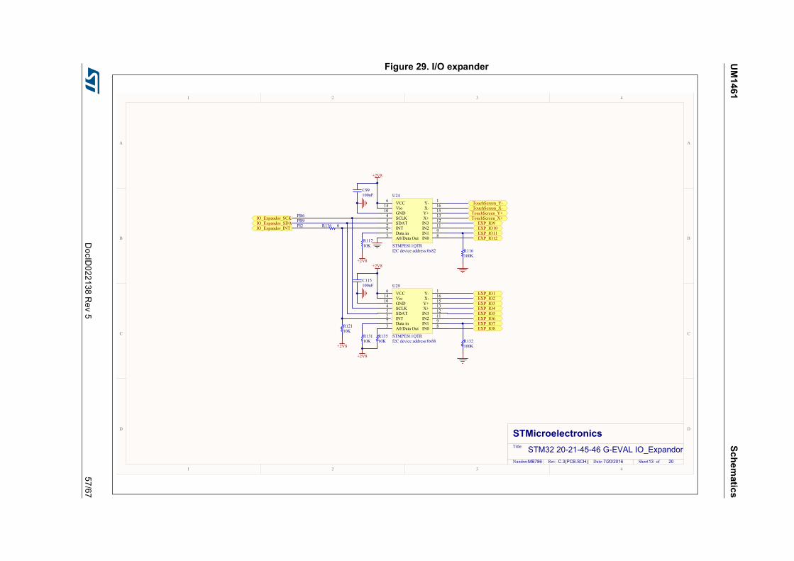
UM
14
61S
chem
atics
DocID
022138 R
ev 5
57/67
Figure 29. I/O expander
1
1
2
2
3
3
4
4
D D
C C
B B
A A
STMicroelectronicsTitle:
Number: Rev: Sheet ofC.3(PCB.SCH) Date:7/20/2016MB786 13 20
STM32 20-21-45-46 G-EVAL IO_Expandor
Y- 1
INT2
A0/Data Out3
SCLK4
SDAT5
VCC6
Data in7
IN0 8IN1 9
GND10
IN2 11IN3 12X+ 13
Vio14
Y+ 15X- 16
U24
STMPE811QTR
Y- 1
INT2
A0/Data Out3
SCLK4
SDAT5
VCC6
Data in7
IN0 8IN1 9
GND10
IN2 11IN3 12X+ 13
Vio14
Y+ 15X- 16
U29
STMPE811QTRR13510K
+2V8
I2C device address:0x82
I2C device address:0x88
+2V8
+2V8
R116100K
R132100K
IO_Expandor_SCKIO_Expandor_SDAIO_Expandor_INT
TouchScreen_X+
TouchScreen_X-TouchScreen_Y+
TouchScreen_Y-
EXP_IO2EXP_IO3EXP_IO4EXP_IO5EXP_IO6EXP_IO7EXP_IO8
EXP_IO9EXP_IO10EXP_IO11EXP_IO12
EXP_IO1
R12110K
R136 0
+2V8
R11710K
R13110K
+2V8
C99100nF
C115100nF
PB9PB6
PI2
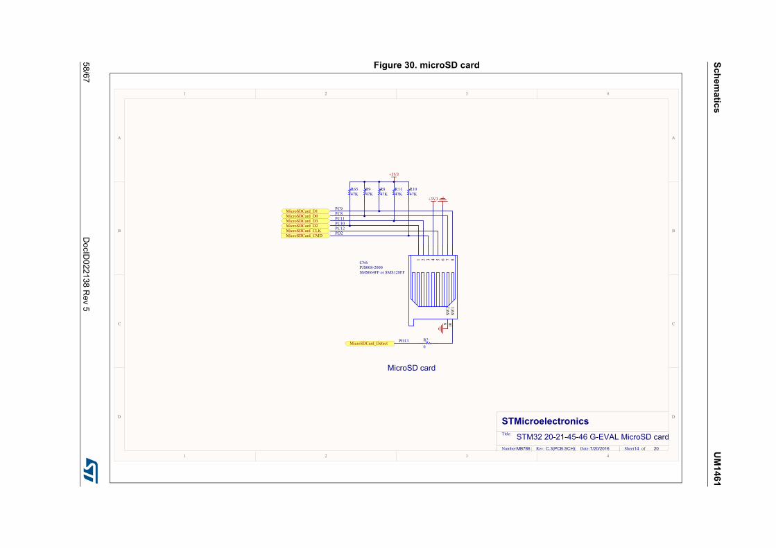
Sc
he
ma
tics
UM
146
1
58/6
7D
ocID022
138 Re
v 5
Figure 30. microSD card
1
1
2
2
3
3
4
4
D D
C C
B B
A A
STMicroelectronicsTitle:
Number: Rev: Sheet ofC.3(PCB.SCH) Date:7/20/2016
MicroSD card
MB786 14 20
STM32 20-21-45-46 G-EVAL MicroSD card
+3V3
MicroSDCard_CLKMicroSDCard_CMD
SMS064FF or SMS128FF
1 2 3 4 5 6 7 8SW
29
SW1
10
CN6PJS008-2000
MicroSDCard_D0MicroSDCard_D1
MicroSDCard_D2MicroSDCard_D3
MicroSDCard_Detect
R947K
R847K
R20
R1147K
R1047K
R6547K
+3V3
PC8PC9
PC10PC11
PC12PD2
PH13
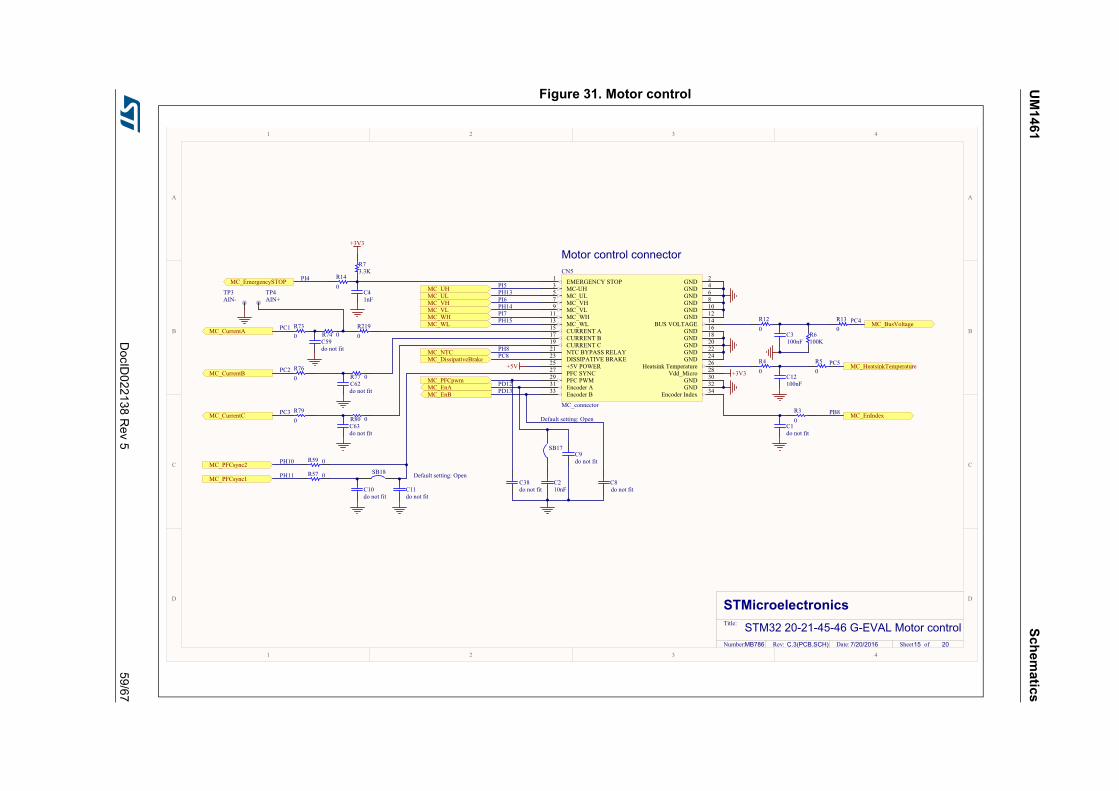
UM
14
61S
chem
atics
DocID
022138 R
ev 5
59/67
Figure 31. Motor control
1
1
2
2
3
3
4
4
D D
C C
B B
A A
STMicroelectronicsTitle:
Number: Rev: Sheet ofC.3(PCB.SCH) Date:7/20/2016
R73.3K
C41nF
+3V3
+3V3+5V
R140
C3100nF
C12100nF
R74 0C59do not fit
C62do not fit
C63do not fit
C11do not fit
C38do not fit
C210nF
C8do not fit
C1do not fit
R77 0
R80 0
R120
R40
C10do not fit
EMERGENCY STOP1
MC-UH3
MC_UL5
MC_VH7
MC_VL9
MC_WH11
MC_WL13
CURRENT A15
CURRENT C19 CURRENT B17
NTC BYPASS RELAY21
DISSIPATIVE BRAKE23
+5V POWER25
PFC SYNC27
PFC PWM29
Encoder A31
Encoder B33
GND 2
GND 4
GND 6
GND 8
GND 10
GND 12
BUS VOLTAGE 14
GND 16
GND 18
GND 20
GND 22
GND 24
Heatsink Temperature 26
Vdd_Micro 28
GND 30
GND 32
Encoder Index 34
CN5
MC_connector
MC_EmergencySTOP
MC_CurrentA
MC_CurrentB
MC_CurrentC
MC_PFCsync1
MC_PFCsync2
MC_WL
MC_VHMC_VL
MC_UHMC_UL
MC_WH
MC_NTCMC_DissipativeBrake
MC_PFCpwmMC_EnAMC_EnB
MC_HeatsinkTemperature
MC_BusVoltage
MC_EnIndex
R6100K
C9do not fit
Motor control connector
Default setting: Open
Default setting: Open
MB786 15 20
STM32 20-21-45-46 G-EVAL Motor control
R730
R760
R790
R130
R50
PC4
PC5
PC1
PC2
PC3
PH8
PH10
PH11
PD13
PC8
PB8
PH13
PH14
PH15
PD12
PI4PI5
PI6
PI7
R30
R59 0
R57 0
TP4AIN+
TP3AIN-
SB17
SB18
R2190
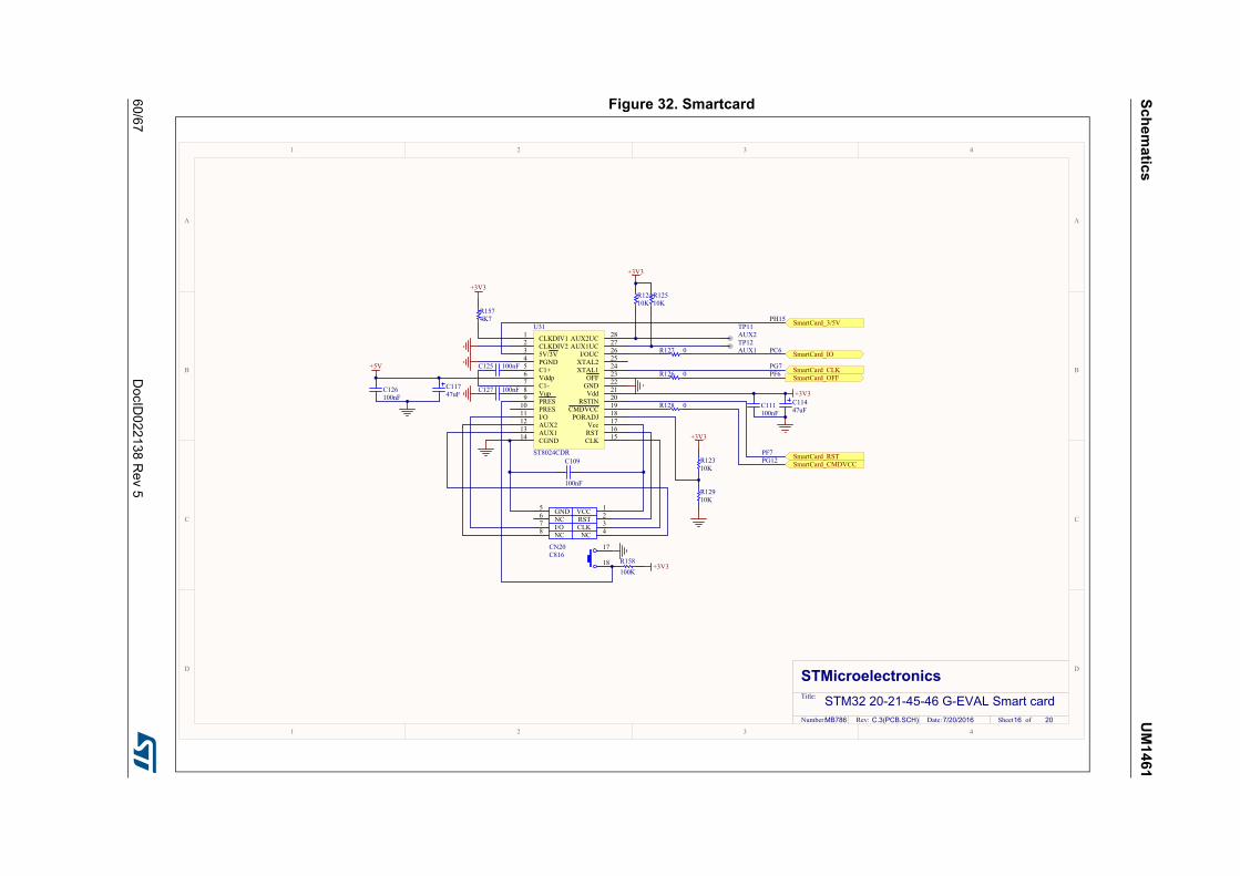
Sc
he
ma
tics
UM
146
1
60/6
7D
ocID022
138 Re
v 5
Figure 32. Smartcard
1
1
2
2
3
3
4
4
D D
C C
B B
A A
STMicroelectronicsTitle:
Number: Rev: Sheet ofC.3(PCB.SCH) Date:7/20/2016
VCC 1
RST 2
CLK 3
NC 4
GND5
NC6
I/O7
NC8
18
17CN20C816
CLKDIV11
CLKDIV22
5V/3V3
PGND4
C1+5
Vddp6
C1-7
Vup8
PRES9
PRES10
I/O11
AUX212
AUX113
CGND14 CLK 15RST 16Vcc 17PORADJ 18CMDVCC 19RSTIN 20Vdd 21GND 22OFF 23XTAL1 24XTAL2 25I/OUC 26AUX1UC 27AUX2UC 28U31
ST8024CDR
C125 100nF
C126100nF
C11747uF
+5V
C127 100nF
C109
100nF
R158100K
+3V3
R1574K7
+3V3
R12910K
R12310K
+3V3
C111100nF
C11447uF
+3V3
R12410K
+3V3
R127 0
R126 0
R12510K
TP11AUX2TP12AUX1
SmartCard_3/5V
SmartCard_IO
SmartCard_RST
SmartCard_CLKSmartCard_OFF
SmartCard_CMDVCC
MB786 16 20
STM32 20-21-45-46 G-EVAL Smart card
R128 0
PF7
PF6PG7
PC6
PG12
PH15
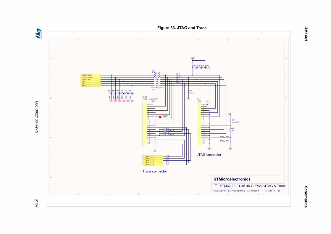
UM
14
61S
chem
atics
DocID
022138 R
ev 5
61/67
Figure 33. JTAG and Trace
1
1
2
2
3
3
4
4
D D
C C
B B
A A
STMicroelectronicsTitle:
Number: Rev: Sheet ofC.3(PCB.SCH) Date:7/20/2016
1234567891011121314151617181920
CN13FTSH-110-01-L-DV
+3V3
R97[N/A]
R96[N/A]
R101[N/A]
R95[N/A]
R98do not fit
+3V3
1234567891011121314151617181920
CN14JTAG +3V3
+3V3
R105 10K
R106 10K
R9910K
R92[N/A]
R1040R100do not fitR94 0R91 do not fit
TRACE_D3TRACE_D2TRACE_D1TRACE_D0TRACE_CK
Trace connector
JTAG connector
KEY
MB786 17 20
STM32 20-21-45-46 G-EVAL JTAG & Trace
PA13PA14PB3PA15PB4
PE6PE5PE4PE3PE2
TDI
RESET#TRST
TMS/SWDIOTCK/SWCLKTDO/SWO
D8
Z5V1
RS7
22D3
Z5V1
D4
Z5V1
D5
Z5V1
D6
Z5V1
D7
Z5V1
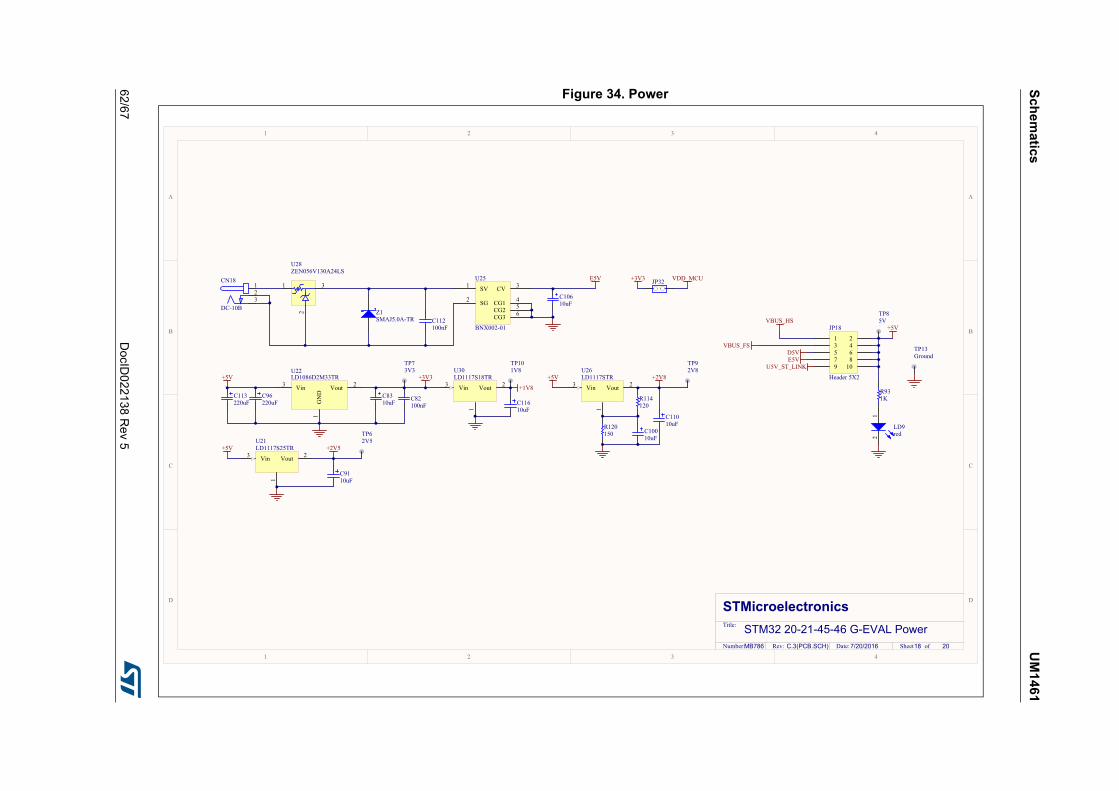
Sc
he
ma
tics
UM
146
1
62/6
7D
ocID022
138 Re
v 5
Figure 34. Power
1
1
2
2
3
3
4
4
D D
C C
B B
A A
STMicroelectronicsTitle:
Number: Rev: Sheet ofC.3(PCB.SCH) Date:7/20/2016
Vin3
GND
1
Vout 2
U22LD1086D2M33TR
C113220uF
C8310uF
C82100nF
+5V
TP73V3
SV1
SG2
CV 3
CG1 4
CG2 5
CG3 6
U25
BNX002-01
C10610uF
E5V
TP85V
+5V
R931K
12
LD9red
TP13Ground
1
32
CN18
DC-10BZ1SMAJ5.0A-TR C112
100nF
1
2
3
U28ZEN056V130A24LS
+3V3
D5VE5V
MB786 18 20
STM32 20-21-45-46 G-EVAL Power
Vin3 Vout 2
1
U21LD1117S25TR+5V
C9110uF
+2V5
TP62V5
C96220uF
VBUS_FS
VBUS_HS
Vin3 Vout 2
1
U30LD1117S18TR
C11610uF
+1V8 Vin3 Vout 2
1
U26LD1117STR+5V
C11010uF
+2V8
TP92V8
R114120
C10010uF
R120150
TP101V8
+3V3 VDD_MCUJP32
1 23 45 67 89 10
JP18
Header 5X2
U5V_ST_LINK
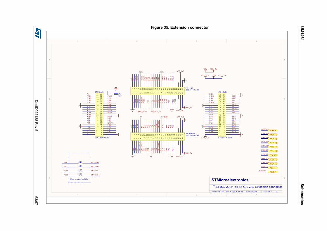
UM
14
61S
chem
atics
DocID
022138 R
ev 5
63/67
Figure 35. Extension connector
1
1
2
2
3
3
4
4
D D
C C
B B
A A
STMicroelectronicsTitle:
Number: Rev: Sheet ofC.3(PCB.SCH) Date:7/20/2016
RESET# RESET#
MB786 19 20
STM32 20-21-45-46 G-EVAL Extension connector
12345678910
111213141516171819202122232425262728293031323334353637383940
CN4
21N22564-40S10B 12
34
56
78
910
1112
1314
1516
1718
1920
2122
2324
2526
2728
2930
3132
3334
3536
3738
3940
4142
4344
4546
4748
4950
CN121N22564-50S10B 12
345678910
111213141516171819202122232425262728293031323334353637383940
CN2
21N22564-40S10B
12
34
56
78
910
1112
1314
1516
1718
1920
2122
2324
2526
2728
2930
3132
3334
3536
3738
3940
4142
4344
4546
4748
4950
CN321N22564-50S10B
PA0
PA1
PA2
PA3PA4PA5PA6PA7
PA8
PA10
PA11
PA12
PA13
PA14 PA15
PB0PB1PB2
PB3 PB4PB5 PB6PB7
PB8PB9
PB10PB11
PB12
PB13
PB14
PB15
PC0
PC1
PC2
PC3
PC4PC5
PC6
PC7
PC8
PC9
PC10 PC11PC12
PC13
EXT_
PC14
EXT_
PC15
PD0PD1 PD2
PD3PD4 PD5PD6 PD7
PD8
PD9
PD10
PD11
PD12
PD13
PD14
PD15
PE0PE1
PE2
PE3
PE4
PE5
PE6
PE7PE8PE9PE10PE11PE12PE13PE14PE15
PF0
PF1
PF2
PF3
PF4
PF5
PF6
PF7
PF8
PF9
PF10
PF11PF12PF13PF14PF15
PG0PG1
PG2
PG3
PG4
PG5
PG6
PG7
PG8
PG9 PG10PG11 PG12PG13PG14 PG15
EXT_
PH0
EXT_
PH1
PH2
PH3
PH4
PH5
PH6PH7PH8PH9PH10
PH11
PH12
PH13
PH14
PH15
PI0
PI1
PI2
PI3
PI4PI5 PI6PI7
PI8
PI9
PI10
PI11
VREF+
EMU_3V3
EMU_5V
APP_3V3
APP_VCCPC
13RES
ET#
EMU_5V EMU_3V3
EMU_5V
APP_3V3
BOOT0
(Left) (Right)
(Buttom)
(Top)
PA[0..15] PA[0..15]
PB[0..15] PB[0..15]
PC[0..15] PC[0..15]
PD[0..15] PD[0..15]
PE[0..15] PE[0..15]
PF[0..15] PF[0..15]
PG[0..15] PG[0..15]
PH[0..15] PH[0..15]
PI[0..11] PI[0..11]
APP_3V3APP_VCC
EMU_5VD5V
+3V3
SB6
SB7
SB4
SB5
PH0
PH1
PC14
PC15
EXT_PH0
EXT_PH1
EXT_PC14
EXT_PC15
Close to crystal on PCB
BOOT0BOOT0
VBUS_FS
CX133pF
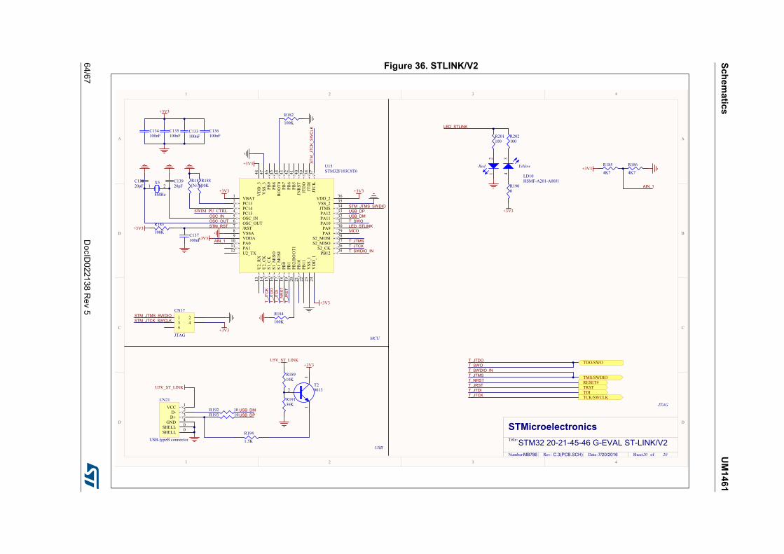
Sc
he
ma
tics
UM
146
1
64/6
7D
ocID022
138 Re
v 5
Figure 36. STLINK/V2
1
1
2
2
3
3
4
4
D D
C C
B B
A A
STMicroelectronicsTitle:
Number: Rev: Sheet ofC.3(PCB.SCH) Date:7/20/2016 20 20
VBAT1
PC132
PC143
PC154
OSC_IN5
OSC_OUT6
/RST7
VSSA8
VDDA9
PA010
PA111
U2_TX12
U2_
RX
13
U2_
CK
14
S1_C
K15
S1_M
ISO
16
S1_M
OSI
17
PB0
18
PB1
19
PB2/BOOT1
20
PB10
21
VSS
_123
VDD_1
24
PB12 25
PB11
22
S2_CK 26S2_MISO 27S2_MOSI 28PA8 29PA9 30PA10 31PA11 32PA12 33JTMS 34VSS_2 35VDD_2 36
JTCK
37JT
DI
38JT
DO
39JN
RST
40PB
541
PB6
42PB
743
BOOT0
44PB
845
PB9
46VSS
_347
VDD_3
48
U15STM32F103C8T6
20pFC139
20pFC138
1 2X5
8MHz+3V3
USB_DMUSB_DP
STM_RST
T_JT
CK
T_JTCK
T_JT
DO
T_JT
DI
T_JTMS
STM_JTMS_SWDIO
STM
_JTC
K_S
WCLK
LED_STLINK
OSC_INOSC_OUT
T_NRST
T_JR
ST
LED_STLINK
T_JTCKT_JTDI
T_JTDO
T_NRSTT_JTMS
T_JRST
R185
4K7
R186
4K7
AIN_1C137100nF
R183
100K
R201100
+3V3
+3V3
+3V3+3V3
+3V3
+3V3
AIN_1
VCC 1
D- 2
D+ 3
GND 4
SHELL 0
SHELL 0
CN21
USB-typeB connector
USB_DMUSB_DP
+3V3
C135100nF
C133100nF
C136100nF
C134100nF
R192 10R193 10
MCU
USB
JTAG
STM_JTMS_SWDIOSTM_JTCK_SWCLK
+3V3
U5V_ST_LINKTDITRST
TMS/SWDIO
TCK/SWCLK
TDO/SWO
RESET#
SWIM_PU_CTRL
R182
100K
T_SWOT_SWDIO_IN
T_SWDIO_IN
T_SWO
1 23 45
CN17
JTAG
R194
1.5K
R18910K
R19136K
2
31
T29013
+3V3U5V_ST_LINK
R187[N/A]
R18810K
R184
100K
MCO
21 4
3
Red Yellow
LD10HSMF-A201-A00J1
R202100
R1900
+3V3
MB786
STM32 20-21-45-46 G-EVAL ST-LINK/V2

UM
14
61S
chem
atics
DocID
022138 R
ev 5
65/67
Figure 37. 3.2” LCD module with SPI and 16-bit interface
1
1
2
2
3
3
4
4
D D
C C
B B
A A
STMicroelectronicsTitle:
Number: Rev: Sheet ofA.1(PCB.SCH) Date:3/27/2009
EnableDotClkHSYNCVSYNC
CS
RS
WRRD
#RESET
SDOSDI
VDD
PD0PD1PD2PD3PD4PD5PD6PD7PD8PD9PD10PD11PD12PD13PD14PD15PD16PD17
YUYDXRXL
VSS1
XL 2XR 3YD 4YU 5
VSS6
IM0/ID 7
IM1 8
IM3 9
SDO10
NC11
SDI12
D17 13D16 14D15 15D14 16D13 17D12 18D11 19D10 20D9 21D8 22D7 23D6 24D5 25D4 26D3 27D2 28D1 29D0 30CS31
RESET32
RS33
WR/SCL34
RD35
VSYNC36
HSYNC37
DOTCLK38
ENABLE39
VCC40
VCC41
VSS42
LED_K43 LED_A44
VSS45
CN2
FF0245SS1
R4 0
R1 10K VDD
RP1
10KRP2
10K
RP4
10K
PD0
PD2PD4PD6PD8
PD9
PD10
PD11
PD12
PD13
PD14
PD15
PD16
PD17
Enable
DotClk
HSYNC
VSYNC
VDD
C31uF/50V
R3 4K7R2 4K7
SDISDO
RDRS
Soldered for Serial interface only
Soldered for i80-system 16-bit interface
The 34-pin connector to mother board for both serial & 16bit interface. Compatible with MB694 with Touch screen signals added on Pin 31-34.
CSRSWRRD#RESET
VDD
BLGND
BLVDD
BL_Control
PD1PD2PD3PD4PD5PD6PD7PD8
PD10PD11PD12PD13PD14PD15PD16PD17
SDOSDI
AK
Z1
STPS1L40M C14.7uF/50V
L1
4.7uH(1A)
R710
BLGND
BLVDD
R6100K
C22.2uF
R50
R8do not fit
BLVDD
BL_Control
BLGND
BLGND
BLGND
AM-240320D4TOQW-T00H(R)
Vi1
Rset 2GND3 FB 4
NC 5Vo 6
EN7
SW8
PGND9
U1
STLD40DPMR
CS1
RS2
WR/SCL3
RD4
RESET5
VDD24
VCI25
GND26
GND27
BL_VDD28
BL_Control23 BL_GND22
PD1 6
PD2 7
PD3 8
PD4 9
PD5 10
PD6 11
PD7 12
PD8 13
PD10 14
PD11 15
PD12 16
PD13 17
PD14 18
PD15 19
PD16 20
PD17 21
SDO29
SDI30 XL 31
XR 32
YD 33
YU 34
CN1
3.2LCD_connector
YUYDXRXL
LCD board connector to Mother board
MB785 1 1
3.2" LCD module with both SPI & 16bit interface
RP3
10K
RP6
10K
RP5
10K
PD1PD3PD5PD7

Revision history UM1461
66/67 DocID022138 Rev 5
Revision history
Table 35. Document revision history
Date Revision Changes
02-Sept-2011 1 Initial release.
09-Oct-2011 2Updated Table 5 JP24 description. Added warning in Chapter 2.5 and note in Chapter 2.16 and Chapter 2.20.
09-Jan-2012 3Added note in Chapter 2.5 and updated Chapter Appendix A: Schematics.
06-Apr-2012 4 Added note in Section 2.20.
27-Oct-2016 5
Added the following feature update throughout the document: IrDA transceiver is only supported up to version C07 of the board (no more supported from board version C08). Updated in Introduction, Features, Hardware layout and configuration and RS-232 and IrDA as well as in Figure 2 and Figure 3.
Figure 17 to Figure 37 changed.

DocID022138 Rev 5 67/67
UM1461
67
IMPORTANT NOTICE – PLEASE READ CAREFULLY
STMicroelectronics NV and its subsidiaries (“ST”) reserve the right to make changes, corrections, enhancements, modifications, and improvements to ST products and/or to this document at any time without notice. Purchasers should obtain the latest relevant information on ST products before placing orders. ST products are sold pursuant to ST’s terms and conditions of sale in place at the time of order acknowledgement.
Purchasers are solely responsible for the choice, selection, and use of ST products and ST assumes no liability for application assistance or the design of Purchasers’ products.
No license, express or implied, to any intellectual property right is granted by ST herein.
Resale of ST products with provisions different from the information set forth herein shall void any warranty granted by ST for such product.
ST and the ST logo are trademarks of ST. All other product or service names are the property of their respective owners.
Information in this document supersedes and replaces information previously supplied in any prior versions of this document.
© 2016 STMicroelectronics – All rights reserved
Related Documents