National Aeronautics and Space Administration Single-Event Gate Rupture and Single- Event Burnout Test Results Performed on Hi-Rel Fuji Power MOSFETs: 2SK4217, 2SK4152, 2SK4155, and 2SK4158 Luis E. Selva, Ph.D. Jet Propulsion Laboratory Pasadena, California Jet Propulsion Laboratory California Institute of Technology Pasadena, California JPL Publication 09-26 10/09

Welcome message from author
This document is posted to help you gain knowledge. Please leave a comment to let me know what you think about it! Share it to your friends and learn new things together.
Transcript

National Aeronautics and Space Administration
Single-Event Gate Rupture and Single-Event Burnout Test Results Performed on Hi-Rel Fuji Power MOSFETs: 2SK4217,
2SK4152, 2SK4155, and 2SK4158
Luis E. Selva, Ph.D. Jet Propulsion Laboratory
Pasadena, California
Jet Propulsion Laboratory California Institute of Technology
Pasadena, California
JPL Publication 09-26 10/09


National Aeronautics and Space Administration
Single-Event Gate Rupture and Single-Event Burnout Test Results Performed on Hi-Rel Fuji Power MOSFETs: 2SK4217,
2SK4152, 2SK4155, and 2SK4158
NASA Electronic Parts and Packaging (NEPP) Program Office of Safety and Mission Assurance
Luis E. Selva, Ph.D. Jet Propulsion Laboratory
Pasadena, California
NASA WBS: 939904.01.11.30 Project Number: 103982 Task Number: 03.04.03
Jet Propulsion Laboratory
4800 Oak Grove Drive Pasadena, CA 91109
http://nepp.nasa.gov

This research was carried out at the Jet Propulsion Laboratory, California Institute of
Technology, and was sponsored by the National Aeronautics and Space Administration
Electronic Parts and Packaging (NEPP) Program.
Reference herein to any specific commercial product, process, or service by trade name,
trademark, manufacturer, or otherwise, does not constitute or imply its endorsement by the
United States Government or the Jet Propulsion Laboratory, California Institute of
Technology.
Copyright 2009. California Institute of Technology. Government sponsorship acknowledged.

i
Executive Summary Several newly available Hi-Rel total dose hardened power metal-oxide-semiconductor
field-effect transistors (MOSFETs) manufactured by Fuji Electric Device Technology Co. Ltd (FDT) in conjunction with the Japan Aerospace Exploration Agency (JAXA) were tested for single-event gate rupture (SEGR) and single-event burnout (SEB). The safe-operating area (SOA) of the 2SK4217 (a 100 V rated device), 2SK4152 (130 V), 2SK4155 (200 V), and 2SK4158 (250 V) MOSFETs were tested with silver (Ag) and xenon (Xe) ions having incident linear energy transfers (LETs) of 42.2 and 53.1 MeV cm2/mg, respectively. Test results show these devices are comparable to currently available total dose hardened technology.
It is recommended that reliability testing be undertaken for these device types, i.e., infant mortality, lifetime testing and dose-history effects on SEGR/SEB. The resulting information could be valuable information for spacecraft designers.
ii
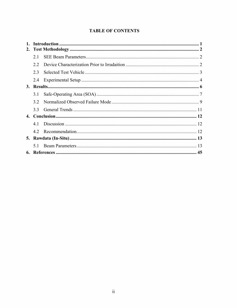
TABLE OF CONTENTS
1. Introduction ........................................................................................................................ 1 2. Test Methodology ............................................................................................................... 2
2.1 SEE Beam Parameters ................................................................................................. 2
2.2 Device Characterization Prior to Irradaition ............................................................... 2
2.3 Selected Test Vehicle .................................................................................................. 3
2.4 Experimental Setup ..................................................................................................... 4 3. Results.................................................................................................................................. 6
3.1 Safe-Operating Area (SOA) ........................................................................................ 7
3.2 Normalized Observed Failure Mode ........................................................................... 9
3.3 General Trends .......................................................................................................... 11 4. Conclusion ......................................................................................................................... 12
4.1 Discussion ................................................................................................................. 12
4.2 Recommendation ....................................................................................................... 12 5. Rawdata (In-Situ) ............................................................................................................. 13
5.1 Beam Parameters ....................................................................................................... 13 6. References ......................................................................................................................... 45

1
1. Introduction The metal-oxide-semiconductor field-effect transistor (MOSFET) is the most widely used
transistor onboard a spacecraft. The MOSFET is typically employed in digital and analog circuits. It is a device designed to route or switch electrical power and is typically utilized to regulate high voltages and currents, i.e., from hundreds to several thousand volts (V) and up to a hundred amperes (A). On board a spacecraft, power MOSFETs are used as part of a multiplex bus architecture, where microcontrollers and or actuators are used for initiating a predetermined set of events, i.e., deploying a parachute, firing retrorockets, etc. Devices like power MOSFETs are sensitive to heavy ion irradiation and can fail catastrophically as a result of single-event gate rupture (SEGR), or single-event burnout (SEB). Manufacturers design radiation-hardened power MOSFETs for space applications. These radiation-hardened devices are not impervious to SEGR or SEB, but rather can succumb to them at a much larger linear energy transfer (LET) than their non-radiation hardened counterparts.
Over the last two decades, spacecraft designers have seen a reduction in the number of manufacturers that produce radiation-hardened power MOSFETs. In 1994, Nichols et al. [1] indicated that out of the eight manufacturers whose power MOSFETs were tested by the radiation community at large, only three were producing radiation-hardened power MOSFETs. In the mid-1990s [2–3] that number had decreased to only two, and in recent years only one manufacturer has produced for Hi-Rel space applications.
Recently, Fuji Electric Device Technology Co. Ltd (FDT) in conjunction with the Japan Aerospace Exploration Agency (JAXA) developed a radiation-hardened n-channel power MOSFET. The voltage ratings for these devices range from 100 V to 500 V. The technology was presented at the 17th Microelectronics Workshop in 2004 and has undergone Qualification Testing (QT) in accordance with JAXA requirements [4]. Some data has been presented as in [5], but data tested to an acceptable NASA standard has yet to be presented. In this study, we present data taken according to the current NASA test standards [6]. The devices tested are the 2SK4217 (a 100 V rated device), 2SK4152 (130 V), 2SK4155 (200 V), and 2SK4158 (250 V) radiation-hardened power MOSFETs (100 krad).
This document is organized as follows: Section 1 provides an introduction; Section 2 discusses the single-event effects (SEE) beam parameters, device characterization, selected test vehicle, experimental setup, bias conditions during irradiation, failure condition, and error analysis; Section 3 describes the results, the safe-operating area (SOA), the observed failure modes (OFM), two examples, and a brief observation on the general trend; Section 4 presents and describes the conclusion, discussion, and recommendation of the study; Section 5 contains the raw data, i.e., graphs and figures; and Section 6 contains the references.
2
2. Test Methodology 2.1 SEE Beam Parameters
All SEE tests were conducted in accordance with reference [6]. All devices were tested at the Texas A&M University (TAMU) Cyclotron Facility. The ions selected for the experiment had a range greater than the thickness of the epitaxial layer of all test devices (>107 µm in silicon). The ions used were silver (Ag) and xenon (Xe) with an ion energy of 15 MeV/amu. The incident LET of the ion-beam post-aramic film and column of air was determined by TAMU and can be found at the following website: http://cyclotron.tamu.edu/ref/beams.php. For each irradiation, the device under test (DUT) was exposed to ~1×10⁵ ions/cm2 at a flux of ~1×10⁴ ions/cm2 per second; thus, each irradiation run lasted ~10 seconds.
2.2 Device Characterization Prior to Irradaition Prior to any irradiation, the devices were electrically characterized using a Tektronix 371b
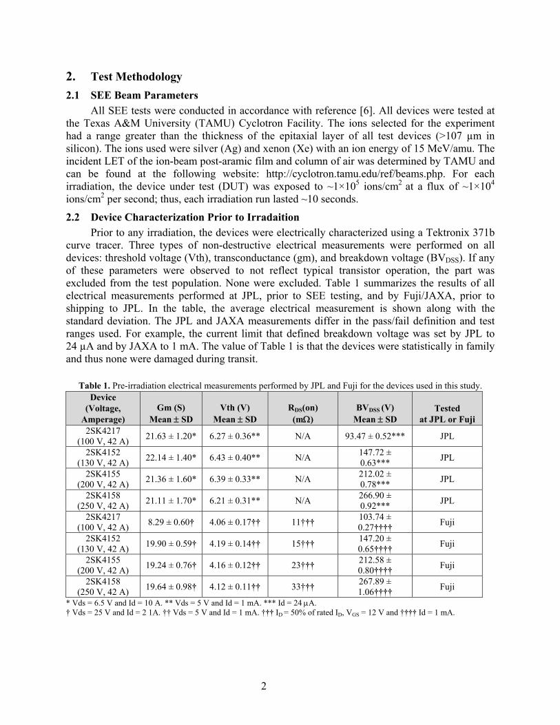
curve tracer. Three types of non-destructive electrical measurements were performed on all devices: threshold voltage (Vth), transconductance (gm), and breakdown voltage (BVDSS). If any of these parameters were observed to not reflect typical transistor operation, the part was excluded from the test population. None were excluded. Table 1 summarizes the results of all electrical measurements performed at JPL, prior to SEE testing, and by Fuji/JAXA, prior to shipping to JPL. In the table, the average electrical measurement is shown along with the standard deviation. The JPL and JAXA measurements differ in the pass/fail definition and test ranges used. For example, the current limit that defined breakdown voltage was set by JPL to 24 µA and by JAXA to 1 mA. The value of Table 1 is that the devices were statistically in family and thus none were damaged during transit.
Table 1. Pre-irradiation electrical measurements performed by JPL and Fuji for the devices used in this study.
Device (Voltage,
Amperage) Gm (S)
Mean ± SD Vth (V)
Mean ± SD RDS(on)
(mΩ) BVDSS (V)
Mean ± SD Tested
at JPL or Fuji 2SK4217
(100 V, 42 A) 21.63 ± 1.20* 6.27 ± 0.36** N/A 93.47 ± 0.52*** JPL
2SK4152 (130 V, 42 A) 22.14 ± 1.40* 6.43 ± 0.40** N/A 147.72 ±
0.63*** JPL
2SK4155 (200 V, 42 A) 21.36 ± 1.60* 6.39 ± 0.33** N/A 212.02 ±
0.78*** JPL
2SK4158 (250 V, 42 A) 21.11 ± 1.70* 6.21 ± 0.31** N/A 266.90 ±
0.92*** JPL
2SK4217 (100 V, 42 A) 8.29 ± 0.60† 4.06 ± 0.17†† 11††† 103.74 ±
0.27†††† Fuji
2SK4152 (130 V, 42 A) 19.90 ± 0.59† 4.19 ± 0.14†† 15††† 147.20 ±
0.65†††† Fuji
2SK4155 (200 V, 42 A) 19.24 ± 0.76† 4.16 ± 0.12†† 23††† 212.58 ±
0.80†††† Fuji
2SK4158 (250 V, 42 A) 19.64 ± 0.98† 4.12 ± 0.11†† 33††† 267.89 ±
1.06†††† Fuji
* Vds = 6.5 V and Id = 10 A. ** Vds = 5 V and Id = 1 mA. *** Id = 24 μA. † Vds = 25 V and Id = 2 1A. †† Vds = 5 V and Id = 1 mA. ††† ID = 50% of rated ID, VGS = 12 V and †††† Id = 1 mA.

3
2.3 Selected Test Vehicle The tested devices were packaged in the SMD-2 configuration with a die size of one block
per one unit, i.e., 1/1. The block can be split into one, two, or four units. Splitting the block into one or more units effectively results in lowering the current capability of the fabricated device and increasing the maximum-on resistance (RDS(on)) for a given voltage rating (Table 1).
Figure 1 shows the pre-irradiation measurements performed at JPL on all the devices (shown by device type). The series of graphs in Figure 1 show the transfer curve for each device type. The transconductance and threshold voltage were determined by the transfer curve. The error bars represent the standard deviation within the tested population, and are caused by a large part-to-part variation within each device type. Temperature was not monitored during these measurements. However, the threshold voltage and transconductance (slope of curves) were consistent between parts.
Figure 1. Pre-irradiation electrical measurements (i.e., transconductance and threshold voltage for each device type).

4
Figure 2. Schematic of experimental setup.
2.4 Experimental Setup Figure 2 shows the schematic of the experimental setup used during the SEE testing. All
devices were biased and measured with the HP4142B Modular DC Source/Monitor Unit (SMU) connected to a personal computer (PC) via a general-purpose instrument bus (GPIB). The current and voltage changes were measured at approximately 100 ms increments; the maximum current resolution of the SMU was 1 nA. Background noise in a virgin device typically had an amplitude of 60 nA. The manufacturer sent the devices without packaging for SEE testing.
2.4.1 Bias Conditions During Irradiation During heavy ion exposure, test devices were continuously monitored for leakage currents
through the gate, source, and drain terminals at a constant gate-to-source voltage (VGS) and a constant drain-to-source voltage (VDS). Between irradiations, the device was biased to ensure that no latent damage had occurred, but only at the previously irradiated bias, which is a variance from [6]. If the DUT was still operational, the voltage was increased and the device was irradiated again. Bias conditions during irradiation consisted of VGS held constant, with VDS incremented at each exposure until catastrophic failure.
2.4.2 Failure Condition SEGR was defined as the drain-to-source voltage at which the current from gate-to-drain or
gate-to-source permanently exceeded 1 μA; this variable is called Vcrit. The mean SEGR voltage value was determined by computing the arithmetic average of the “last pass” voltage and the voltage at “failure.” Since the definition of the SEGR voltage is the average voltage at which the DUT exhibited an SEE and the voltage of the previous irradiation, a valid data point is one where the DUT exhibited no failures (SEGR or SEB) for at least one complete irradiation run. One type of SEGR occurs when the gate and drain currents exceed 1 µA; the source current is not altered by the catastrophic event, i.e., the large current is from gate to drain. SEGR can also manifest itself as high gate and source currents that exceed 1 µA, while the drain stays intact. SEB, on the other hand, exhibits a high source to drain current. The functionality of the gate is retained following the event. However, current control is no longer possible as the properties of the semiconductor have been damaged.
5
2.4.3 Error Bars The voltage steps (system resolution, SR) were chosen to be 5% of the device voltage
rating. The error bars associated with each data point on the safe-operating area (SOA) curve were computed by taking the square root of the sum of the squares of the uncertainty in each measurement (SR) and the standard deviation (SD) of all measurements on multiple device samples performed at the specific VDS and VGS bias condition.
2.4.4 Part Inventory In order to map out the entire SOA of a power MOSFET for a given LET, many devices
had to be tested destructively. Thirty parts per device type were available for testing. The parts were divided into two equal groups for each LET. Each group was subdivided into four groups of three parts. The four groups of three parts were used to test the following bias (VGS) conditions: 0 V, −5 V, −10 V, and−15 V. Six parts were kept in reserve. Thus, a strategy was formulated whereby we could maximize the amount of information that could be acquired from the viable parts.
6
3. Results Overall, the radiation response of these devices yielded comparable SEE responses as
currently available total ionizing dose (TID)-hardened power MOSFETs. Device electrical characterization performed prior to irradiation yielded a part-to-part variation of less than 10% (see Section 4.1). SEE variability, defined as part-to-part variation under identical test conditions, ranged from 0% to ~41% (see Section 4.1). The greatest SEE variability was observed for the 53.1 MeV cm2/mg incident ion.
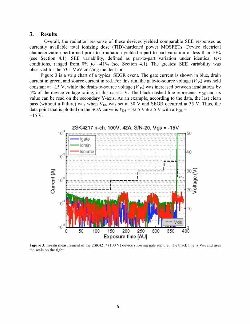
Figure 3 is a strip chart of a typical SEGR event. The gate current is shown in blue, drain current in green, and source current in red. For this run, the gate-to-source voltage (VGS) was held constant at −15 V, while the drain-to-source voltage (VDS) was increased between irradiations by 5% of the device voltage rating, in this case 5 V. The black dashed line represents VDS and its value can be read on the secondary Y-axis. As an example, according to the data, the last clean pass (without a failure) was when VDS was set at 30 V and SEGR occurred at 35 V. Thus, the data point that is plotted on the SOA curve is VDS = 32.5 V ± 2.5 V with a VGS = −15 V.
Figure 3. In-situ measurement of the 2SK4217 (100 V) device showing gate rupture. The black line is VDS and uses the scale on the right.

7
3.1 Safe-Operating Area (SOA) Figures 4a through 4d show the SOA curves of the four Hi-Rel Fuji devices tested. Not
surprisingly, the larger LET reduced the SOA. The Vcrit value decreases as gate-to-source bias decreases, which is typical of non-SEE hardened parts. These results are comparable to similar devices tested in previous studies [7]. No significant anomalies were seen in any of the test data; however, the frequency of latent damage events (that is, SEGR events that result in gate leakage currents below the SEGR definition) was observed to be higher than previous data [8].
Figure 4a. SOA curves for the 2SK4217 (100 V) radiation-hardened power MOSFET tested using long-range ions with incident LETs of 42.2 and 53.1 MeV cm2/mg.

8
Figure 4b. SOA curves for the 2SK4152 (130 V) radiation-hardened power MOSFET tested using long-range ions with incident LETs of 42.2 and 53.1 MeV cm2/mg.
Figure 4c. SOA curves for the 2SK4155 (200 V) radiation-hardened power MOSFET tested using long-range ions with incident LETs of 42.2 and 53.1 MeV cm2/mg.

9
Figure 4d. SOA curves for the 2SK4158 (250 V) radiation-hardened power MOSFET tested using long-range ions with incident LETs of 42.2 and 53.1 MeV cm2/mg.
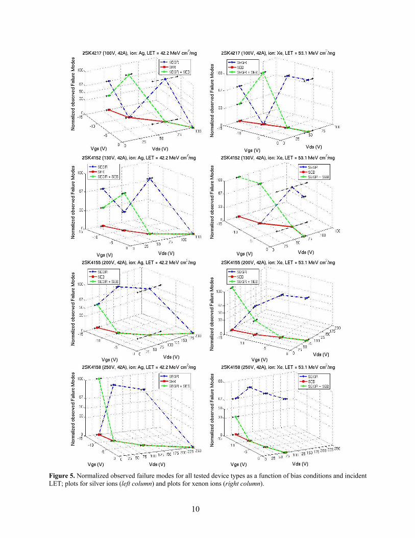
3.2 Normalized Observed Failure Mode In order to depict the relative frequency of SEB and SEGR, plots of the event frequency are
shown in 3D format. These plots allow for analysis of what SEE type dominates for various operation conditions, and for investigation of how the SOA depends on the operation mode. These plots, which are similar to Schmoo plots, are valuable in evaluating new technologies like these. For example, when designing an SEB resistant circuit, knowing which operation conditions are likely to enhance SEB or SEGR, can be easily be determined from Figure 5.
Figure 5 plots the normalized failure modes (SEGR, SEB, and SEGR+SEB) that were observed for each of the tested device types for a range of bias conditions and incident LETs. The SEGR+SEB failure mode is not an arithmetic superposition of SEGR and SEB, but rather a failure where SEGR and SEB occur simultaneously. The left column in Figure 5 displays plots for silver ions, and the right column displays plots for xenon ions. The X- and Y-axis correspond to the applied bias conditions (VGS and VDS) seen on the SOA curves. Error bars are shown in the VDS (Y-axis) only. The Z-axis represents the normalized observed failure modes (in percent) for the sampled devices at the applied VGS and VDS bias. The Z-axis represents the normalized observed failure modes (in percent) for the sampled devices at the applied VGS and VDS bias.
10
Figure 5. Normalized observed failure modes for all tested device types as a function of bias conditions and incident LET; plots for silver ions (left column) and plots for xenon ions (right column).

11
3.2.1 Example 1, No Failure below VDS Rating When VGS = 0V The first example highlights the condition where the device did not experience a failure
below its rated voltage (VDS) when VGS was set to zero. On the top left plot of Figure 5 (2SK4217, LET = 42.2 MeV cm2/mg), VDS was systematically increased from zero volts up to the rated voltage (100 V) and no SEGR or SEB or a combination of SEGR and SEB (SEGR+SEB) were observed. Thus, the percent of failure as a result of SEGR or SEB or SEGR+SEB was zero. As VGS was decreased, we observed the onset of various failure modes. At VGS of −5.0 V, all of the devices failed below the rated voltage with a clear signature of SEGR. The failures occurred for VDS between 60.5 V and 94.5 V. At VGS of −10.0 V, none of the devices failed through SEGR, but rather through SEGR+SEB. At VGS of −15.0 V, 67% of the devices failed through SEGR and 33% via SEGR+SEB. These failures occurred for VDS between 30.0 V and 35.0 V. SEB was never observed as a single failure mode, instead it was always found in conjunction with SEGR, i.e., SEGR+SEB.
3.2.2 Example 2, Failure Below VDS Rating When VGS = 0V The second example highlights the condition where the device experiences a failure well
below its rated voltage when VGS was set to zero. On the top right plot of Figure 5 (2SK4217, LET = 53.1 MeV cm2/mg), at VGS of 0 V, all of the devices failed below the rated voltage with a clear signature of SEGR. The failures occurred for VDS between 45.5 V and 53.0 V. As VGS was decreased, we observed the onset of the SEGR+SEB failure mode. At VGS of −10 V all of the devices failed through SEGR+SEB. These failures occurred for VDS between 35.4 V and 43.0 V. At VGS of −15.0 V, 67% of the devices failed through SEGR and 33% via SEGR+SEB. These failures occurred for VDS between 25.4 V and 33.0 V. SEB was never observed as a single failure mode, instead it was always found in conjunction with SEGR, i.e., SEGR+SEB.
3.3 General Trends Figure 5 displays some obvious trends. All of the devices were immune to SEE at VGS =
0.0 V when tested with silver ions (LET = 42.2 MeV cm2/mg). SEGR and SEGR+SEB failure modes were more likely to occur for both Ag and Xe ions when VGS was set below 0 V. As mentioned previously, SEB was never observed as a single failure mode, but rather in concert with SEGR, i.e., SEGR+SEB.
Another observed trend revealed that failed devices irradiated while under relatively low bias conditions (VGS = 0 V and −5 V) were found to still be partially operational; that is, the devices were leaky (IG ~10 μA). This trend was not observed for devices irradiated under VGS values of −10 V and −15 V.

12
4. Conclusion SEGR and SEB test results of the Fuji power MOSFETs that have emerged onto the
catalog of available devices show that these devices yield comparable SEE responses as power MOSFETs devices that are TID hardened.
4.1 Discussion Following electrical characterization, we defined part-to-part variability as the quotient
between the standard deviation and mean value, e.g., (SD)/(mean electrical value). Table 2 shows the results. Electrical variability was below 10% for all device types tested.
SEE variability was computed as described above. The SEE variability is tabulated in Table 3 for the tested device types as a function of incident ion LET and bias condition. In Table 3, the grey highlighted area denotes SEE variability in excess of 10% (arbitrarily cutoff). Note that for the explored bias space (from VGS of 0 V to –15 V), SEE variability increased with LET for a given device type. For example, for the 2SK4217 device irradiated with Ag ions, the number of boxes whose SEE variability exceeded 10% was 1. While, under Xe irradiation, the number of grey boxes with SEE variability of over 10% was 2. The reason behind the increase of SEE variability with LET is presently not clear and may need to be investigated in the future.
4.2 Recommendation It is recommended that reliability testing be undertaken for these device types, i.e., infant
mortality, lifetime testing, and dose-history effects on SEGR/SEB. Results from those experiments would provide a wealth of valuable information to spacecraft designers. Table 2. Part-to-part variability results, calculation based on electrical measurements conducted at JPL prior to SEE testing.
Device (Voltage, Amperage) Threshold Voltage Variability
between Parts (%) Transconductance Variability
between Parts (%)
2SK4217 (100 V, 42 A) 6.3 5.5
2SK4152 (130 V, 42 A) 6.3 6.3
2SK4155 (200 V, 42 A) 5.2 7.5
2SK4158 (250 V, 42 A) 4.8 8.1
Table 3. SEE part-to-part variability results, calculations based on heavy ion irradiations (SEE measurements) conducted at Texas A&M Cyclotron Facility.
Device (Voltage,
Amperage)
LET (Ag) = 42.2 MeV cm2/mg LET (Xe) = 53.1 MeV cm2/mg
VGS = 0 V VGS = -5 V VGS = -10 V VGS = -15 V VGS = 0 V VGS = -5 V VGS = -10 V VGS = -15 V
2SK4217 (100 V, 42 A) 0.0% 23.1% 8.5% 7.7% 14.8% 7.8% 9.8% 13.1%
2SK4152 (130 V, 42 A) 0.0% 27.3% 6.7% 9.1% 4.7% 5.9% 7.8% 11.1%
2SK4155 (200 V, 42 A) 0.0% 38.4% 9.1% 16.6% 10.8% 12.4% 18.3% 14.3%
2SK4158 (250 V, 42 A) 0.0% 37.7% 11.1% 14.8% 7.7% 11.1% 14.3% 24.1%
13
5. Rawdata (In-Situ) Data acquired during all irradiations are listed here by device type and bias condition.
5.1 Beam Parameters Two types of energetic heavy ions were used to acquire the data in this section—silver
(Ag) ions with beam energy of 1289 MeV, with an incident LET of 42.2 MeV cm2/mg, and a range in silicon (Si) of 119.3 µm; and xenon (Xe) ions with beam energy of 1366 MeV, with an incident LET of 53.1 MeV cm2/mg, and a range in Si of 107.7 µm. During all irradiations, the fluence step was maintained at ~1×10⁵ ions/cm2.
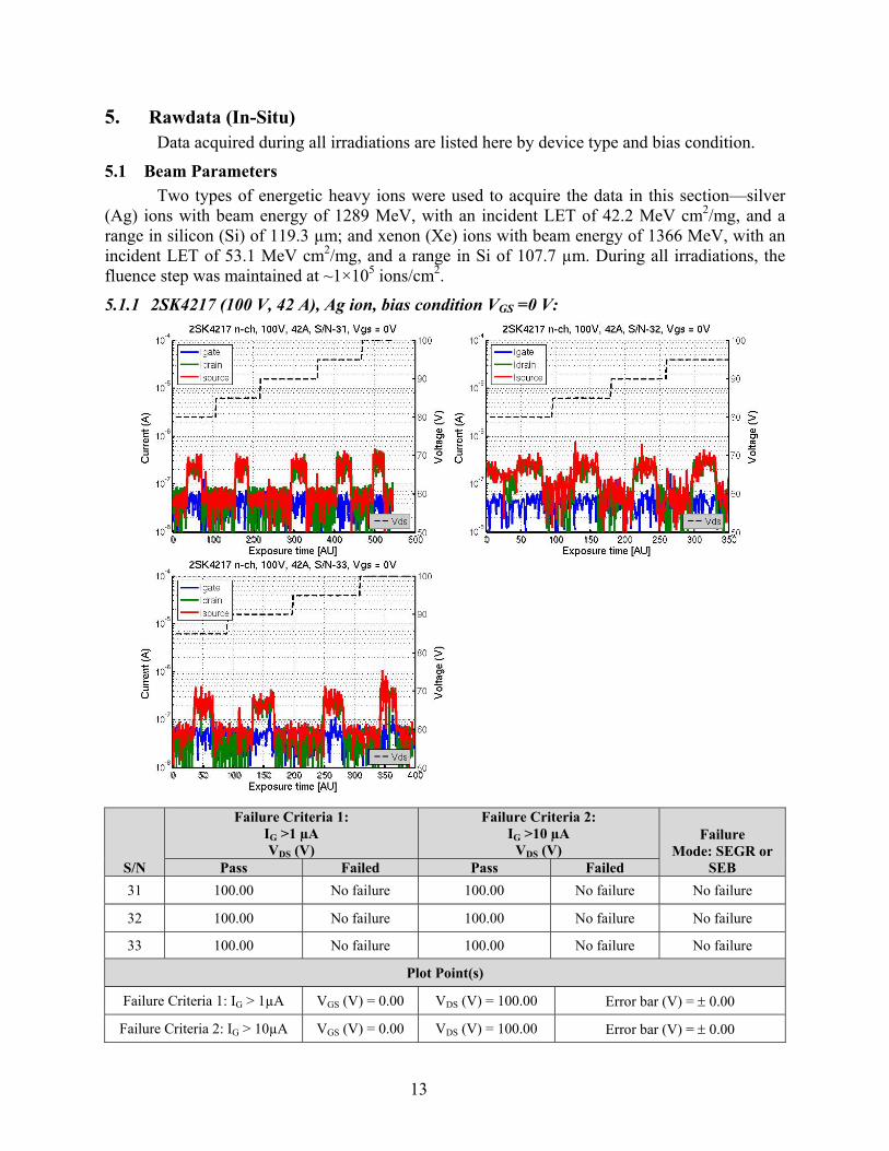
5.1.1 2SK4217 (100 V, 42 A), Ag ion, bias condition VGS =0 V:
S/N
Failure Criteria 1: IG >1 µA VDS (V)
Failure Criteria 2: IG >10 µA
VDS (V) Failure
Mode: SEGR or SEBPass Failed Pass Failed
31 100.00 No failure 100.00 No failure No failure
32 100.00 No failure 100.00 No failure No failure
33 100.00 No failure 100.00 No failure No failure
Plot Point(s)
Failure Criteria 1: IG > 1µA VGS (V) = 0.00 VDS (V) = 100.00 Error bar (V) = ± 0.00
Failure Criteria 2: IG > 10µA VGS (V) = 0.00 VDS (V) = 100.00 Error bar (V) = ± 0.00

14
5.1.2 2SK4217 (100 V, 42 A), Ag ion, bias condition VGS = −5 V:
S/N
Failure Criteria 1: IG >1 µA VDS (V)
Failure Criteria 2: IG >10 µA
VDS (V) Failure
Mode: SEGR or SEBPass Failed Pass Failed
26 55.00 60.00 75.00 80.00 SEGR
35 80.00 85.00 95.00 100.00 SEGR
28 70.00 75.00 90.00 95.00 SEGR
30 100.00 No failure 100.00 No failure No failure
Plot Point(s)
Failure Criteria 1: IG > 1 µA VGS (V) = −5.00 VDS (V) = 78.13 Error bar (V) = ± 18.01
Failure Criteria 2: IG > 10 µA VGS (V) = −5.00 VDS (V) = 91.88 Error bar (V) = ± 10.08

15
5.1.3 2SK4217 (100 V, 42 A), Ag ion, bias condition VGS = −10 V:
S/N
Failure Criteria 1: IG >1 µA VDS (V)
Failure Criteria 2: IG >10 µA
VDS (V) Failure
Mode: SEGR or SEB Pass Failed Pass Failed
22 45.00 50.00 45.00 50.00 SEGR & SEB
23 40.00 45.00 40.00 45.00 SEGR & SEB
25 40.00 45.00 45.00 50.00 SEGR & SEB
34 45.00 50.00 45.00 50.00 SEGR & SEB
Plot Point(s)
Failure Criteria 1: IG > 1 µA VGS (V) = −10.00 VDS (V) = 45.00 Error bar (V) = ± 3.82
Failure Criteria 2: IG > 10 µA VGS (V) = −10.00 VDS (V) = 46.25 Error bar (V) = ± 3.54

16
5.1.4 2SK4217 (100 V, 42 A), Ag ion, bias condition VGS = −15 V:
S/N
Failure Criteria 1: IG >1 µA VDS (V)
Failure Criteria 2: IG >10 µA
VDS (V) Failure
Mode: SEGR or SEB Pass Failed Pass Failed
19 30.00 35.00 30.00 35.00 SEGR & SEB
20 30.00 35.00 30.00 35.00 SEGR
21 30.00 35.00 30.00 35.00 SEGR
Plot Point(s)
Failure Criteria 1: IG >1 µA VGS (V) = −15.00 VDS (V) = 32.50 Error bar (V) = ± 2.50
Failure Criteria 2:IG >10 µA VGS (V) = −15.00 VDS (V) = 32.50 Error bar (V) = ± 2.50
17
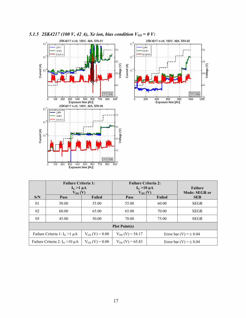
5.1.5 2SK4217 (100 V, 42 A), Xe ion, bias condition VGS = 0 V:
S/N
Failure Criteria 1: IG >1 µA VDS (V)
Failure Criteria 2: IG >10 µA
VDS (V) Failure
Mode: SEGR or SEB Pass Failed Pass Failed
01 50.00 55.00 55.00 60.00 SEGR
02 60.00 65.00 65.00 70.00 SEGR
05 45.00 50.00 70.00 75.00 SEGR
Plot Point(s)
Failure Criteria 1: IG >1 µA VGS (V) = 0.00 VDS (V) = 54.17 Error bar (V) = ± 8.04
Failure Criteria 2: IG >10 µA VGS (V) = 0.00 VDS (V) = 65.83 Error bar (V) = ± 8.04

18
5.1.6 2SK4217 (100 V, 42 A), Xe ion, bias condition VGS = −5 V:
S/N
Failure Criteria 1: IG >1 µA VDS (V)
Failure Criteria 2: IG >10 µA
VDS (V) Failure
Mode: SEGR or SEB Pass Failed Pass Failed
06 50.00 55.00 50.00 55.00 SEGR
08 45.00 50.00 50.00 55.00 SEGR
10 45.00 50.00 50.00 55.00 SEGR
Plot Point(s)
Failure Criteria 1: IG >1 µA VGS (V) = −5.00 VDS (V) = 49.17 Error bar (V) = ± 3.82
Failure Criteria 2: IG >10 µA VGS (V) = −5.00 VDS (V) = 52.50 Error bar (V) = ± 2.50
19
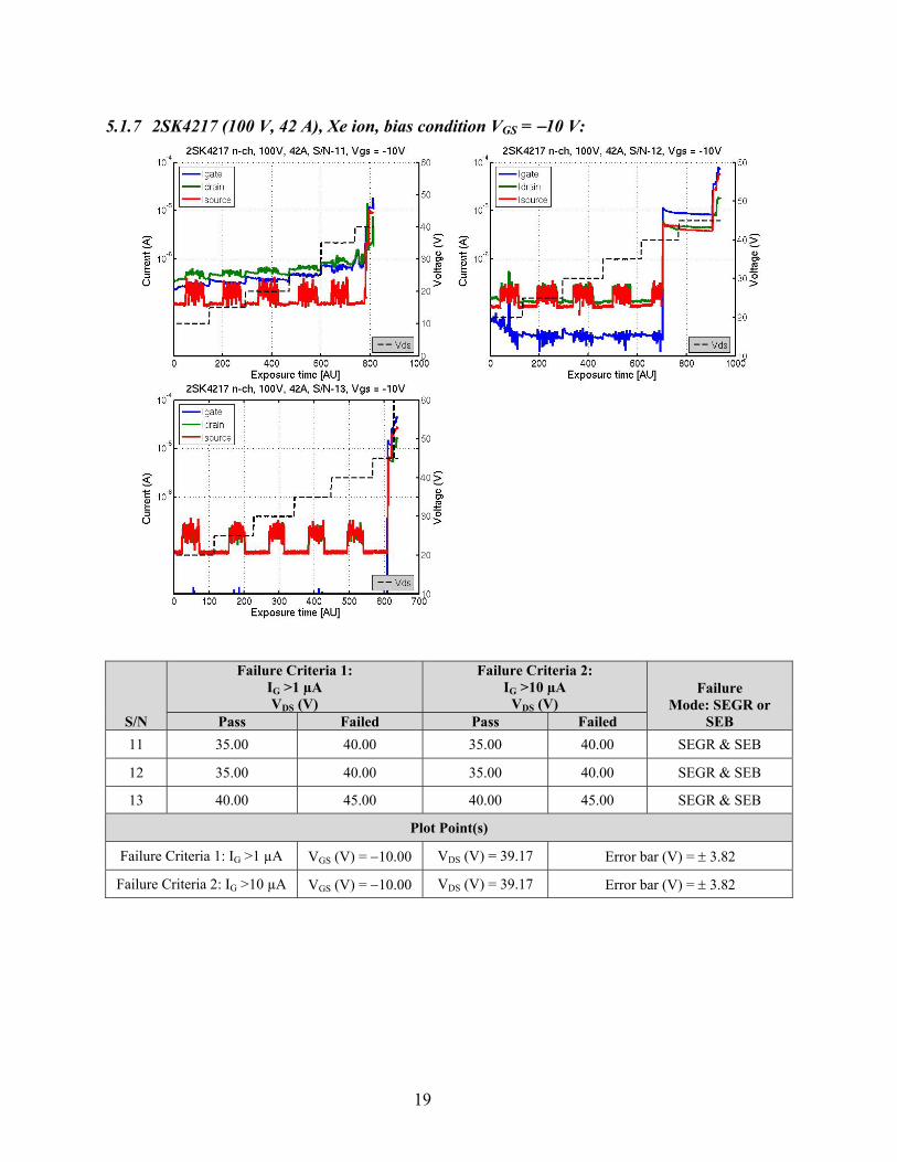
5.1.7 2SK4217 (100 V, 42 A), Xe ion, bias condition VGS = −10 V:
S/N
Failure Criteria 1: IG >1 µA VDS (V)
Failure Criteria 2: IG >10 µA
VDS (V) Failure
Mode: SEGR or SEB Pass Failed Pass Failed
11 35.00 40.00 35.00 40.00 SEGR & SEB
12 35.00 40.00 35.00 40.00 SEGR & SEB
13 40.00 45.00 40.00 45.00 SEGR & SEB
Plot Point(s)
Failure Criteria 1: IG >1 µA VGS (V) = −10.00 VDS (V) = 39.17 Error bar (V) = ± 3.82
Failure Criteria 2: IG >10 µA VGS (V) = −10.00 VDS (V) = 39.17 Error bar (V) = ± 3.82

20
5.1.8 2SK4217 (100 V, 42 A), Xe ion, bias condition VGS = −15 V:
S/N
Failure Criteria 1: IG >1 µA VDS (V)
Failure Criteria 2: IG >10 µA
VDS (V) Failure
Mode: SEGR or SEB Pass Failed Pass Failed
16 25.00 30.00 25.00 30.00 SEGR
17 25.00 30.00 25.00 30.00 SEGR & SEB
18 30.00 35.00 30.00 35.00 SEGR & SEB
Plot Point(s)
Failure Criteria 1: IG >1 µA VGS (V) = −15.00 VDS (V) = 29.17 Error bar (V) = ± 3.82
Failure Criteria 2: IG >10 µA VGS (V) = −15.00 VDS (V) = 29.17 Error bar (V) = ± 3.82
21
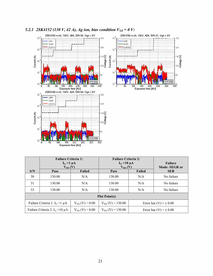
5.2.1 2SK4152 (130 V, 42 A), Ag ion, bias condition VGS = 0 V:
S/N
Failure Criteria 1: IG >1 µA VDS (V)
Failure Criteria 2: IG >10 µA
VDS (V) Failure
Mode: SEGR or SEB Pass Failed Pass Failed
30 130.00 N/A 130.00 N/A No failure
31 130.00 N/A 130.00 N/A No failure
33 130.00 N/A 130.00 N/A No failure
Plot Point(s)
Failure Criteria 1: IG >1 µA VGS (V) = 0.00 VDS (V) = 130.00 Error bar (V) = ± 0.00
Failure Criteria 2: IG >10 µA VGS (V) = 0.00 VDS (V) = 130.00 Error bar (V) = ± 0.00

22
5.2.2 2SK4152 (130 V, 42 A), Ag ion, bias condition VGS = −5 V:
S/N
Failure Criteria 1: IG >1 µA VDS (V)
Failure Criteria 2: IG >10 µA
VDS (V) Failure
Mode: SEGR or SEB Pass Failed Pass Failed
27 65.00 71.50 110.50 117.00 SEGR
28 N/A N/A 123.50 130.00 SEGR
29 N/A N/A 123.50 130.00 SEGR
34 98.00 103.00 121.50 128.00 SEGR
Plot Point(s)
Failure Criteria 1: IG >1 µA VGS (V) = −5.00 VDS (V) = 84.38 Error bar (V) = ± 23.05
Failure Criteria 2: IG >10 µA VGS (V) = −5.00 VDS (V) = 123.00 Error bar (V) = ± 7.04

23
5.2.3 2SK4152 (130 V, 42 A), Ag ion, bias condition VGS = −10 V:
S/N
Failure Criteria 1: IG >1 µA VDS (V)
Failure Criteria 2: IG >10 µA
VDS (V) Failure
Mode: SEGR or SEB Pass Failed Pass Failed
19 45.50 52.00 45.50 52.00 SEGR
23 45.50 52.00 45.50 52.00 SEGR & SEB
25 45.50 52.00 52.00 58.50 SEGR & SEB
Plot Point(s)
Failure Criteria 1: IG >1 µA VGS (V) = −10.00 VDS (V) = 48.75 Error bar (V) = ± 3.25
Failure Criteria 2: IG >10 µA VGS (V) = −10.00 VDS (V) = 50.92 Error bar (V) = ± 4.96

24
5.2.4 2SK4152 (130 V, 42 A), Ag ion, bias condition VGS = −15 V:
S/N
Failure Criteria 1: IG >1 µA VDS (V)
Failure Criteria 2: IG >10 µA
VDS (V) Failure
Mode: SEGR or SEB Pass Failed Pass Failed
15 32.50 39.00 32.50 39.00 SEGR
16 32.50 39.00 32.50 39.00 SEGR & SEB
17 32.50 39.00 32.50 39.00 SEGR
Plot Point(s)
Failure Criteria 1: IG >1 µA VGS (V) = −15.00 VDS (V) = 35.75 Error bar (V) = ± 3.25
Failure Criteria 2: IG >10 µA VGS (V) = −15.00 VDS (V) = 35.75 Error bar (V) = ± 3.25

25
5.2.5 2SK4152 (130 V, 42 A), Xe ion, bias condition VGS = 0 V:
S/N
Failure Criteria 1: IG >1 µA VDS (V)
Failure Criteria 2: IG >10 µA
VDS (V) Failure
Mode: SEGR or SEB Pass Failed Pass Failed
02 65.00 71.50 91.00 97.5 SEGR
03 N/A N/A 6.60 65.00 SEGR
04 65.00 71.50 78.00 84.50 SEGR
Plot Point(s)
Failure Criteria 1: IG >1 µA VGS (V) = 0.00 VDS (V) = 68.25 Error bar (V) = ± 3.25
Failure Criteria 2: IG >10 µA VGS (V) = 0.00 VDS (V) = 70.42 Error bar (V) = ± 30.86

26
5.2.6 2SK4152 (130 V, 42 A), Xe ion, bias condition VGS = −5 V:
S/N
Failure Criteria 1: IG >1 µA VDS (V)
Failure Criteria 2: IG >10 µA
VDS (V) Failure
Mode: SEGR or SEB Pass Failed Pass Failed
05 N/A N/A N/A N/A SEGR
06 N/A N/A N/A N/A SEGR
34 98.00 103.00 123.00 128.00 SEGR
07 52.00 58.50 58.50 65.00 SEGR
Plot Point(s)
Failure Criteria 1: IG >1 µA VGS (V) = −5.00 VDS (V) = 77.50 Error bar (V) = ± 31.63
Failure Criteria 2: IG >10 µA VGS (V) = −5.00 VDS (V) = 93.25 Error bar (V) = ± 22.33

27
5.2.7 2SK4152 (130 V, 42 A), Xe ion, bias condition VGS = −10 V:
S/N
Failure Criteria 1: IG >1 µA VDS (V)
Failure Criteria 2: IG >10 µA
VDS (V) Failure
Mode: SEGR or SEB Pass Failed Pass Failed
08 38.00 45.50 38.00 45.50 SEGR & SEB
10 N/A N/A 38.00 45.50 SEGR & SEB
11 38.00 45.50 38.00 45.50 SEGR & SEB
Plot Point(s)
Failure Criteria 1: IG >1 µA VGS (V) = −5.00 VDS (V) = 41.75 Error bar (V) = ± 3.25
Failure Criteria 2: IG >10 µA VGS (V) = −5.00 VDS (V) = 41.75 Error bar (V) = ± 3.25
28
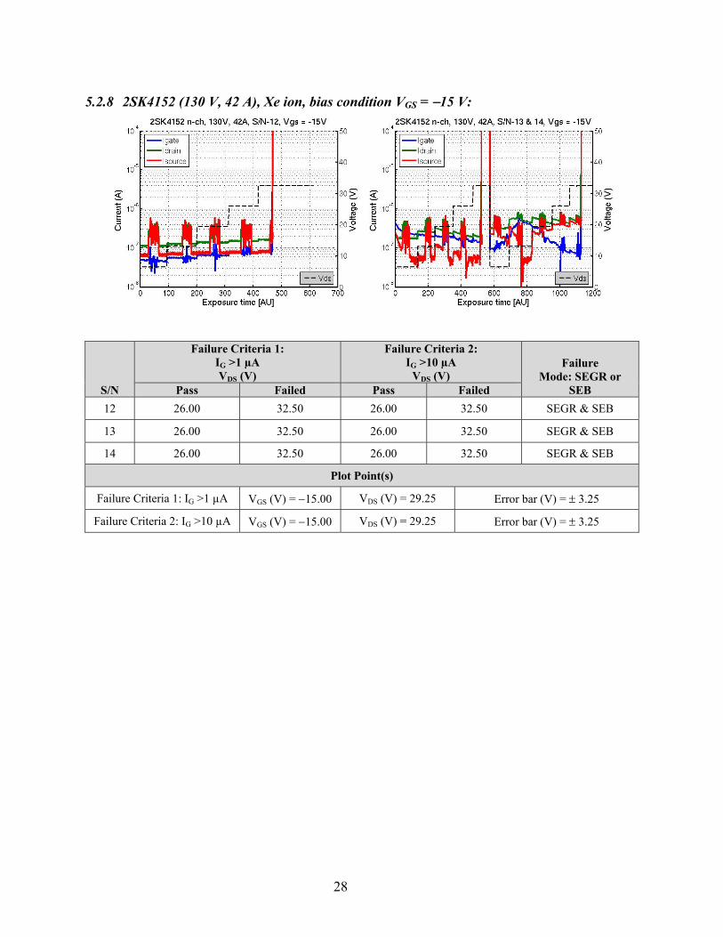
5.2.8 2SK4152 (130 V, 42 A), Xe ion, bias condition VGS = −15 V:
S/N
Failure Criteria 1: IG >1 µA VDS (V)
Failure Criteria 2: IG >10 µA
VDS (V) Failure
Mode: SEGR or SEB Pass Failed Pass Failed
12 26.00 32.50 26.00 32.50 SEGR & SEB
13 26.00 32.50 26.00 32.50 SEGR & SEB
14 26.00 32.50 26.00 32.50 SEGR & SEB
Plot Point(s)
Failure Criteria 1: IG >1 µA VGS (V) = −15.00 VDS (V) = 29.25 Error bar (V) = ± 3.25
Failure Criteria 2: IG >10 µA VGS (V) = −15.00 VDS (V) = 29.25 Error bar (V) = ± 3.25

29
5.3.1 2SK4155 (200 V, 42 A) Ag ion, bias condition VGS = 0 V:
S/N
Failure Criteria 1: IG >1 µA VDS (V)
Failure Criteria 2: IG >10 µA
VDS (V) Failure
Mode: SEGR or SEB Pass Failed Pass Failed
30 200.00 N/A 200.00 N/A No failure
33 200.00 N/A 200.00 N/A No failure
34 200.00 N/A 200.00 N/A No failure
Plot Point(s)
Failure Criteria 1: IG >1 µA VGS (V) = 0.00 VDS (V) = 200.00 Error bar (V) = ± 0.00
Failure Criteria 2: IG >10 µA VGS (V) = 0.00 VDS (V) = 200.00 Error bar (V) = ± 0.00

30
5.3.2 2SK4155 (200 V, 42 A) Ag ion, bias condition VGS = −5 V:
S/N
Failure Criteria 1: IG >1 µA VDS (V)
Failure Criteria 2: IG >10 µA
VDS (V) Failure
Mode: SEGR or SEB Pass Failed Pass Failed
26 60.00 70.00 130.00 140.00 SEGR
28 100.00 110.00 170.00 180.00 SEGR
29 140.00 150.00 180.00 190.00 SEGR
35 N/A 110.00 180.00 190.00 SEGR
Plot Point(s)
Failure Criteria 1: IG >1 µA VGS (V) = −5.00 VDS (V) = 105.00 Error bar (V) = ± 40.31
Failure Criteria 2: IG >10 µA VGS (V) = −5.00 VDS (V) = 170.00 Error bar (V) = ± 24.32

31
5.3.3 2SK4155 (200 V, 42 A) Ag ion, bias condition VGS = −10 V:
S/N
Failure Criteria 1: IG >1 µA VDS (V)
Failure Criteria 2: IG >10 µA
VDS (V) Failure
Mode: SEGR or SEB Pass Failed Pass Failed
22 50.00 60.00 50.00 60.00 SEGR
23 50.00 60.00 50.00 60.00 SEGR
25 50.00 60.00 50.00 60.00 SEGR
Plot Point(s)
Failure Criteria 1: IG >1 µA VGS (V) = −10.00 VDS (V) = 55.00 Error bar (V) = ± 5.00
Failure Criteria 2: IG >10 µA VGS (V) = −10.00 VDS (V) = 55.00 Error bar (V) = ± 5.00

32
5.3.4 2SK4155 (200 V, 42 A) Ag ion, bias condition VGS = −15 V:
S/N
Failure Criteria 1: IG >1 µA VDS (V)
Failure Criteria 2: IG >10 µA
VDS (V) Failure
Mode: SEGR or SEB Pass Failed Pass Failed
18 40.00 50.00 40.00 50.00 SEGR & SEB
19 30.00 40.00 30.00 40.00 SEGR & SEB
20 40.00 50.00 40.00 50.00 SEGR
36 40.00 50.00 40.00 50.00 SEGR
Plot Point(s)
Failure Criteria 1: IG >1 µA VGS (V) = −15.00 VDS (V) = 42.50 Error bar (V) = ± 7.07
Failure Criteria 2: IG >10 µA VGS (V) = −15.00 VDS (V) = 42.50 Error bar (V) = ± 7.07

33
5.3.5 2SK4155 (200 V, 42 A) Xe ion, bias condition VGS = 0 V:
S/N
Failure Criteria 1: IG >1 µA VDS (V)
Failure Criteria 2: IG >10 µA
VDS (V) Failure
Mode: SEGR or SEB Pass Failed Pass Failed
02 70.00 80.00 110.00 120.00 SEGR
03 N/A N/A 100.00 110.00 SEGR
04 80.00 90.00 110.00 120.00 SEGR
Plot Point(s)
Failure Criteria 1: IG >1 µA VGS (V) = 0.00 VDS (V) = 80.00 Error bar (V) = ± 8.66
Failure Criteria 2: IG >10 µA VGS (V) = 0.00 VDS (V) = 111.67 Error bar (V) = ± 7.64

34
5.3.6 2SK4155 (200 V, 42 A) Xe ion, bias condition VGS = −5 V:
S/N
Failure Criteria 1: IG >1 µA VDS (V)
Failure Criteria 2: IG >10 µA
VDS (V) Failure
Mode: SEGR or SEB Pass Failed Pass Failed
05 60.00 70.00 60.00 70.00 SEGR
07 60.00 70.00 60.00 70.00 SEGR
09 50.00 60.00 60.00 70.00 SEGR
Plot Point(s)
Failure Criteria 1: IG >1 µA VGS (V) = −5.00 VDS (V) = 61.67 Error bar (V) = ± 7.64
Failure Criteria 2: IG >10 µA VGS (V) = −5.00 VDS (V) = 65.00 Error bar (V) = ± 5.00

35
5.3.7 2SK4155 (200 V, 42 A) Xe ion, bias condition VGS = −10 V:
S/N
Failure Criteria 1: IG >1 µA VDS (V)
Failure Criteria 2: IG >10 µA
VDS (V) Failure
Mode: SEGR or SEB Pass Failed Pass Failed
10 40.00 50.00 40.00 50.00 SEGR & SEB
11 30.00 40.00 40.00 50.00 SEGR
12 40.00 50.00 40.00 50.00 SEGR
Plot Point(s)
Failure Criteria 1: IG >1 µA VGS (V) = −10.00 VDS (V) = 41.67 Error bar (V) = ± 7.64
Failure Criteria 2: IG >10 µA VGS (V) = −10.00 VDS (V) = 45.00 Error bar (V) = ± 5.00

36
5.3.8 2SK4155 (200 V, 42 A) Xe ion, bias condition VGS = −15 V:
S/N
Failure Criteria 1: IG >1 µA VDS (V)
Failure Criteria 2: IG >10 µA
VDS (V) Failure
Mode: SEGR or SEB Pass Failed Pass Failed
13 30.00 40.00 30.00 40.00 SEGR & SEB
15 30.00 40.00 30.00 40.00 SEGR & SEB
16 30.00 40.00 30.00 40.00 SEGR & SEB
Plot Point(s)
Failure Criteria 1: IG >1 µA VGS (V) = −15.00 VDS (V) = 35.00 Error bar (V) = ± 5.00
Failure Criteria 2: IG >10 µA VGS (V) = −15.00 VDS (V) = 35.00 Error bar (V) = ± 5.00

37
5.4.1 2SK4158 (250 V, 42 A) Ag ion, bias condition VGS = 0 V:
S/N
Failure Criteria 1: IG >1 µA VDS (V)
Failure Criteria 2: IG >10 µA
VDS (V) Failure
Mode: SEGR or SEB Pass Failed Pass Failed
30 250.00 N/A 250.00 N/A No failure
31 250.00 N/A 250.00 N/A No failure
32 250.00 N/A 250.00 N/A No failure
Plot Point(s)
Failure Criteria 1: IG >1 µA VGS (V) = 0.00 VDS (V) = 250.00 Error bar (V) = ± 0.00
Failure Criteria 2: IG >10 µA VGS (V) = 0.00 VDS (V) = 250.00 Error bar (V) = ± 0.00

38
5.4.2 2SK4158 (250 V, 42 A) Ag ion, bias condition VGS = −5 V:
S/N
Failure Criteria 1: IG >1 µA VDS (V)
Failure Criteria 2: IG >10 µA
VDS (V) Failure
Mode: SEGR or SEB Pass Failed Pass Failed
27 100.00 125.00 250.00 N/A SEGR
28 N/A N/A 212.50 225.00 SEGR
29 N/A N/A 250.00 N/A No failure
33 187.50 200.00 250.00 N/A SEGR
Plot Point(s)
Failure Criteria 1: IG >1 µA VGS (V) = −5.00 VDS (V) = 153.13 Error bar (V) = ± 57.79
Failure Criteria 2: IG >10 µA VGS (V) = −5.00 VDS (V) = 242.19 Error bar (V) = ± 16.83

39
5.4.3 2SK4158 (250 V, 42 A) Ag ion, bias condition VGS = −10 V:
S/N
Failure Criteria 1: IG >1 µA VDS (V)
Failure Criteria 2: IG >10 µA
VDS (V) Failure
Mode: SEGR or SEB Pass Failed Pass Failed
21 50.00 62.50 50.00 62.50 SEGR
25 50.00 62.50 50.00 62.50 SEGR
26 50.00 62.50 50.00 62.50 SEGR
Plot Point(s)
Failure Criteria 1: IG >1 µA VGS (V) = −10.00 VDS (V) = 56.25 Error bar (V) = ± 6.25
Failure Criteria 2: IG >10 µA VGS (V) = −10.00 VDS (V) = 56.25 Error bar (V) = ± 6.25

40
5.4.4 2SK4158 (250 V, 42 A) Ag ion, bias condition VGS = −15 V:
S/N
Failure Criteria 1: IG >1 µA VDS (V)
Failure Criteria 2: IG >10 µA
VDS (V) Failure
Mode: SEGR or SEB Pass Failed Pass Failed
18 38.50 50.00 38.50 50.00 SEGR & SEB
19 38.50 50.00 38.50 50.00 SEGR & SEB
20 42.50 55.00 42.50 55.00 SEGR & SEB
Plot Point(s)
Failure Criteria 1: IG >1 µA VGS (V) = −15.00 VDS (V) = 45.75 Error bar (V) = ± 6.77
Failure Criteria 2: IG >10 µA VGS (V) = −15.00 VDS (V) = 45.75 Error bar (V) = ± 6.77

41
5.4.5 2SK4158 (250 V, 42 A) Xe ion, bias condition VGS = 0 V:
S/N
Failure Criteria 1: IG >1 µA VDS (V)
Failure Criteria 2: IG >10 µA
VDS (V) Failure
Mode: SEGR or SEB Pass Failed Pass Failed
02 75.00 87.50 100.00 112.50 SEGR
03 N/A N/A 137.50 150.00 SEGR
05 75.00 87.50 87.50 100.00 SEGR
Plot Point(s)
Failure Criteria 1: IG >1 µA VGS (V) = 0.00 VDS (V) = 81.25 Error bar (V) = ± 6.25
Failure Criteria 2: IG >10 µA VGS (V) = 0.00 VDS (V) = 114.58 Error bar (V) = ± 26.76

42
5.4.6 2SK4158 (250 V, 42 A) Xe ion, bias condition VGS = −5 V:
S/N
Failure Criteria 1: IG >1 µA VDS (V)
Failure Criteria 2: IG >10 µA
VDS (V) Failure
Mode: SEGR or SEB Pass Failed Pass Failed
06 50.00 62.50 62.50 75.00 SEGR
07 50.00 62.50 62.50 75.00 SEGR
09 50.00 62.50 62.50 75.00 SEGR
Plot Point(s)
Failure Criteria 1: IG >1 µA VGS (V) = −5.00 VDS (V) = 56.25 Error bar (V) = ± 6.25
Failure Criteria 2: IG >10 µA VGS (V) = −5.00 VDS (V) = 68.75 Error bar (V) = ± 6.25

43
5.4.7 2SK4158 (250 V, 42 A) Xe ion, bias condition VGS = −10 V:
S/N
Failure Criteria 1: IG >1 µA VDS (V)
Failure Criteria 2: IG >10 µA
VDS (V) Failure
Mode: SEGR or SEB Pass Failed Pass Failed
10 37.50 50.00 37.50 50.00 SEGR
12 37.50 50.00 37.50 50.00 SEGR
13 37.50 50.00 37.50 50.00 SEGR
Plot Point(s)
Failure Criteria 1: IG >1 µA VGS (V) = −10.00 VDS (V) = 43.75 Error bar (V) = ± 6.25
Failure Criteria 2: IG >10 µA VGS (V) = −10.00 VDS (V) = 43.75 Error bar (V) = ± 6.25

44
5.4.8 2SK4158 (250 V, 42 A) Xe ion, bias condition VGS = −15 V:
S/N
Failure Criteria 1: IG >1 µA VDS (V)
Failure Criteria 2: IG >10 µA
VDS (V) Failure
Mode: SEGR or SEB Pass Failed Pass Failed
14 37.50 50.00 37.50 50.00 SEGR
15 37.50 50.00 37.50 50.00 SEGR & SEB
16 25.00 37.50 25.00 37.50 SEGR
Plot Point(s)
Failure Criteria 1: IG >1 µA VGS (V) = −15.00 VDS (V) = 39.58 Error bar (V) = ± 9.55
Failure Criteria 2: IG >10 µA VGS (V) = −15.00 VDS (V) = 39.58 Error bar (V) = ± 9.55
45
6. References [1] D. K. Nichols, K. P. McCarty, J. R. Coss, A. Waskiewicz, J. Groninger, D. Oberg, J.
Wert, P. Wajewski, and R. Koga, “Observations of Single Event Failure in Power MOSFETs,” IEEE Radiation Effects Data Workshop, p. 41, Dec. 1994.
[2] D. K. Nichols, J. R. Coss, T. Miyahira, J. Titus, D. Oberg, J. West, P. Wajewski, and J. Lintz, “Update of Single Event Failure in Power MOSFETs,” IEEE Radiation Effects Data Workshop, p. 67, Dec. 1996.
[3] J. R. Coss, G. M. Swift, L. E. Selva, J. L. Titus, E. Normand, D. L. Oberg, and J. L. West, “Compendium of Single Event Failures in Power MOSFETs,” IEEE Radiation Effects Data Workshop, p. 15, Dec. 1997.
[4] eeepitnl.tksc.jaxa.jp/JP/event/MEWS/21th/data/2-2.pdf.
[5] JAXA. “SEE Test Results of Fuji Power MOSFETs,” Jan. 2008.
[6] L. Scheick, “Testing Guideline for Single Event Gate Rupture (SEGR) of Power MOSFETs,” http://parts.jpl.nasa.gov/docs/NEPP07/NEPP07TestingSEGRMOSFETs.pdf, Feb. 2008.
[7] L. E. Selva, L. Z. Scheick, S. McClure, T. Miyahira, S. M. Guertin, S. K. Shah, L. D. Edmonds, and J. D. Patterson, “Catastrophic SEE in High-Voltage Power MOSFETs,” IEEE Radiation Effects Data Workshop, p. 113, Dec. 2003.
[8] L. Scheick, and L. Selva, “Effect of Dose History on SEGR Properties of Power MOSFETs,” IEEE TNS 54(6): 2568, Dec. 2007.
Related Documents