S3FN429 Sensorless Control of BLDC motor Revision 1.00 May 2012 A A p p p p l l i i c c a a t t i i o o n n N N o o t t e e 2011 Samsung Electronics Co., Ltd. All rights reserved.

Welcome message from author
This document is posted to help you gain knowledge. Please leave a comment to let me know what you think about it! Share it to your friends and learn new things together.
Transcript

S3FN429
Sensorless Control of BLDC motor
Revision 1.00
May 2012
AApppplliiccaattiioonn NNoottee
2011 Samsung Electronics Co., Ltd. All rights reserved.

Important Notice
The information in this publication has been carefully checked and is believed to be entirely accurate at the time of publication. Samsung assumes no responsibility, however, for possible errors or omissions, or for any consequences resulting from the use of the information contained herein.
Samsung reserves the right to make changes in its products or product specifications with the intent to improve function or design at any time and without notice and is not required to update this documentation to reflect such changes.
This publication does not convey to a purchaser of semiconductor devices described herein any license under the patent rights of Samsung or others.
Samsung makes no warranty, representation, or guarantee regarding the suitability of its products for any particular purpose, nor does Samsung assume any liability arising out of the application or use of any product or circuit and specifically disclaims any and all liability, including without limitation any consequential or incidental damages.
"Typical" parameters can and do vary in different applications. All operating parameters, including "Typicals" must be validated for each customer application by the customer's technical experts.
Samsung products are not designed, intended, or authorized for use as components in systems intended for surgical implant into the body, for other applications intended to support or sustain life, or for any other application in which the failure of the Samsung product could create a situation where personal injury or death may occur.
Should the Buyer purchase or use a Samsung product for any such unintended or unauthorized application, the Buyer shall indemnify and hold Samsung and its officers, employees, subsidiaries, affiliates, and distributors harmless against all claims, costs, damages, expenses, and reasonable attorney fees arising out of, either directly or indirectly, any claim of personal injury or death that may be associated with such unintended or unauthorized use, even if such claim alleges that Samsung was negligent regarding the design or manufacture of said product.
Copyright 2011 Samsung Electronics Co., Ltd.
All rights reserved. No part of this publication may be reproduced, stored in a retrieval system, or transmitted in any form or by any means, electric or mechanical, by photocopying, recording, or otherwise, without the prior written consent of Samsung Electronics.
Samsung Electronics Co., Ltd. San #24 Nongseo-Dong, Giheung-Gu Yongin-City, Gyeonggi-Do, Korea 446-711
Contact Us: [email protected] TEL: (82)-(31)-209-4956 FAX: (82)-(31)-209-6494
Home Page: http://www.samsungsemi.com

Revision History
Revision No. Date Description Author(s)
V1.0 2011 11/08 Creation Woncheol Lee
V1.1 2012 6/13 Modification & addition monitor program Woncheol Lee
Youngseob Choi

List of Terms
Terms Descriptions

List of Acronyms
Acronyms Descriptions

S3FM02G429_AN_REV 1.00 1 BLDC MOTOR CONTROL WITH S3FN429
1-1
1 BLDC motor control with S3FN429
1.1 Introduction
This document describes the reference design of a speed control for 3-phase brushless DC (BLDC) motor using S3FN429. The S3FN429 has been developed by Samsung Electronics to 3-phase BLDC motor drives, which is used for the industrial or the appliance. The S3FN429 based on ARM Cortex-M0 core designed specifically for BLDC motor control application. It is well-suited for BLDC motor control offering many dedicated peripherals, such as 4 comparators, PPD(Pulse Position Decoder), 12bit ADC, 3 timers, communications peripherals( USART,SPI), on-board flash and RAM.
BLDC motors are very popular in many applications. In BLDC motors, rotor magnets generate the rotor’s magnetic flux, allowing BLDC motors to achieve higher efficiency. Therefore, BLDC motors may be used in high-end appliances (refrigerators, washing machines, dishwashers, etc.), high-end pumps, fans, and other appliances that require high reliability and efficiency.
The concept of this application note is to create a speed control of BLDC driver without hall sensors. It serves as an example of a BLDC motor control system design using a Samsung microprocessor S3FN429.
1.2 S3FN429 Microprocessor
The S3FN429 MCU is provided in a 44-pin QFP package and has 32 KBytes of flash, 2 KBytes RAM, IMC(Inverter Motor Controller : PWM generation for 3-phase motor ), PPD(Pulse Position Decoder), comparators, operational amplifier and 12-bit AD converters. This 32-bit device is based on the ARM Cortex-M0 architecture operating at a core frequency up to 40 MHz. On-chip modules include:
Built-in up to 32 Kbytes Program Flash Memory
Internal up to 2 Kbytes SRAM for stack, data memory, or code memory
32 General Purpose I/Os (GPIO)
Operating temperature: –40 ~ 105C
Operating voltage range: 2.5 ~ 5.5V
Interrupt controller: Dynamically reconfigurable Nested Vectored Interrupt Controller (NVIC)
Clock and Power Management Controller (CM)
Watch-Dog Timer (WDT)
3 16-bit Timer/Counters (TC)
4 16-bit PWM
1 16-bit Pulse Position Decoder (PPD)
1 3-Phase Inverter Motor Controller (IMC)
1 USART, 1 SPI
12-bit ADC with external input AINx 10ch
1 OP-AMP

S3FM02G429_AN_REV 1.00 1 BLDC MOTOR CONTROL WITH S3FN429
1-2
4 Comparator
Support Idle and Stop mode for reducing current
1.3 BLDC motor theory
Brushless Direct Current motors, known that as DC motors, are used for many industrial applications. It is generally composed of two parts: a rotor made up of permanent magnets and a stator with windings and slots. In figure.1-1, there are 4 permanent magnets as the rotor and 6 slots as the stator. The combination of 3 phase stator and permanent magnet rotor is most popular in the industrial. The pole pair of rotor has various numbers for each application.
In recent years, the developments of μ-processor and electric power switches have provided innovations of motor drive systems. Especially the mechanical commutator and brushes in the DC motors have been eliminated in BLDC motor with retaining many useful properties. In oder to replace the mechanical commutator, therefore, electronic commutator is adopted to generate sequential switching patterns for commutation. So, this is why it is called a BLDC(Brushless DC) motor. A BLDC motor has many merits over DC motors. Therefore, rotor speed of BLDC motor is not affected by the stress limitation of brushes. Because it has no brushes and mechanical commutator to generate the sparks, it can be used in harsh conditions. It is more efficient, reliable and generally lower maintenance than DC motors.
Figure.1-1 shows the cross section of a 3-phase BLDC motor. But the BLDC motors have some limitations for proper operation. Rotor position information must be required for BLDC drive operation, so hall-effect sensors or the back EMF zero-crossing information equivalent to hall signals must be used to obtain this information. Generally, incorrect control of a BLDC motor, especially at high temperatures, can damage its permanent magnet, so careful design of the control scheme is essential.
Figure 1-1 The cross section of a 2 pole pair 3 phase BLDC motor
As you can see figure.1-2, the BLDC drive system consists of inverter and controller with 3-phase BLDC motor. The motor is fed from a three-phase inverter. In this figure, the rotor positions represent three hall-effect sensors mounted in or near the machine’s air gap to detect the position of the rotor magnets. These sensors are located 120 degrees apart around the stator. Depending on which magnetic field passes over each sensor, the output may be high or low. Thus hall-effect sensors provide information about polarity and position. The electric commutaton sequences can be simply triggered by the use of signals from these sensors. So these are composed six switching vectors to generate output voltages for proper rotation of BLDC. The inverter in figure.1-2 is consists of 6 power switches (MOSFET or IGBT). It is a 3-phase full bridge circuit inverter that is a power conversion

S3FM02G429_AN_REV 1.00 1 BLDC MOTOR CONTROL WITH S3FN429
1-3
device converting from DC input power to 3 phase AC power. In this figure, the interface circuit is gate drive circuit for 3-phase inverter.
Table 1-1 shows the six vector commutation for 120-degree modulation based on hall-effect sensors state. The vectors are 3 digit binary numbers, the level of hall-effect sensor on the U-phase is the MSB and the one of W-phase is LSB. For the control of electric commutation for BLDC, MCU reads the states on the three hall-effect sensors, then it calculates the vectors in every control periods. As a result, it assigns the output port for electric power switching to generate output voltages. Fig. 3 shows the six-vector sequence for BLDC motor. For CW(Clock Wise) rotation, the vectors are executed in order as 5 4 6 2 3 1 6.
Figure 1-2 BLDC drive system with a inverter and hall sensors
Table 1-1 Six vectors for 120-degree modulation
Vector U_hall V-phase W-phase Remark
4 1 0 1 U_high
V_low
6 1 0 0 U_high
W_low
2 1 1 0 V_high
W_low
3 0 1 0 V_high
U_low
1 0 1 1 W_high
U_low
5 0 0 1 W_high
V_low
BLDC motor generally has a rectangular air-gap flux density and produces a trapezoidal back-EMF in the stator. Back-EMF waveforms(eu,ev,ew) for an ideal case are shown in Fig. 4. The current waveforms(iu,iv,iw) are also shown in this figure. Therefore the BLDC motor generates constant torque when excited with six-vector switched current waveforms, as shown in this figure. The BLDC motor maintains high efficiency across wide speed range. Because BLDC motor maintains higher efficiency compared to induction motor, so it is valid solution to variable speed drive application. Also Fig.4 shows that two of the phases have back EMF waveforms that are flat during
S3FM02G429_AN_REV 1.00 1 BLDC MOTOR CONTROL WITH S3FN429
1-4
every 60-degree interval. In the operation of a BLDC motor, during each of these 60-degree intervals, the two phases with the flat EMF waveforms are effectively connected in series and the current through them is controlled, while the third phase is open state.
Figure 1-3 Six vector sequence modulation for BLDC clock wise rotation
Figure 1-4 Induced EMF and phase current in 3-phase BLDC

S3FM02G429_AN_REV 1.00 1 BLDC MOTOR CONTROL WITH S3FN429
1-5
1.4 Sensorless Control of BLDC
In case of BLDC drive system utilizing hall sensors, hall sensor circuit and control are simple but these will increase the cost and the size of the motor. In some applications like as a compressor application for air-conditioner, it may not be acceptable to mount any hall sensors on the stator. Therefore, BLDC sensorless control has been receiving great interest in recent years. Typically, BLDC motors are fed by a three-phase inverter with, what is called, electric commutation. The commutation interval for each step is 60 degrees by electrical angle. It is determined by the rotor position, which can be detected by estimated hall signals from the back EMF zero-crossing. Of course, there are many other sensorless techniques, these techniques require more complex calculation than the back EMF method, so there are some limitation in the applications.
As mentioned before, three-phase BLDC motor is driven with six-step 120 degree control method. That means the conduction interval of one phase is 120 degree. Therefore, the Back-EMF zero-crossing detecting technique is based on the fact that only two phases of a BLDC motor are connected to the power source at one time instant so the third phase can be used to detect zero-crossing of the Back-EMF voltage. For example, when phase U and phase V are connected to the source, phase W is floating. No current is going through this phase. This conducting interval lasts 60 electrical degrees, which is called commutation step. This is described by the following conditions:
If U phase High, V phase Low,
V V , V GND
IU IV IW 0
The terminal voltage of floating phase W can be calculated when considering the above conditions:
WV3
2eW
VDC
2
U3
2eU
V
2
V3
2eU
V
2
In these equations, forward voltage drop of MOSFET and body diode is ignored for simplification. So if you compare terminal voltages(VU,VV,VW) with a reference voltage by using 3 comparators, then you can detect the zero-crossing point of back EMF voltages. But the terminal voltages contain many harmonic components with several times of PWM switching frequency. So the Low Pass Filter(LPF) circuit are used to eliminate the harmonic components. And then you can detect the zero-crossing point with internal comparators. When a zero crossing is detected, several calculations start. The next commutation time is calculated by computations of the actual speed. The speed command is set according to the state of the run/stop state and the target speed from user.
1.5 Speed Control of BLDC
The applied voltage and back-EMF are balanced so that the torque necessary to maintain rotor speed is achieved. Torque from BLDC motors is proportional to the current passing through the stator windings. Therefore, to increase the speed, we must increase the current. As a result, torque is maintained at the load torque level by changing the current to maintain the desired speed. So in order to change the motor speed, the current can be controllable. It is difficult to adjust current directly. However, current indirectly can be adjusted by regulating the voltage. Applied voltage to BLDC motor is regulated using the pulse width modulation (PWM) method. In other

S3FM02G429_AN_REV 1.00 1 BLDC MOTOR CONTROL WITH S3FN429
1-6
words, the amplitude of the applied voltage is adjusted by inverter with the PWM technique. During a arbitrary vector, the voltage is turned on and off at a suitable frequency in a manner that applies proper current to each windings. As a result, by adjusting voltage in stator windings, indirectly we can control BLDC motor speed. In this application, a 16 bit PWM timer is used to generate PWM output state.
As mentioned before, electrical commutation ensures the rotor position of the BLDC motor, while the motor speed only depends on the amplitude of the applied voltage from inverter. As shown in Fig.5, the target speed is controlled by a speed controller, which is implemented as a conventional PI(Proportional-Integral) algorithm. The difference between the real and target speeds are inputs to the speed controller which then controls the duty cycle of the PWM which correspond to the voltage amplitude required to maintain the target speed.
Figure 1-5 Speed Controller
Calculated hall signals from back EMF of the 3 phase BLDC motor are supplied into internal comparators to generate 6-multiplied signal by utilizing EX-OR. The 6-multiplied signal is connected to the input of PPD for speed calculation. Two of hall signals can be used to determine the direction of rotation.
The commutation sequence provides the voltage vector of inverter according to rotor position. As mentioned before, there are 6 vectors determined by the level of the 3-calculated hall signals. In the GPIO of the S3FN429, the commutation sequence is determined with level of the 3-calculated hall signals. From this rotor position the voltage vector of inverter is calculated according to required speed. Then appropriate commutation sequence is called. The PWM switching scheme is in the commutation table. Then the commutation is repeated per each 60 electrical degrees.
The PI controller is used for the speed closed loop. The controller is called every 3ms. Real and target speed are inputs to the controller. Output of the controller sets the level of voltage applied to the BLDC motor. The PI gains were tuned experimentally. Because the speed update depends on real motor speed, the gains of speed controller have to be changed according to the maximum measured speed, to achieve the best result.

S3FM02G429_AN_REV 1.00 2 H/W IMPLEMENTATION
2-7
2 H/W Implementation
2.1 System Overview
The motor drive system is designed for a 3-phase BLDC motor. The application meets the following performance
specifications:
• Speed control of a BLDC motor using Hall sensors
• Targeted at S3FN429 BLDC drive board with Oriental BLDC motor
• Control technique incorporates:
— PWM control of BLDC motor with speed-closed loop
— Maximum speed of 4500 RPM
• Manual interface (Start/Stop switch, Up/Down push button control, LED indication)
2.2 Overview of Hardware Implementation
This BLDC demo kit is small single board computer system (Demo kit) designed for S3FN429 MCU of the SAMSUNG electronics based on 32bit ARM Cortex-M0 core.
Table 2- 1 Specification of BLDC demo kit
Item Feature Remarks
1.CPU S3FN429 Operating frequency 40MHz
2.ROM Internal Flash 32KB Program and Constant data store
3.RAM Internal SRAM 2KB Program, stack, user data store
4.Program Download/Execute
JTAG emulator U-Link, SM-Link, J-Link
5. I/O
1. CPU connector for user programming (1) JTAG interface 20 pin connector(J2) 2. Basic I/O (1) 2 key input button(PB1,PB2)
(2) 4 LED output(LED0~LED3)
(3) RS-232C UART connector(P1) 3. additional I/O (1) Voltage input using variable resister(VR1) (2) 14 Test pins TP1~TP14 (3) Motor connection(J1)
For JTAG emulation Standard 9pin RS-232C D-sub PWM output and hall signal input
6. Input Voltage 24V_DC( 5V/15V regulation on the board)
7. PCB 150X150 mm 4-layer Epoxy PCB

S3FM02G429_AN_REV 1.00 2 H/W IMPLEMENTATION
2-8
The basic structure of BLDC demo set is shown in figure 2-1, and then its specifications are shown in table 2-1. The 24V DC input voltage is fully supplied into the board through input power fuse. It is also filtered by the DC-link capacitor. The Mitsubishi IPM(Intelligence Power Module) is implemented to drive BLDC motor. The internal peripheral IMC(Inverter Motor Control1) supplies the PWM pulses for IPM. The current for limitation over current control is sensed with the shunt register(RTS1) located at lower side of IPM. Terminal voltage sensing circuits for zero crossing of back EMF detection are only used for comparator input signals. The SCI is activated for RS-232 communication used for PC monitoring. Using the GPIO, input state selection and output state with LED is used for monitoring.
Figure 2- 1 BLDC Motor Drive System Block
2.3 MCU and supporting circuit
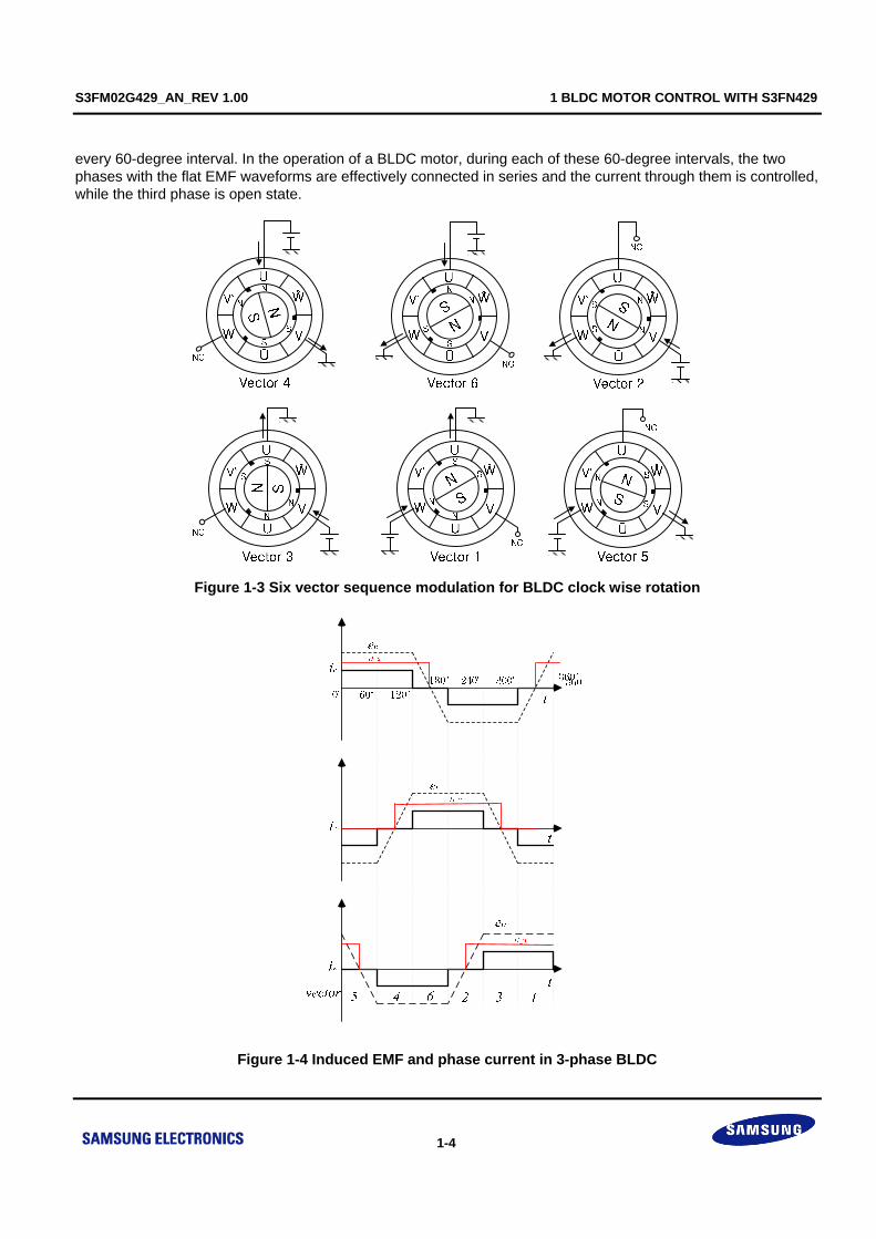
As shown in figure 2-2, MCU device(S3FN429) and its supporting circuits are composed of reset circuit, system clock generation circuit, JTAG interface circuit. MCU device is 44-pin QFP package, system reset circuit is forcibly to reset the system. The circuit is composed R7(10kΩ) and C5(0.01uF) with a push button. The reset signal(nReset) is connected to MCU device or JTAG interface, you can also reset the system through the JTAG emulator. S3FN429 can use 4~12MHz crystal oscillator as a external main clock, 8MHz crystal was implemented in the demo system. The system clock is the 40MHz by using internal PLL block. Capacitors(22pF) are connected to clock generation circuit for stable oscillation. JTAG connector has two connector type(20 pin or 14 pin) in the ARM standard, 20-pin box type connector(J2) is implemented in this demo set. Writing and execution of program and debugging was performed by using KEIL ULINK-Pro.
S3FM02G429_AN_REV 1.00 2 H/W IMPLEMENTATION
2-9
Figure 2- 2 MCU and conditioning circuits
2.4 Intelligent Power Module Connection Circuit
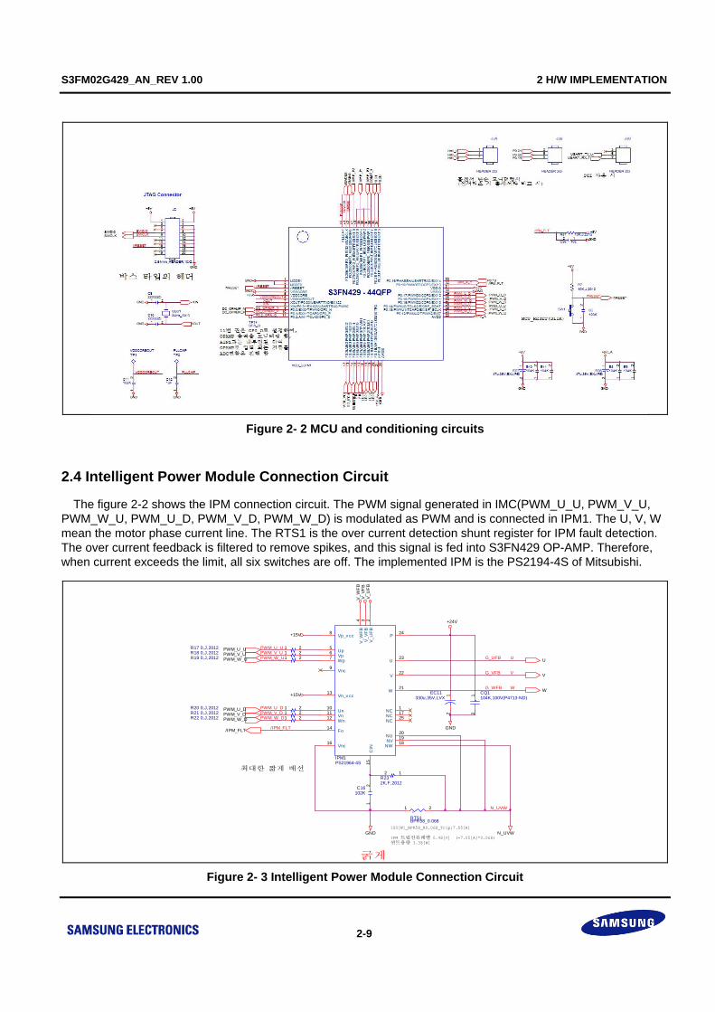
The figure 2-2 shows the IPM connection circuit. The PWM signal generated in IMC(PWM_U_U, PWM_V_U, PWM_W_U, PWM_U_D, PWM_V_D, PWM_W_D) is modulated as PWM and is connected in IPM1. The U, V, W mean the motor phase current line. The RTS1 is the over current detection shunt register for IPM fault detection. The over current feedback is filtered to remove spikes, and this signal is fed into S3FN429 OP-AMP. Therefore, when current exceeds the limit, all six switches are off. The implemented IPM is the PS2194-4S of Mitsubishi.
Figure 2- 3 Intelligent Power Module Connection Circuit
G_WFB
/IPM_FLT
+15V
R20 0,J,2012 1 2
IPM 트립전류레벨 0.48[V] (=7.05[A]*0.068)션트용량 3.38[W]
최대한 짧게 배선
U
N_UVW100[W]_BPR58_R0.068_Trip:7.05[A]
*
RTS1BPR58_0.068
1 2
G_UFB
W
굵게
PWM_W_D
G_VFB
GND
V
CQ1104K,100V(P4713-ND)
12
GND
+15V
R18 0,J,2012 1 2
PWM_V_D
R17 0,J,2012 1 2
+24V
/IPM_FLT
PWM_U_D
PWM_W_D
V_
WF
B
R22 0,J,2012 1 2PWM_V_D
V_
UF
B
IPM1PS21964-4S
1
234
567
8
9
101112
13
14
15
16
17
181920
21
22
23
24
25
NC
V_
UF
BV
_V
FB
V_
WF
B
UpVpWp
Vp_v cc
Vnc
UnVnWn
Vn_v cc
Fo
CINVnc
NC
NWNVNU
W
V
U
P
NC
R21 0,J,2012 1 2PWM_U_D
PWM_W_U
R232K,F,2012
12
V_
VF
B
PWM_W_UR19 0,J,2012 1 2
EC11330u,35V,LVX
12
V
PWM_V_UPWM_V_U
PWM_U_U
U
N_UVW
C16102K
12
PWM_U_U
W

S3FM02G429_AN_REV 1.00 2 H/W IMPLEMENTATION
2-10
2.5 +5[V] and +15[V] Power Source
The 3-phase BLDC Motor Control Drive contains devices that require various voltage levels of +5[V] or +15[V]. The input voltage can be supplied from input connector(CN1).There are no protection for reverse polarity, so the user have to be careful for input voltage polarity. The +5[V] level is generated by means of the MC33063A switching step down regulator, which generates 5 V level from input 24[V] DC. This step down converter can supply up to 1A. This voltage level serves the S3FN429, hall sensors and RS3232 for SCI. If the 5 V level step down converter operates properly, the LED5 red LED is turned on
Also the +15[V] source is necessary to establish the power sources of IPM. The figure 2-6 shows the step down converter that the output are 5[V] and 15[V].
Figure 2- 4 Power Circuit
2.6 RS-232 Circuit for PC Monitoring
The board contains a SCI interface. The main part of the interface is SCI controller RS3232. The figure 2-4 shows the monitoring circuit utilizing the RS-232 communication standard. The USART1_TX_1 , USART1_RX_1 are the transferred and received signal from MCU.
Figure 2- 5 RS-232 Circuit
R41.2K,F,2012
1 2
+5V_A
L2DSC-7850U-221M
1 2
+24V
+5V
U1
MC33063A/SO
5
3
6
87
12COMP
TCAP
VCC
DCPK
SWCSWE
GND
+5V
R53.6K,F,20121 2
+5V
B4104K
12
GND
C3NON
1 2
+24V_RES
R60.5ohm,R51, 6432
1 2
GND
R27.5K,F,20121 2
GND
EC247u,35V,BXJ,F60
12
C4 102K12
GND
L3ILS-1206 10uH1 2
L1DSC-7850U-221M
1 2
GND
GND
C2 102K12
R30.5ohm,R51, 6432
1 2
+15V
SD2KDR400S
23
EC147u,35V,BXJ,F60
12
GND
B2104K
12
U2
MC33063A/SO
5
3
6
87
12COMP
TCAP
VCC
DCPK
SWCSWE
VCC
SD1KDR400S
23
GND
+EC4
220uF,16V,LXV
EC547u,35V,BXJ,F60
12
+15V
C1NON
1 2
B1104K
12
GND
+24V_RES
R1680,F,20121 2
B5104K
12
+24V_RES
+24V_RES
USART_TX_1
+5VP1
9p_dsub/FEMALE/R-angle
594837261
USART_RX_1
B15 1041 2
GND
USART_TX_1
GND
+5V U4
3232_16pin
1
2 3
4
5
6
789
10
1112 13
14
15
16C1+
V+ C1-
C2+
C2-
V-
T2outR2inR2out
T2in
T1inR1out R1in
T1out
GND
VCC
B17 1041 2
GND
B16 1041 2
B19104K
12
USART_RX_1
B18 1041 2

S3FM02G429_AN_REV 1.00 2 H/W IMPLEMENTATION
2-11
2.7 Manual Interface
The figure 2-5 shows the user interface circuit with utilizing the internal peripheral GPIO, NRESET. Three on-board push button switches(MCU_RESET,PB1,PB2) and one toggle switch are provided for the user interface. Two push-button(PB1, PB2) are directly connected to the GPIO. One push-button(MCU_RESET)is provided for nRESET input pin to logic level low. A toggle switch has 2 states(RUN/STOP) to supply/stop power into the motor
Figure 2-6 Key input, LED output Circuits
2.8 Back EMF Voltage Detection Circuit
The figure 2-7 shows the back EMF voltage detection circuit. The switching noises are filtered by RC filters, for example for U-phase, the RC filter was composed R38(240kΩ),R41(27kΩ) with C23(220nF). The SENLESS HALLU, The SENLESS HALLV, The SENLESS HALLW signals should be the input signal of internal peripheral comparator in the MCU. This calculated hall signals only are used for speed control.
Figure 2-7 Back EMF Detection Circuit
GND
R27470, J, 2012
RUN/STOP
GND
R30470, J, 2012
PB1
SW3
+5V
MCU_RESET(SLIK)
R2610K,J,2012
R2410K,J,2012
GND
SW4
LED2LED-GREEN
12
GND
+5V
C19103
12
R2510K,J,2012
GND
nRESET
C5103K
12
R28470, J, 2012
+5V
R29470, J, 2012
GND
+5V
LED3
GND
LED3LED-GREEN
12
LED1
SW1C17103
12
PB1(SLIK)
LED4LED-GREEN
12
nRESET
LED2
RUN/STOP(SLIK)
LED5LED-RED
12
LED0
PB2(SLIK)
SW2AT1D-2M3
1
2
3
LED1LED-GREEN
12
+5V
5[V](SLIK)
C18103
12
R710K,J,2012
GND
GND
R31330,J,3216
12
PB2
GND
U
R4147K,F,3216 1
2
R38240K,F,3216 1
2U
SENLESS_HALL_U SENLESS_HALL_V SENLESS_HALL_W
+5V_A
GND
D6KDR731S
21
3
GND
COMP_N
TP13
DC
_LIN
K_H
ALF
C22102
12
24[V] -> 4[V]
TP6
SE
NLE
SS
_H
ALL
_U +5V_A
GND
D7KDR731S
21
3
GND
C23220n
12
SENLESS_HALL_U
TP7
SE
NL
ES
S_
HA
LL_
V
+5V_A
GND
D8KDR731S
21
3
GND
C25220n
12
SENLESS_HALL_V
+5V_A
GND
D9KDR731S
21
3
GND
C24220n
12
SENLESS_HALL_W
TP8
SE
NLE
SS
_HA
LL_
W
R44510K,F,3216
12
R45510K,F,3216
12
GND
R39240K,F,3216 1
2
R4247K,F,3216 1
2W
R46510K,F,3216
12
GND
V
R4347K,F,3216 1
2
R37240K,F,3216 1
2V
S3FM02G429_AN_REV 1.00 3 SOFTWARE IMPLEMENTATION
3-12
3 Software Implementation
3.1 Software Overview
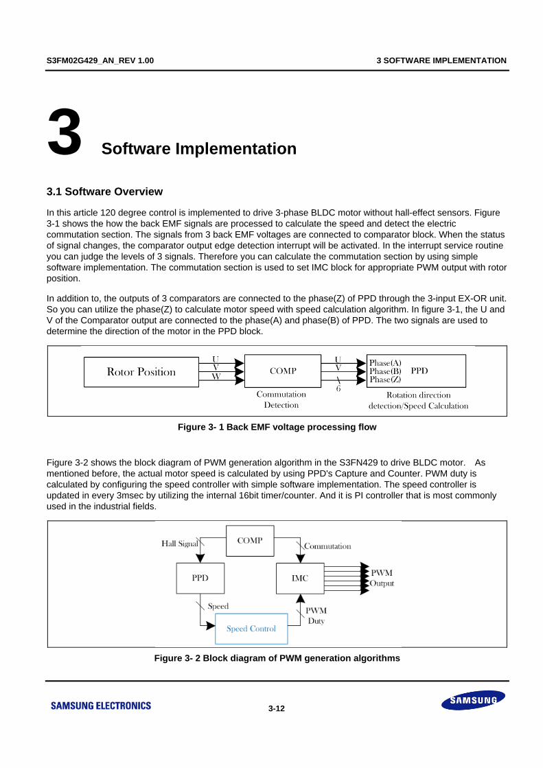
In this article 120 degree control is implemented to drive 3-phase BLDC motor without hall-effect sensors. Figure 3-1 shows the how the back EMF signals are processed to calculate the speed and detect the electric commutation section. The signals from 3 back EMF voltages are connected to comparator block. When the status of signal changes, the comparator output edge detection interrupt will be activated. In the interrupt service routine you can judge the levels of 3 signals. Therefore you can calculate the commutation section by using simple software implementation. The commutation section is used to set IMC block for appropriate PWM output with rotor position.
In addition to, the outputs of 3 comparators are connected to the phase(Z) of PPD through the 3-input EX-OR unit. So you can utilize the phase(Z) to calculate motor speed with speed calculation algorithm. In figure 3-1, the U and V of the Comparator output are connected to the phase(A) and phase(B) of PPD. The two signals are used to determine the direction of the motor in the PPD block.
Figure 3- 1 Back EMF voltage processing flow
Figure 3-2 shows the block diagram of PWM generation algorithm in the S3FN429 to drive BLDC motor. As mentioned before, the actual motor speed is calculated by using PPD's Capture and Counter. PWM duty is calculated by configuring the speed controller with simple software implementation. The speed controller is updated in every 3msec by utilizing the internal 16bit timer/counter. And it is PI controller that is most commonly used in the industrial fields.
Figure 3- 2 Block diagram of PWM generation algorithms

S3FM02G429_AN_REV 1.00 3 SOFTWARE IMPLEMENTATION
3-13
3.2 Initialization Routine
The Figure 3-3 shows the flow chart after the Power On to Main Loop. In this figure, the Main Init contains three parts(Core-Init, System-Init, Variable-Init). The Core-Init performs setting related to the MCU clock. The System-Init deals with internal peripheral settings containing interrupt settings such as PPD, COMP, GPIO, IMC, OPAMP, ADC 12bit. In this system, the implemented real time interrupts are three interrupts. The priority #1 is the Timer0 interrupt to control motor speed and the IMC_fault interrupt for motor control is performed every 62.5[usec] (16[kHz] switching). The third priority interrupt is COMP interrupt to determine the commutation sequence. The Variable Init routine performs the variable defines and pre-calculation of various gain value for more efficiency.
Figure 3- 3 Initialization Flow Chart
3.3 Main Routine
The figure 3-4 shows the Main Loop flow chart. After the initial routine, the Main Loop is infinitely proceeded as the following order in the figure 3-4. The LED Toggle represents the operating state. The Read IO performs the read action of IO state. The status Handling decides the operating status depending on the IO state. The Command Handling determines the corresponding operation mode depending on the operating state. The Wirte IO adjusts the output IO depending on the operating state and operation mode. The corresponding action is performed in the background infinitely.
Figure 3- 4 Main Routine Flow Chart

S3FM02G429_AN_REV 1.00 3 SOFTWARE IMPLEMENTATION
3-14
3.4 Timer0 Period Match Routine (for speed Control)
s
K i
pK
aK
*SPD
)_( REALSPDSPD
Duty
Figure 3- 5 Speed Control Block Diagram(for Reference)
The Timer0 Period Match interrupt routine will be updated every period and it jumps to service routine for motor speed control. The figure 3-6 shows the Timer0 Period End interrupt routine flow chart. When the Timer0 interrupt is activated the motor speed is calculated by M/T method.
ISR_TMR16_SPD_TC0
Get PPD Count
Get PPD Capture
Get Real Speed by MT Method
Speed > LimitYes
No
Speed PI Calculation Include Anti-windup
Get duty ratio for PWM
Over Speed Fault
PWM OFF
ISR END
Figure 3- 6 Timer0 Period End Interrupt Routine Flow Chart

S3FM02G429_AN_REV 1.00 3 SOFTWARE IMPLEMENTATION
3-1
3.5 IMC Fault Interrupt Routine (for detection IPM fault)
The IMC Fault interrupt is updated by IPM fault signal. The figure 3-7 shows the IMC Fault interrupt routine flow chart. When the IMC Fault interrupt is activated, the IMC module will cut off PWM output.
Figure 3- 7 Current Control Block
3.6 Comparator Edge Detection Interrupt Routine (for electric commutation)
The Comparator Edge Detection interrupt routine will be updated every edge from calculated hall signal from back EMF zero crossing detection and it jumps to service routine for electrical commutation.
Figure 3- 8 Comparator Interrupt Routine Flow Chart
S3FM02G429_AN_REV 1.00 4 MOTOR MONITORING SYSTEM BY S3FN429
4-2
4 Motor Monitoring System by S3FN429
4.1 Introduction
This Application Note describes the development of motor control applications using the PC software tool. This software name is MCUMon. It is a software tool for development and debugging of embedded applications in real time.
After software set, it permits the reading, modification and visualization of arbitrary variables or parameters of a target application. The MCUMon use Modbus-RTU Protocol. So it can be connected not only S3FN429 but also any other device using Modbus-RTU..
The application note discusses the common difficulties faced in the development of a motor control application. It presents the basic features of the MCUMon. The examples illustrate the usage of the tool for the development of motor control applications.
4.2 Modbus-RTU theory
4.2.1 Introduction
MODBUS is an application layer messaging protocol, positioned at level 7 of the OSI model, that provides client/server communication between devices connected on different types of buses or networks.
The industry’s serial de facto standard since 1979, MODBUS continues to enable millions of automation devices to communicate. Today, support for the simple and elegant structure of MODBUS continues to grow. The Internet community can access MODBUS at a reserved system port 502 on the TCP/IP stack.
MODBUS is a request/reply protocol and offers services specified by function codes. MODBUS function codes are elements of MODBUS request/reply PDUs. The objective of this document is to describe the function codes used within the framework of MODBUS transactions.
MODBUS is an application layer messaging protocol for client/server communication between devices connected on different types of buses or networks.
It is currently implemented using:
- TCP/IP over Ethernet. See MODBUS Messaging Implementation Guide V1.0a.
- Asynchronous serial transmission over a variety of media (wire : EIA/TIA-232-E, EIA- 422, EIA/TIA-485-A; fiber, radio, etc.)
- MODBUS PLUS, a high speed token passing network.

S3FM02G429_AN_REV 1.00 4 MOTOR MONITORING SYSTEM BY S3FN429
4-3
Figure 4- 1 MODBUS communication stack
4.2.2 Protocol description
The MODBUS protocol defines a simple protocol data unit (PDU) independent of the underlying communication layers.
The mapping of MODBUS protocol on specific buses or network can introduce some additional fields on the application data unit (ADU).
Figure 4- 2 General MODBUS frame
The MODBUS application data unit is built by the client that initiates a MODBUS transaction. The function indicates to the server what kind of action to perform. The MODBUS application protocol establishes the format of a request initiated by a client.
The function code field of a MODBUS data unit is coded in one byte. Valid codes are in the range of 1 ... 255 decimal (the range 128 – 255 is reserved and used for exception responses). When a message is sent from a Client to a Server device the function code field tells the server what kind of action to perform. Function code "0" is not valid.
Sub-function codes are added to some function codes to define multiple actions.
The data field of messages sent from a client to server devices contains additional information that the server uses to take the action defined by the function code. This can include items like discrete and register addresses, the quantity of items to be handled, and the count of actual data bytes in the field.

S3FM02G429_AN_REV 1.00 4 MOTOR MONITORING SYSTEM BY S3FN429
4-4
The data field may be nonexistent (of zero length) in certain kinds of requests, in this case the server does not require any additional information. The function code alone specifies the action.
If no error occurs related to the MODBUS function requested in a properly received MODBUS ADU the data field of a response from a server to a client contains the data requested. If an error related to the MODBUS function requested occurs, the field contains an exception code that the server application can use to determine the next action to be taken.
For example a client can read the ON / OFF states of a group of discrete outputs or inputs or it can read/write the data contents of a group of registers.
When the server responds to the client, it uses the function code field to indicate either a normal (error-free) response or that some kind of error occurred (called an exception response). For a normal response, the server simply echoes to the request the original function code.
Figure 4- 3 Modbus transaction (exception response)
For an exception response, the server returns a code that is equivalent to the original function code from the request PDU with its most significant bit set to logic 1.
Figure 4- 4 MODBUS transaction (exception response)
NOTE: It is desirable to manage a time out in order not to indefinitely wait for an answer which will perhaps never arrive.
The size of the MODBUS PDU is limited by the size constraint inherited from the first MODBUS implementation on Serial Line network (max. RS485 ADU = 256 bytes).
Therefore: MODBUS PDU for serial line communication = 256 - Server address (1 byte) - CRC (2bytes) = 253 bytes.
S3FM02G429_AN_REV 1.00 4 MOTOR MONITORING SYSTEM BY S3FN429
4-5
Consequently: RS232 / RS485 ADU = 253 bytes + Server address (1 byte) + CRC (2 bytes) = 256 bytes. TCP MODBUS ADU = 253 bytes + MBAP (7 bytes) = 260 bytes
The MODBUS protocol defines three PDUs. They are :
• MODBUS Request PDU, mb_req_pdu • MODBUS Response PDU, mb_rsp_pdu • MODBUS Exception Response PDU, mb_excep_rsp_pdu
The mb_req_pdu is defined as:
mb_req_pdu = {function_code, request_data}, where function_code = [1 byte] MODBUS function code, request_data = [n bytes] This field is function code dependent and usually contains information such as variable references, variable counts, data offsets, sub-function codes etc.
The mb_rsp_pdu is defined as:
mb_rsp_pdu = {function_code, response_data}, where function_code = [1 byte] MODBUS function code response_data = [n bytes] This field is function code dependent and usually contains information such as variable references, variable counts, data offsets, sub-function codes, etc.
mb_excep_rsp_pdu = {exception-function_code, request_data}, where exception-function_code = [1 byte] MODBUS function code + 0x80 exception_code = [1 byte] MODBUS Exception Code Defined in table "MODBUS Exception Codes"
S3FM02G429_AN_REV 1.00 4 MOTOR MONITORING SYSTEM BY S3FN429
4-6
4.2.3 Data Encoding
• MODBUS uses a ‘big-Endian’ representation for addresses and data items. This means that when a numerical quantity larger than a single byte is transmitted, the most significant byte is sent first. So for example Register size value
4.2.4 MODBUS Data model
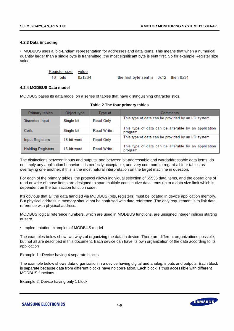
MODBUS bases its data model on a series of tables that have distinguishing characteristics.
Table 2 The four primary tables
The distinctions between inputs and outputs, and between bit-addressable and wordaddressable data items, do not imply any application behavior. It is perfectly acceptable, and very common, to regard all four tables as overlaying one another, if this is the most natural interpretation on the target machine in question.
For each of the primary tables, the protocol allows individual selection of 65536 data items, and the operations of read or write of those items are designed to span multiple consecutive data items up to a data size limit which is dependent on the transaction function code.
It’s obvious that all the data handled via MODBUS (bits, registers) must be located in device application memory. But physical address in memory should not be confused with data reference. The only requirement is to link data reference with physical address.
MODBUS logical reference numbers, which are used in MODBUS functions, are unsigned integer indices starting at zero.
• Implementation examples of MODBUS model
The examples below show two ways of organizing the data in device. There are different organizations possible, but not all are described in this document. Each device can have its own organization of the data according to its application
Example 1 : Device having 4 separate blocks
The example below shows data organization in a device having digital and analog, inputs and outputs. Each block is separate because data from different blocks have no correlation. Each block is thus accessible with different MODBUS functions.
Example 2: Device having only 1 block

S3FM02G429_AN_REV 1.00 4 MOTOR MONITORING SYSTEM BY S3FN429
4-7
In this example, the device has only 1 data block. The same data can be reached via several MODBUS functions, either via a 16 bit access or via an access bit.
Figure 4- 5 MODBUS Data Model with separate block
Figure 4- 6 MODBUS Data Model with only 1 block

S3FM02G429_AN_REV 1.00 4 MOTOR MONITORING SYSTEM BY S3FN429
4-8
4.3 Initialization
For initialization, port setting is needed at first. The Figure 4-7 shows the port setting by pressing the port open/close button. Baud rate is fixed to 19200bps. And, other parameter (data bit, parity bit, stop bit) are 8,n,1.
After port setting, device should be selected by radio button among devices. With this device selection, Default Monitoring Parameter and profile for sequence are set automatically. Auto command function uses this profile.
Figure 4- 7 Comport Setting
Figure 4- 8 Default Parameter Setting
S3FM02G429_AN_REV 1.00 4 MOTOR MONITORING SYSTEM BY S3FN429
4-9
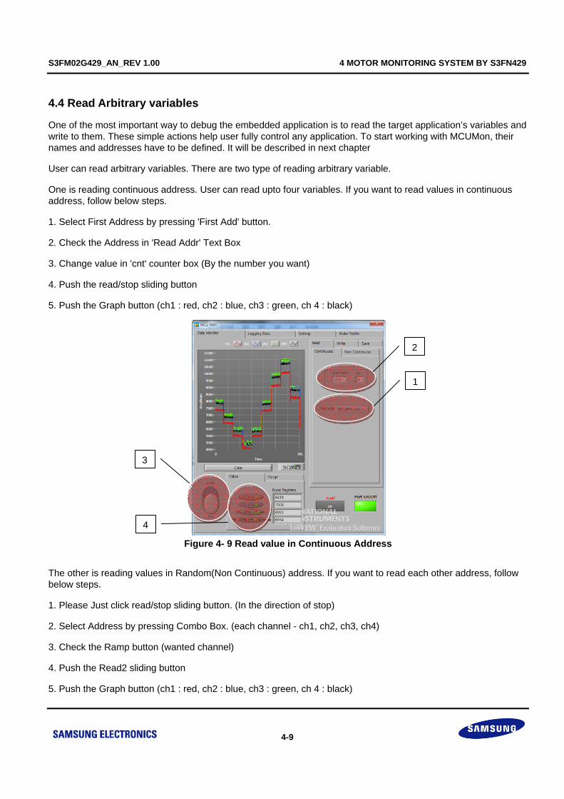
4.4 Read Arbitrary variables
One of the most important way to debug the embedded application is to read the target application’s variables and write to them. These simple actions help user fully control any application. To start working with MCUMon, their names and addresses have to be defined. It will be described in next chapter
User can read arbitrary variables. There are two type of reading arbitrary variable.
One is reading continuous address. User can read upto four variables. If you want to read values in continuous address, follow below steps.
1. Select First Address by pressing 'First Add' button.
2. Check the Address in 'Read Addr' Text Box
3. Change value in 'cnt' counter box (By the number you want)
4. Push the read/stop sliding button
5. Push the Graph button (ch1 : red, ch2 : blue, ch3 : green, ch 4 : black)
Figure 4- 9 Read value in Continuous Address
The other is reading values in Random(Non Continuous) address. If you want to read each other address, follow below steps.
1. Please Just click read/stop sliding button. (In the direction of stop)
2. Select Address by pressing Combo Box. (each channel - ch1, ch2, ch3, ch4)
3. Check the Ramp button (wanted channel)
4. Push the Read2 sliding button
5. Push the Graph button (ch1 : red, ch2 : blue, ch3 : green, ch 4 : black)
1
2
3
4

S3FM02G429_AN_REV 1.00 4 MOTOR MONITORING SYSTEM BY S3FN429
4-10
Figure 4- 10 Read value in Random Address
A Continuous address Function is faster than a Random address Function because there are a lot of steps on Reading Random address. This is Modbus feature. Below picture describes this feature.
Figure 4- 11 Ramdom Address Function (1cycle)
5
3
4 1
2
S3FM02G429_AN_REV 1.00 4 MOTOR MONITORING SYSTEM BY S3FN429
4-11
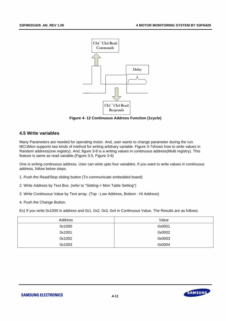
Figure 4- 12 Continuous Address Function (1cycle)
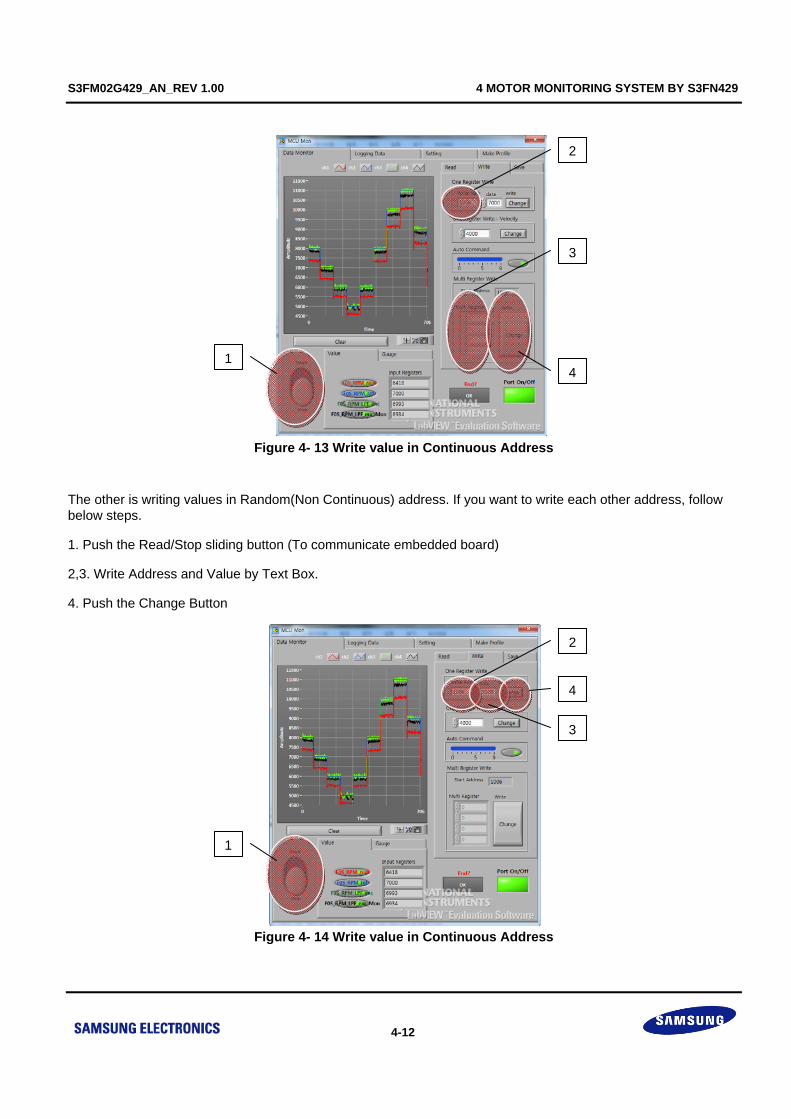
4.5 Write variables
Many Parameters are needed for operating motor. And, user wants to change parameter during the run. MCUMon supports two kinds of method for writing arbitrary variable. Figure 3-7shows how to write values in Random address(one registry). And, figure 3-8 is a writing values in continuous address(Multi registry). This feature is same as read variable.(Figure 3-5, Figure 3-6)
One is writing continuous address. User can wirte upto four variables. If you want to write values in continuous address, follow below steps.
1. Push the Read/Stop sliding button (To communicate embedded board)
2. Write Address by Text Box. (refer to "Setting-> Mon Table Setting")
3. Write Continuous Value by Text array. (Top : Low Address, Bottom : HI Address)
4. Push the Change Button.
Ex) If you write 0x1000 in address and 0x1, 0x2, 0x3, 0x4 in Continuous Value, The Results are as follows.
Address Value
0x1000 0x0001
0x1001 0x0002
0x1002 0x0003
0x1003 0x0004
S3FM02G429_AN_REV 1.00 4 MOTOR MONITORING SYSTEM BY S3FN429
4-12
Figure 4- 13 Write value in Continuous Address
The other is writing values in Random(Non Continuous) address. If you want to write each other address, follow below steps.
1. Push the Read/Stop sliding button (To communicate embedded board)
2,3. Write Address and Value by Text Box.
4. Push the Change Button
Figure 4- 14 Write value in Continuous Address
1
2
3
4
1
2
3
4
S3FM02G429_AN_REV 1.00 4 MOTOR MONITORING SYSTEM BY S3FN429
4-13
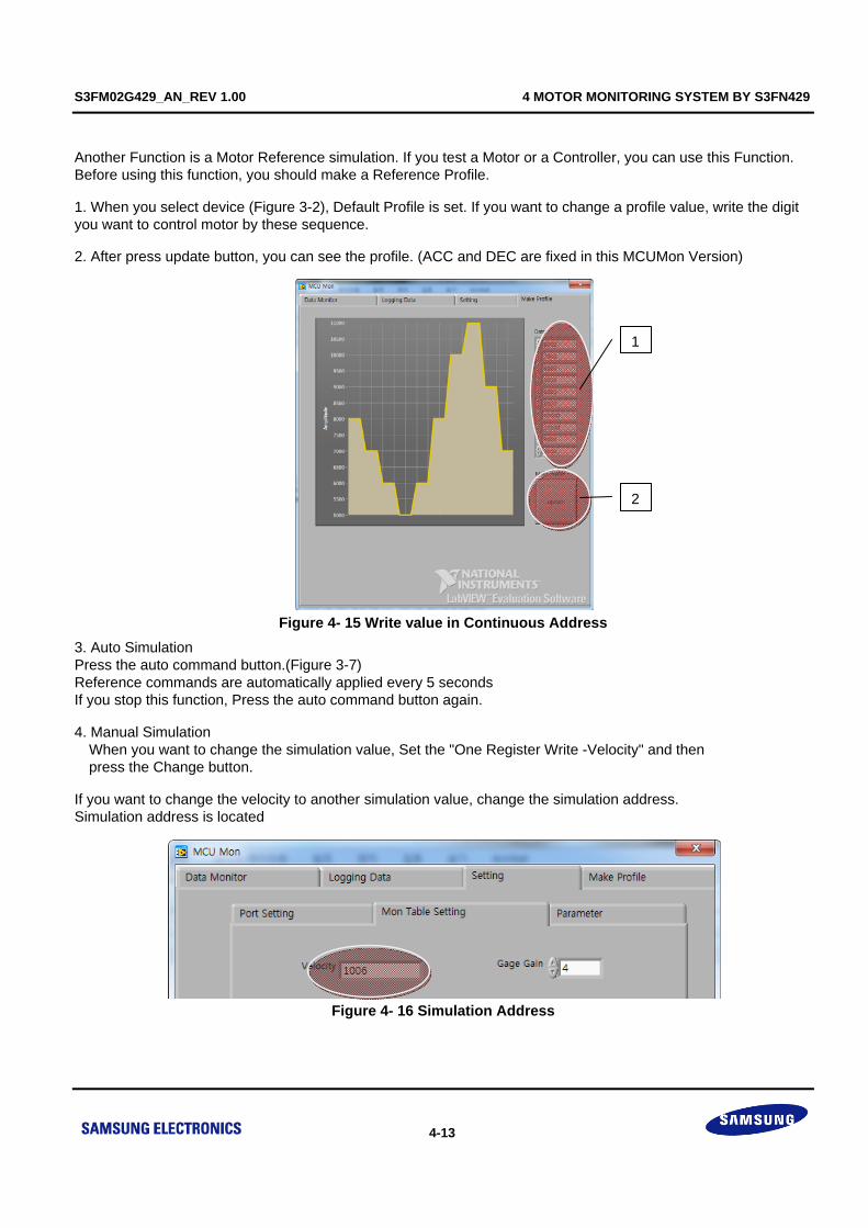
Another Function is a Motor Reference simulation. If you test a Motor or a Controller, you can use this Function. Before using this function, you should make a Reference Profile.
1. When you select device (Figure 3-2), Default Profile is set. If you want to change a profile value, write the digit you want to control motor by these sequence.
2. After press update button, you can see the profile. (ACC and DEC are fixed in this MCUMon Version)
Figure 4- 15 Write value in Continuous Address
3. Auto Simulation Press the auto command button.(Figure 3-7) Reference commands are automatically applied every 5 seconds If you stop this function, Press the auto command button again.
4. Manual Simulation When you want to change the simulation value, Set the "One Register Write -Velocity" and then press the Change button.
If you want to change the velocity to another simulation value, change the simulation address. Simulation address is located
Figure 4- 16 Simulation Address
1
2

S3FM02G429_AN_REV 1.00 4 MOTOR MONITORING SYSTEM BY S3FN429
4-14
4.6 Save variables
There are two ways about saving a Graph. When you want to save graph, locate mouse cursor at graph and then press right button. If pop up appear, select "export -> export data to excel"
Figure 4- 17 Save the graph1
Another way is using a save function. The Save Function is located in Data Monitor Tab. You can use this function at any time during monitoring. Saved file format is "Mon_Log.xls". Location is "D:\" The details are as follows: (Two Functions are not available at the same time) 1. Auto Save - When you push toggle switch, It will be saved in the specified path and name. 2. Edge Save - First, Set the Edge Value for each channel. Then, Push the slide button. When the edge condition is met, the data will be saved
Figure 4- 18 Save the graph2
1 1
2

S3FM02G429_AN_REV 1.00 4 MOTOR MONITORING SYSTEM BY S3FN429
4-15
4.7 Load Logging Data
User can read log data in the MCU. While the state of motor(certain address in the SRAM of MCU) can be read by this function.
1. Write a start address and total counts for data. 2. Click the Read Data Button. 3. The graph is saved automatically. (path:D:\ Log_Data.xls)
Figure 4- 19 Load Logging Data.
4.8 Other Feature
1. Gauge Display
2. Graph Control , PC Registry Read and Write
1
2

S3FM02G429_AN_REV 1.00 5 APPLICATION SETUP
5-16
5 Application Setup
5.1 Introduction
This application exercises control of BLDC speed control without Hall effect sensors using the S3FN429.
5.2 Connection
Figue 5-1 shows the BLDC demo set of S3FN429 and its basic system connections.
• 20-pin Header connector (J2)— It is used to program and debug the MCU with this application software, or other software via uVision4.
• J1 Is the powered PWM output to the BLDC motor and Hall signal lines.
• P1 is UART connector
• CN1 is power input connector from DC power source(+24V)
• J3 is jumper setting for between hall sensor or UART Rx/Tx and GPIO ports (P0.19, P0.20, P0.21)
• J4 is jumper setting for between zero-crossing signal or hall sensor and comparator positive inputs
Figure 5- 1A Demo set

S3FM02G429_AN_REV 1.00 5 APPLICATION SETUP
5-17
JTAG interface
3phaseBLDC
MCU
DC/DC converter(24V 5V/15V)
Zero-crossing detection circuit
Figure 5- 2B System Connection
You can select the operation mode(BLDC speed control with/without hall sensor) by setting J4, and in order to monitor motor drive system you must set J3 jumper connection UART Rx/Tx with P0.20/P0.21.
This application operates in an environment that includes only +24 voltage and rotating machinery. Be aware that the power stage and control board are electrically common ground.
The Run/Stop switch has a function to be enable/disable PWM output for BLDC motor. There are 3 push buttons on the board. The Reset button is the reset switch, the Up button is performed for motor speed increase and the Down button is the command for motor speed decrease.
5.3 Application Outline
The system is designed to drive 3-pahse BLDC Motor. The application has the following specifications:
• BLDC speed control without hall sensor(120 degree commutation)
• 24V DC Supply
• Targeted for S3FN429 motor control board
• Running on 3-phase BLDC at 24V, 3-Phase DC Low-Voltage Power Stage
• Speed control loop(speed up/down)
• Maximum speed of 2500 rpm
• Manual interface (PWM ON/OFF switch, UP/DOWN push buttons control, LED indication for status)
• Over-voltage, under-voltage, over-current fault protection
• Hardware fault detection

S3FM02G429_AN_REV 1.00 5 APPLICATION SETUP
5-18
5.4 References
[1] T.Kenjo, "Permanent Magnet and Brushless DC Motors", Oxford, 1985
[2] T.J.E. Miller, "Brushless permanent magnet and reluctance motor drive", Oxford, 1989
[3] T.Kikuchi, T.Kenjo, "Remote Laboratory for a Brushless Dc Motor", IEEE Trans on Education, vol.44, no.2,
Mar.2001.
[4] Bimal K. Bose, " Power Electronics and Variable Frequency Drives Technology and Applications", IEEE Press,
ISBN 0-7803-1084-5, 1997
[5] Ned Mohan, " Advanced Electric Drives, Analysis, Control and Modeling using Simulink", MNPERE, ISBN 0-9715292-0-5, 2001
[6] Modbus-IDA, " US Application Protocol Specification V1.1b ", December 28, 2006
Related Documents