10 12 Interface to Microcontroller 1 μF 1 μF M 1 2 3 4 5 6 7 8 9 11 24 23 22 21 20 19 18 17 16 15 14 13 VCP CPP CPN SW SWGND VREG V1P8 GND V3P3 SCL SDA FG VCC VCC W W V V U U PGND PGND DIR SPEED 0.1 μF 0.1 μF 3.3 V/5 V 47 μH 10 μF 10 μF VCC Copyright © 2016, Texas Instruments Incorporated Product Folder Order Now Technical Documents Tools & Software Support & Community Reference Design An IMPORTANT NOTICE at the end of this data sheet addresses availability, warranty, changes, use in safety-critical applications, intellectual property matters and other important disclaimers. PRODUCTION DATA. DRV10983, DRV10983Z SLVSCP6G – JULY 2014 – REVISED FEBRUARY 2018 DRV10983 12- to 24-V, Three-Phase, Sensorless BLDC Motor Driver 1 1 Features 1• Input Voltage Range: 8 to 28 V • Total Driver H + L r DS(on) : 250 mΩ • Drive Current: 2-A Continuous Winding Current (3-A Peak) • Sensorless Proprietary Back Electromotive Force (BEMF) Control Scheme • Continuous Sinusoidal 180° Commutation • No External Sense Resistor Required • For Flexibility User May Include External Sense Resistor to Monitor Power Delivered to Motor • Flexible User Interface Options: – I 2 C Interface: Access Registers for Command and Feedback – Dedicated SPEED Pin: Accepts Either Analog or PWM Input – Dedicated FG Pin: Provides TACH Feedback – Spin-Up Profile Customizable With EEPROM – Forward-Reverse Control With DIR Pin • Integrated Step-Down Regulator to Efficiently Provide Voltage (5 V or 3.3 V) for Internal and External Circuits • Supply Current 3 mA With Standby Version (DRV10983) • Supply Current 180 μA With Sleep Version (DRV10983Z) • Overcurrent Protection • Lock Detection • Voltage Surge Protection • UVLO Protection • Thermal Shutdown Protection • Thermally-Enhanced 24-Pin HTSSOP 2 Applications • Appliance Fan • HVAC 3 Description The DRV10983 device is a three-phase sensorless motor driver with integrated power MOSFETs, which can provide continuous drive current up to 2 A. The device is specifically designed for cost-sensitive, low- noise, low-external-component-count applications. The DRV10983 device uses a proprietary sensorless control scheme to provide continuous sinusoidal drive, which significantly reduces the pure tone acoustics that typically occur as a result of commutation. The interface to the device is designed to be simple and flexible. The motor can be controlled directly through PWM, analog, or I 2 C inputs. Motor speed feedback is available through either the FG pin or I 2 C. The DRV10983 device features an integrated step- down regulator to efficiently step down the supply voltage to either 5 or 3.3 V for powering both internal and external circuits. The device is available in either a sleep mode or a standby mode version to conserve power when the motor is not running. The standby mode (3-mA) version leaves the regulator running and the sleep mode (180-μA) version shuts it off. Use the standby mode version in applications where the regulator is used to power an external microcontroller. Device Information (1) PART NUMBER PACKAGE BODY SIZE (NOM) DRV10983 HTSSOP (24) 7.80 mm × 6.40 mm DRV10983Z (1) For all available packages, see the orderable addendum at the end of the data sheet. Application Schematic

Welcome message from author
This document is posted to help you gain knowledge. Please leave a comment to let me know what you think about it! Share it to your friends and learn new things together.
Transcript

10
12Interface to
Microcontroller
1 µF
1 µF
M
1
2
3
4
5
6
7
8
9
11
24
23
22
21
20
19
18
17
16
15
14
13
VCP
CPP
CPN
SW
SWGND
VREG
V1P8
GND
V3P3
SCL
SDA
FG
VCC
VCC
W
W
V
V
U
U
PGND
PGND
DIR
SPEED
0.1 µF
0.1 µF
3.3 V/5 V
47 µH
10 µF
10 µF
VCC
Copyright © 2016, Texas Instruments Incorporated
Product
Folder
Order
Now
Technical
Documents
Tools &
Software
Support &Community
ReferenceDesign
An IMPORTANT NOTICE at the end of this data sheet addresses availability, warranty, changes, use in safety-critical applications,intellectual property matters and other important disclaimers. PRODUCTION DATA.
DRV10983, DRV10983ZSLVSCP6G –JULY 2014–REVISED FEBRUARY 2018
DRV10983 12- to 24-V, Three-Phase, Sensorless BLDC Motor Driver
1
1 Features1• Input Voltage Range: 8 to 28 V• Total Driver H + L rDS(on): 250 mΩ• Drive Current: 2-A Continuous Winding Current
(3-A Peak)• Sensorless Proprietary Back Electromotive Force
(BEMF) Control Scheme• Continuous Sinusoidal 180° Commutation• No External Sense Resistor Required• For Flexibility User May Include External Sense
Resistor to Monitor Power Delivered to Motor• Flexible User Interface Options:
– I2C Interface: Access Registers for Commandand Feedback
– Dedicated SPEED Pin: Accepts Either Analogor PWM Input
– Dedicated FG Pin: Provides TACH Feedback– Spin-Up Profile Customizable With EEPROM– Forward-Reverse Control With DIR Pin
• Integrated Step-Down Regulator to EfficientlyProvide Voltage (5 V or 3.3 V) for Internal andExternal Circuits
• Supply Current 3 mA With Standby Version(DRV10983)
• Supply Current 180 μA With Sleep Version(DRV10983Z)
• Overcurrent Protection• Lock Detection• Voltage Surge Protection• UVLO Protection• Thermal Shutdown Protection• Thermally-Enhanced 24-Pin HTSSOP
2 Applications• Appliance Fan• HVAC
3 DescriptionThe DRV10983 device is a three-phase sensorlessmotor driver with integrated power MOSFETs, whichcan provide continuous drive current up to 2 A. Thedevice is specifically designed for cost-sensitive, low-noise, low-external-component-count applications.
The DRV10983 device uses a proprietary sensorlesscontrol scheme to provide continuous sinusoidaldrive, which significantly reduces the pure toneacoustics that typically occur as a result ofcommutation. The interface to the device is designedto be simple and flexible. The motor can be controlleddirectly through PWM, analog, or I2C inputs. Motorspeed feedback is available through either the FG pinor I2C.
The DRV10983 device features an integrated step-down regulator to efficiently step down the supplyvoltage to either 5 or 3.3 V for powering both internaland external circuits. The device is available in eithera sleep mode or a standby mode version to conservepower when the motor is not running. The standbymode (3-mA) version leaves the regulator runningand the sleep mode (180-µA) version shuts it off. Usethe standby mode version in applications where theregulator is used to power an external microcontroller.
Device Information(1)
PART NUMBER PACKAGE BODY SIZE (NOM)DRV10983
HTSSOP (24) 7.80 mm × 6.40 mmDRV10983Z
(1) For all available packages, see the orderable addendum atthe end of the data sheet.
Application Schematic

2
DRV10983, DRV10983ZSLVSCP6G –JULY 2014–REVISED FEBRUARY 2018 www.ti.com
Product Folder Links: DRV10983
Submit Documentation Feedback Copyright © 2014–2018, Texas Instruments Incorporated
Table of Contents1 Features .................................................................. 12 Applications ........................................................... 13 Description ............................................................. 14 Revision History..................................................... 25 Description (continued)......................................... 46 Pin Configuration and Functions ......................... 47 Specifications......................................................... 5
7.1 Absolute Maximum Ratings ...................................... 57.2 ESD Ratings.............................................................. 57.3 Recommended Operating Conditions....................... 67.4 Thermal Information .................................................. 67.5 Electrical Characteristics........................................... 77.6 Typical Characteristics ............................................ 10
8 Detailed Description ............................................ 118.1 Overview ................................................................. 118.2 Functional Block Diagram ....................................... 128.3 Feature Description................................................. 138.4 Device Functional Modes........................................ 16
8.5 Register Maps ......................................................... 419 Application and Implementation ........................ 47
9.1 Application Information............................................ 479.2 Typical Application .................................................. 47
10 Power Supply Recommendations ..................... 4911 Layout................................................................... 49
11.1 Layout Guidelines ................................................. 4911.2 Layout Example .................................................... 50
12 Device and Documentation Support ................. 5112.1 Device Support .................................................... 5112.2 Documentation Support ........................................ 5112.3 Trademarks ........................................................... 5112.4 Electrostatic Discharge Caution............................ 5112.5 Receiving Notification of Documentation Updates 5112.6 Community Resources.......................................... 5112.7 Glossary ................................................................ 51
13 Mechanical, Packaging, and OrderableInformation ........................................................... 51
4 Revision HistoryNOTE: Page numbers for previous revisions may differ from page numbers in the current version.
Changes from Revision F (December 2017) to Revision G Page
• Added timing information for entering and exiting sleep mode and standby mode ............................................................... 8• Added BEMF COMPARATOR hysteresis specification ......................................................................................................... 9• Updated Start the Motor Under Different Initial Conditions figure ........................................................................................ 20• Changed the default value for register address 0x27 from 0xFC to 0xF4 in the Default EEPROM Value table ................. 42• Deleted the "TI recommends..." sentence from the description for address 0x27, bit 3 ...................................................... 45• Added constraints to recommended external inductor ......................................................................................................... 48
Changes from Revision E (May 2017) to Revision F Page
• Added the internal SPEED pin pulldown resistance to ground parameter to the Electrical Characteristics table ................. 8• Changed the Step-Down Regulator section ......................................................................................................................... 13• Updated the Motor Phase Resistance section ..................................................................................................................... 16• Deleted the Inductive AVS Function section ........................................................................................................................ 36• Changed the default value for register address 0x29 from 0xB7 to 0xB9 in the Default EEPROM Value table ................. 42• Added application information for the sleep mode device ................................................................................................... 47
Changes from Revision D (May 2017) to Revision E Page
• Changed pin numbering in the Pin Functions table .............................................................................................................. 4
Changes from Revision C (May 2016) to Revision D Page
• Added the DRV10983Z part number to the data sheet header and to the Device Information table .................................... 1• Added DRV10983Z part number ............................................................................................................................................ 6• Corrected the link to the DRV10983 and DRV10975 Tuning Guide .................................................................................... 16• Added text to the PWM Output section ................................................................................................................................ 36

3
DRV10983, DRV10983Zwww.ti.com SLVSCP6G –JULY 2014–REVISED FEBRUARY 2018
Product Folder Links: DRV10983
Submit Documentation FeedbackCopyright © 2014–2018, Texas Instruments Incorporated
• Changed Figure 37............................................................................................................................................................... 37• Changed "FGOLSet[1:0]" to "FGOLsel[1:0]" in Register Map address 0x2B....................................................................... 41• Added recommended minimum dead time to SysOpt7 register........................................................................................... 46• Added External Components table ...................................................................................................................................... 48• Changed the link to the DRV10983 and DRV10975 Tuning Guide ..................................................................................... 48• Changed the layout example................................................................................................................................................ 50
Changes from Revision B (February 2015) to Revision C Page
• Added "phase to phase" clarification for overcurrent protection............................................................................................. 9• Added more accurate description to clarify overcurrent protection operation ...................................................................... 14
Changes from Revision A (October 2014) to Revision B Page
• Updated data sheet with the DRV10983Z sleep version ...................................................................................................... 1
Changes from Original (July 2014) to Revision A Page
• Updated the input voltage range: 8 to 28 V............................................................................................................................ 1• Removed DRV10983Z sleep version part and updated standby mode supply current ......................................................... 1• Updated pin information for SW, SWGND, VREG, SDA, FG, and VCC pins ........................................................................ 4• Added DIR, SW, and VREG pins to Absolute Maximum Ratings ......................................................................................... 5• Updated max supply voltage and voltage range ratings for VCC and U, V, W in Recommended Operating Conditions ..... 5• changed Functional Block Diagram ..................................................................................................................................... 12• Changed "hardware current limit" to "lock detection current limit" and "software current" to "acceleration current
limit" throughout data sheet .................................................................................................................................................. 14• Updated max value for open to closed loop threshold ........................................................................................................ 26• Corrected description to "velocity constant of the motor" for Equation 2 ............................................................................ 26• Corrected register name in Start-Up Current Setting .......................................................................................................... 26• Updated Equation 3 ............................................................................................................................................................. 26• Updated Figure 20 ............................................................................................................................................................... 27• Updated caption name for Figure 24 ................................................................................................................................... 29• Corrected max speed command setting for SpdCtrl[8:0] .................................................................................................... 29• Updated register description for status register. .................................................................................................................. 41• Updated the data in the examples for MotorSpeed1 and MotorPeriod1 ............................................................................. 43• Updated IPDPosition description in Register Map .............................................................................................................. 43• Increased max motor voltage for Recommended Application Range ................................................................................. 48• Updated graph callout for Figure 41 .................................................................................................................................... 49

1VCP 24 VCC
2CPP 23 VCC
3CPN 22 W
4SW 21 W
5SWGND 20 V
6VREG 19 V
7V1P8 18 U
8GND 17 U
9V3P3 16 PGND
10SCL 15 PGND
11SDA 14 DIR
12FG 13 SPEED
Not to scale
Thermal pad (GND)
4
DRV10983, DRV10983ZSLVSCP6G –JULY 2014–REVISED FEBRUARY 2018 www.ti.com
Product Folder Links: DRV10983
Submit Documentation Feedback Copyright © 2014–2018, Texas Instruments Incorporated
(1) I = input, O = output, I/O = input/output, P = power
5 Description (continued)An I2C interface allows the user to reprogram specific motor parameters in registers and program the EEPROMto help optimize the performance for a given application. The DRV10983 device is available in a thermallyefficient HTSSOP, 24-pin package with an exposed thermal pad. The operating temperature is specified from–40°C to 125°C.
6 Pin Configuration and Functions
PWP PowerPAD™ Package24-Pin HTSSOP
Top View
Pin FunctionsPIN
TYPE (1) DESCRIPTIONNAME NO.
VCP 1 P Charge pump output.CPN 3 P Charge pump pin 1, use a ceramic capacitor between CPN and CPP.CPP 2 P Charge pump pin 2, use a ceramic capacitor between CPN and CPP.DIR 14 I DirectionFG 12 O FG signal output.GND 8 — Digital and analog groundPGND 15, 16 — Power groundSCL 10 I I2C clock signalSDA 11 I/O I2C data signalSPEED 13 I Speed control signal for PWM or analog input speed commandSW 4 O Step-down regulator switching node outputSWGND 5 P Step-down regulator groundU 17, 18 O Motor U phaseV 19, 20 O Motor V phase

5
DRV10983, DRV10983Zwww.ti.com SLVSCP6G –JULY 2014–REVISED FEBRUARY 2018
Product Folder Links: DRV10983
Submit Documentation FeedbackCopyright © 2014–2018, Texas Instruments Incorporated
Pin Functions (continued)PIN
TYPE (1) DESCRIPTIONNAME NO.
V1P8 7 P Internal 1.8-V digital core voltage. V1P8 capacitor must connect to GND. This is an output, but notspecified to drive external loads.
V3P3 9 P Internal 3.3-V supply voltage. V3P3 capacitor must connect to GND. This is an output and may driveexternal loads not to exceed IV3P3_MAX.
VCC 23, 24 P Device power supplyVREG 6 P Step-down regulator output and feedback pointW 21, 22 O Motor W phasethermal pad(GND) — — The exposed thermal pad must be electrically connected to ground plane through soldering to PCB
for proper operation and connected to bottom side of PCB through vias for better thermal spreading.
(1) Stresses beyond those listed under Absolute Maximum Ratings may cause permanent damage to the device. These are stress ratingsonly, which do not imply functional operation of the device at these or any other conditions beyond those indicated under RecommendedOperating Conditions. Exposure to absolute-maximum-rated conditions for extended periods may affect device reliability.
(2) All voltage values are with respect to the network ground terminal unless otherwise noted.
7 Specifications
7.1 Absolute Maximum Ratingsover operating ambient temperature (unless otherwise noted) (1)
MIN MAX UNIT
Input voltage (2)
VCC –0.3 30
VSPEED –0.3 4GND –0.3 0.3SCL, SDA –0.3 4DIR –0.3 4
Output voltage (2)
U, V, W –1 30
V
SW –1 30VREG –0.3 7FG –0.3 4VCP –0.3 V(VCC) + 6CPN –0.3 30CPP –0.3 V(VCC) + 6V3P3 –0.3 4V1P8 –0.3 2.5
Maximum junction temperature, TJ_MAX –40 150 °CStorage temperature, Tstg –55 150 °C
(1) JEDEC document JEP155 states that 500-V HBM allows safe manufacturing with a standard ESD control process.(2) JEDEC document JEP157 states that 250-V CDM allows safe manufacturing with a standard ESD control process.
7.2 ESD RatingsVALUE UNIT
V(ESD)Electrostaticdischarge
Human body model (HBM), per ANSI/ESDA/JEDEC JS-001, all pins (1) ±2500V
Charged device model (CDM), per JEDEC specification JESD22-C101, all pins (2) ±1500

6
DRV10983, DRV10983ZSLVSCP6G –JULY 2014–REVISED FEBRUARY 2018 www.ti.com
Product Folder Links: DRV10983
Submit Documentation Feedback Copyright © 2014–2018, Texas Instruments Incorporated
7.3 Recommended Operating Conditionsover operating ambient temperature range (unless otherwise noted)
MIN NOM MAX UNITSupply voltage VCC 8 24 28 V
VoltageU, V, W –0.7 29
VSCL, SDA, FG, SPEED, DIR –0.1 3.3 3.6PGND, GND –0.1 0.1
CurrentStep-down regulator output current (buck mode) 100
mAStep-down regulator output current (linear mode) 0V3P3 LDO output current 5
Operating junction temperature, TJ –40 125 °C
(1) For more information about traditional and new thermal metrics, see the Semiconductor and IC Package Thermal Metrics applicationreport.
7.4 Thermal Information
THERMAL METRIC (1)DRV10983, DRV10983Z
UNITPWP (HTSSOP)24 PINS
RθJA Junction-to-ambient thermal resistance 36.1 °C/WRθJC(top) Junction-to-case (top) thermal resistance 17.4 °C/WRθJB Junction-to-board thermal resistance 14.8 °C/WψJT Junction-to-top characterization parameter 0.4 °C/WψJB Junction-to-board characterization parameter 14.5 °C/WRθJC(bot) Junction-to-case (bottom) thermal resistance 1.1 °C/W

7
DRV10983, DRV10983Zwww.ti.com SLVSCP6G –JULY 2014–REVISED FEBRUARY 2018
Product Folder Links: DRV10983
Submit Documentation FeedbackCopyright © 2014–2018, Texas Instruments Incorporated
7.5 Electrical Characteristicsover operating ambient temperature range (unless otherwise noted)
PARAMETER TEST CONDITIONS MIN TYP MAX UNITSUPPLY CURRENT (DRV10983)
IVcc Supply current
TA = 25°C; sleepDis = 1; SPEED = 0 V;V(VCC) = 24 V; buck regulator 3.5 5
mATA = 25°C; sleepDis = 1; SPEED = 0 V;V(VCC) = 24 V; linear regulator 11
IVccSTBY Standby current
TA = 25°C; SPEED = 0 V; V(VCC) = 24 V;standby mode device; buck regulator 3 4
mATA = 25°C; SPEED = 0 V; V(VCC) = 24 V;standby mode device; linear regulator 9
SUPPLY CURRENT (DRV10983Z)
IVcc Supply current
TA = 25°C; sleepDis = 1; SPEED = 0 V;V(VCC) = 24 V; buck regulator 3.5 5
mATA = 25°C; sleepDis = 1; SPEED = 0 V;V(VCC) = 24 V; linear regulator 11
IVccSLEEP Sleep current TA = 25°C; SPEED = 0 V; V(VCC) = 24 V;sleep mode device; buck regulator 160 200 µA
UVLOVUVLO_R UVLO threshold voltage Rise threshold, TA = 25°C 7 7.4 8 VVUVLO_F UVLO threshold voltage Fall threshold, TA = 25°C 6.7 7.1 7.5 V
VUVLO_HYSUVLO threshold voltagehysteresis TA = 25°C 200 300 400 mV
LDO OUTPUT
V3P3
V(VCC) = 24 V, TA = 25°C, VregSel = 0,5-mA load 3 3.3 3.6
VV(VCC) = 24 V, TA = 25°C, VregSel = 1,V(VREG) < 3.3 V, 5-mA load V(VREG) – 0.3 V(VREG) – 0.1 V(VREG)
V(VCC) = 24 V, TA = 25°C, VregSel = 1,V(VREG) ≥ 3.3 V, 5-mA load 3 3.3 3.6
IV3P3_MAX Maximum load from V3P3 V(VCC) = 24 V, TA = 25°C 5 mA
V1P8V(VCC) = 24 V, TA = 25°C, VregSel = 0 1.6 1.78 2
VV(VCC) = 24 V, TA = 25°C, VregSel = 1 1.6 1.78 2
STEP-DOWN REGULATOR
VREG Regulator output voltage
TA = 25˚C; VregSel = 0, LSW = 47 µH,CSW = 10 µF, Iload = 50 mA 4.5 5 5.5
VTA = 25˚C; VregSel = 1, LSW = 47 µH,CSW = 10 µF, Iload = 50 mA 3.06 3.4 3.6
VREG_LRegulator output voltage(linear mode)
TA = 25°C, VregSel = 0, RSW = 39 Ω,CSW = 10 µF 5
VTA = 25°C, VregSel = 1, RSW = 39 Ω,CSW = 10 µF 3.4
IREG_MAX Maximum load from VREG TA = 25°C, LSW = 47 µH, CSW = 10 µF 100 mAINTEGRATED MOSFET
rDS(on) Series resistance (H + L)
TA = 25˚C; V(VCC) = 24 V; V(VCP) = 29 V;Iout = 1 A 0.25 0.4
ΩTA = 85˚C; V(VCC) = 24 V; V(VCP) = 29 V;Iout = 1 A 0.325
SPEED – ANALOG MODEVAN/A_FS Analog full speed voltage V(V3P3) × 0.9 VVAN/A_ZS Analog zero speed voltage 100 mVtSAM Analog speed sample period 320 µsVAN/A_RES Analog voltage resolution 5.8 mVSPEED – PWM DIGITAL MODE

8
DRV10983, DRV10983ZSLVSCP6G –JULY 2014–REVISED FEBRUARY 2018 www.ti.com
Product Folder Links: DRV10983
Submit Documentation Feedback Copyright © 2014–2018, Texas Instruments Incorporated
Electrical Characteristics (continued)over operating ambient temperature range (unless otherwise noted)
PARAMETER TEST CONDITIONS MIN TYP MAX UNITVDIG_IH PWM input high voltage 2.2 VVDIG_IL PWM input low voltage 0.6 VƒPWM PWM input frequency 1 100 kHz
STANDBY MODE (DRV10983)
VEN_SBAnalog voltage-to-enterstandby mode SpdCtrlMd = 0 (analog mode) 30 mV
VEX_SBAnalog voltage-to-exitstandby SpdCtrlMd = 0 (analog mode) 120 mV
tEX_SB_ANATime-to-exit from standbymode
SpdCtrlMd = 0 (analog mode)SPEED > VEX_SB
700 ms
tEX_SB_DR_ANA
Time taken to drive motorafter exiting from standbymode
SpdCtrlMd = 0 (analog mode)SPEED > VEX_SL; ISDen = 0;BrkDoneThr[2:0] = 0
1 µs
tEX_SB_PWM
Time-to-exit from standbymode
SpdCtrlMd = 1 (PWM mode)SPEED > VDIG_IH
1 µs
tEX_SB_DR_PWM
Time taken to drive motorafter exiting from standbymode
SpdCtrlMd = 1 (PWM mode)SPEED > VDIG_IH; ISDen = 0; BrkDoneThr[2:0] =0
55 ms
tEN_SB_ANA Time-to-enter sleep mode SpdCtrlMd = 0 (analog mode)SPEED < VEN_SL; AvSIndEn = 0 5 ms
tEN_SB_PWM
Time-to-enter sleep mode SpdCtrlMd = 1 (PMW mode)SPEED < VDIG_IL; AvSIndEn = 0 60 ms
SLEEP MODE (DRV10983Z)VEN_SL Analog voltage-to-enter sleep SpdCtrlMd = 0 (analog mode) 30 mVVEX_SL Analog voltage-to-exit sleep SpdCtrlMd = 0 (analog mode) 2.2 3.3 V
tEX_SL_ANA Time-to-exit from sleep mode SpdCtrlMd = 0 (analog mode)SPEED > VEX_SL
1 µs
tEX_SL_DR_ANA
Time taken to drive motorafter exiting from sleep mode
SpdCtrlMd = 0 (analog mode)SPEED > VEX_SL; ISDen = 0;BrkDoneThr[2:0] = 0
350 µs
tEX_SL_PWM Time-to-exit from sleep mode SpdCtrlMd = 1 (PWM mode)SPEED > VDIG_IH
1 µs
tEX_SL_DR_PWM
Time taken to drive motorafter exiting from sleep mode
SpdCtrlMd = 1 (PWM mode)SPEED > VDIG_IH; ISDen = 0; BrkDoneThr[2:0] =0
350 ms
tEN_SL_ANA Time-to-enter sleep mode SpdCtrlMd = 0 (analog mode)SPEED < VEN_SL; AvSIndEn = 0 5.2 ms
tEN_SL_PWM Time-to-enter sleep mode SpdCtrlMd = 1 (PMW mode)SPEED < VDIG_IL; AvSIndEn = 0 58 ms
RPD_SPEED_SL
Internal SPEED pin pulldownresistance to ground VSPEED = 0 (sleep mode) 55 kΩ
DIGITAL I/O (DIR INPUT AND FG OUTPUT)VDIR_H Input high 2.2 VVDIR_L Input low 0.6 VIFG_SINK Output sink current Vout = 0.3 V 5 mAI2C SERIAL INTERFACEVI2C_H Input high 2.2 VVI2C_L Input low 0.6 VLOCK DETECTION RELEASE TIMEtLOCK_OFF Lock release time 5 stLCK_ETR Lock enter time 0.3 sOVERCURRENT PROTECTION

9
DRV10983, DRV10983Zwww.ti.com SLVSCP6G –JULY 2014–REVISED FEBRUARY 2018
Product Folder Links: DRV10983
Submit Documentation FeedbackCopyright © 2014–2018, Texas Instruments Incorporated
Electrical Characteristics (continued)over operating ambient temperature range (unless otherwise noted)
PARAMETER TEST CONDITIONS MIN TYP MAX UNITIOC_limit Overcurrent protection TA = 25˚C; phase to phase 3 4 ATHERMAL SHUTDOWN
TSDNShutdown temperaturethreshold Shutdown temperature 150 °C
TSDN_HYSShutdown temperaturethreshold Hysteresis 10 °C
BEMF COMPARATORBEMFHYS BEMF comparator hysteresis bemfHsyEn = 1 50 mV

Power Supply
Sw
itchi
ng R
egul
ator
Out
put
0 10 20 303.1
3.2
3.3
3.4
3.5
D004
VREG
Power Supply
Sup
ply
Cur
rent
0 10 20 300
0.002
0.004
0.006
0.008
D001
IVCC
Power Supply
Sw
itchi
ng R
egul
ator
Out
put
0 10 20 304.8
4.9
5
5.1
5.2
D002
VREG
10
DRV10983, DRV10983ZSLVSCP6G –JULY 2014–REVISED FEBRUARY 2018 www.ti.com
Product Folder Links: DRV10983
Submit Documentation Feedback Copyright © 2014–2018, Texas Instruments Incorporated
7.6 Typical Characteristics
Figure 1. Supply Current vs Power Supply Figure 2. Step-down Regulator Output vs Power Supply(VregSel = 0)
Figure 3. Step-down Regulator Output vs Power Supply(VregSel = 1)

11
DRV10983, DRV10983Zwww.ti.com SLVSCP6G –JULY 2014–REVISED FEBRUARY 2018
Product Folder Links: DRV10983
Submit Documentation FeedbackCopyright © 2014–2018, Texas Instruments Incorporated
8 Detailed Description
8.1 OverviewThe DRV10983 is a three-phase sensorless motor driver with integrated power MOSFETs, which provide drivecurrent capability up to 2 A continuous. The device is specifically designed for low-noise, low external componentcount, 12- to 24-V motor drive applications. The device is configurable through a simple I2C interface toaccommodate different motor parameters and spin-up profiles for different customer applications.
A 180° sensorless control scheme provides continuous sinusoidal output voltages to the motor phases to enableultra-quiet motor operation by keeping the electrically induced torque ripple small.
The DRV10983 features extensive protection and fault detect mechanisms to ensure reliable operation. Voltagesurge protection prevents the input Vcc capacitor from overcharging, which is typical during motor deceleration.The devices provides phase to phase overcurrent protection without the need for an external current senseresistor. Rotor lock detect is available through several methods. These methods can be configured with registersettings to ensure reliable operation. The device provides additional protection for undervoltage lockout (UVLO)and for thermal shutdown.
The commutation control algorithm continuously measures the motor phase current and periodically measuresthe VCC supply voltage. The device uses this information for BEMF estimation, and the information is alsoprovided through the I2C register interface for debug and diagnostic use in the system, if desired.
A buck step-down regulator efficiently steps down the supply voltage. The output of this regulator provides powerfor the internal circuits and can also be used to provide power for an external circuit such as a microcontroller. Ifproviding power for an external circuit is not necessary (and to reduce system cost), configure the buck step-down regulator as a linear regulator by replacing the inductor with resistor.
TI designed the interfacing to the DRV10983 to be flexible. In addition to the I2C interface, the system can usethe discrete FG pin, DIR pin, and SPEED pin. SPEED is the speed command input pin. It controls the outputvoltage amplitude. DIR is the direction control input pin. FG is the speed indicator output, which shows thefrequency of the motor commutation.
EEPROM is integrated in the DRV10983 as memory for the motor parameter and operation settings. EEPROMdata transfers to the register after power on and exit from sleep mode.
The DRV10983 device can also operate in register mode. If the system includes a microcontroller communicatingthrough the I2C interface, the device can dynamically update the motor parameter and operation settings bywriting to the registers. In this configuration, the EEPROM data is bypassed by the register settings.
V/I sensor
VCC
PGND
LogicCore
UVW
UVLO
Over Current
Lock
Charge Pump
Thermal
WPre -Driver
VCPVCC
VPre -Driver
PGND
VCPVCC
UPre -Driver
PGND
VCPVCC
PWM and Analog Speed Control
FG
SDA
SCL
Oscillator
Bandgap
3.3-/5-V Step-Down Regulator
SW
VREG
3.3-V LDO
1.8-V LDO
V3P3
V1P8
SPEED
ADC
CPP
CPN
VCP
GND
I2C Communication
Register EEPROM
GND
SWGND
DIR
12
DRV10983, DRV10983ZSLVSCP6G –JULY 2014–REVISED FEBRUARY 2018 www.ti.com
Product Folder Links: DRV10983
Submit Documentation Feedback Copyright © 2014–2018, Texas Instruments Incorporated
8.2 Functional Block Diagram
VCC
SWGND
IC SW
VREG
3.3 V/5 V Load
47 µH
10 µF
VCC
SWGND
IC SW
VREG
3.3 V/5 V
39 Ω
10 µF
13
DRV10983, DRV10983Zwww.ti.com SLVSCP6G –JULY 2014–REVISED FEBRUARY 2018
Product Folder Links: DRV10983
Submit Documentation FeedbackCopyright © 2014–2018, Texas Instruments Incorporated
8.3 Feature Description
8.3.1 Regulators
8.3.1.1 Step-Down RegulatorThe DRV10983 includes a hysteretic step-down voltage regulator that can be operated as either a switching buckregulator using an external inductor or as a linear regulator using an external resistor (see Figure 4). The bestefficiency is achieved when the step-down regulator is in buck mode. However, the DRV10983Z device (sleepmode version) only operates with the step-down regulator in linear mode and with a Zener diode as described inthe Typical Application section. The regulator output voltage can be configured by register bit VregSel. WhenVregSel = 0, the regulator output voltage is 5 V, and when VregSel = 1, the regulator output voltage is 3.3 V.When the regulated voltage drops by the hysteresis level, the high-side FET turns on to increase the regulatedvoltage back to the target of 3.3 V or 5 V. The switching frequency of the hysteretic regulator is not constant andchanges with the load.
If the step-down regulator is configured in buck mode, see IREG_MAX in the Electrical Characteristics to determinethe amount of current provided for external load. If the step-down regulator is configured as linear mode, it isused for the device internal circuit only.
NOTEThe DRV10983Z step-down regulator only operates in linear mode (using an externalresistor) and with a Zener diode as described in the Typical Application section. TheDRV10983Z device does not support buck mode (using an external inductor) as shown inFigure 4.
Step-Down Regulator With External Inductor (BuckMode)
Step-Down Regulator With External Resistor (LinearMode)
Figure 4. Step-Down Regulator Configurations
8.3.1.2 3.3-V and 1.8-V LDOThe DRV10983 includes a 3.3-V LDO and an 1.8-V LDO. The 1.8-V LDO is for internal circuit only. The 3.3-VLDO is mainly for internal circuits, but can also drive external loads not to exceed IV3P3_MAX listed in the ElectricalCharacteristics. For example, it can work as a pullup voltage for the FG, DIR, SDA, and SCL interface.
Both V1P8 and V3P3 capacitor must be connected to GND.
8.3.2 Protection Circuits
8.3.2.1 Thermal ShutdownThe DRV10983 has a built-in thermal shutdown function, which shuts down the device when junctiontemperature is more than TSDN ˚C and recovers operating conditions when junction temperature falls to TSDN –TSDN_HYS˚C.
The OverTemp status bit (address 0x10 bit 7) is set during thermal shutdown.

PWM In
Analog
I2C
PWM_
DCO
AVS,
Acceleration Current Limit
Closed Loop Accelerate
PWM Duty
ADCSpeed
Command
Output
AmplitudeMotorVCC X
SPEED Pin
Copyright © 2017, Texas Instruments Incorporated
14
DRV10983, DRV10983ZSLVSCP6G –JULY 2014–REVISED FEBRUARY 2018 www.ti.com
Product Folder Links: DRV10983
Submit Documentation Feedback Copyright © 2014–2018, Texas Instruments Incorporated
Feature Description (continued)8.3.2.2 Undervoltage Lockout (UVLO)The DRV10983 has a built-in UVLO function block. The hysteresis of UVLO threshold is VUVLO-HYS. The device islocked out when VCC is down to VUVLO_F and woke up at VUVLO_R.
8.3.2.3 Overcurrent Protection (OCP)The overcurrent protection function acts to protect the device if the current, as measured from the FETs, exceedsthe IOC-limit threshold. It protects the device from phase-to-phase short-circuit conditions; the DRV10983 placesthe output drivers into a high-impedance state and maintains this condition until the overcurrent is no longerpresent. The OverCurr status bit (address 0x10 bit 5) is set.
The DRV10983 also provides acceleration current limit and lock detection current limit functions to protect thedevice and motor (see Current Limit and Lock Detect and Fault Handling).
8.3.2.4 LockWhen the motor is blocked or stopped by an external force, the lock protection is triggered, and the device stopsdriving the motor immediately. After the lock release time tLOCK_OFF, the DRV10983 resumes driving the motoragain. If the lock condition is still present, it enters the next lock protection cycle until the lock condition isremoved. With this lock protection, the motor and device does not get overheated or damaged due to the motorbeing locked (see Lock Detect and Fault Handling).
During lock condition, the MtrLck Status bit (address 0x10, bit 4) is set. To further diagnose, check the registerFaultCode.
8.3.3 Motor Speed ControlThe DRV10983 offers four methods for indirectly controlling the speed of the motor by adjusting the outputvoltage amplitude. This can be accomplished by varying the supply voltage (VCC) or by controlling the SpeedCommand. The Speed Command can be controlled in one of three ways. The user can set the Speed Commandon the SPEED pin by adjusting either the PWM input (SPEED pin configured for PWM mode) or the analog input(SPEED pin configured for analog mode), or by writing the Speed Command directly through the I2C serial portto SpdCtrl[8:0]. The Speed Command is used to determine the PWM duty cycle output (PWM_DCO) (seeFigure 5).
The Speed Command may not always be equal to the PWM_DCO because DRV10983 has implemented theAVS function (see AVS Function), the acceleration current limit function (see Acceleration Current Limit), and theclosed loop accelerate function (see Closed Loop Accelerate) to optimize the control performance. Thesefunctions can limit the PWM_DCO, which affects the output amplitude.
Figure 5. Multiplexing the Speed Command to the Output Amplitude Applied to the Motor
The output voltage amplitude applied to the motor is accomplished through sine wave modulation so that thephase-to-phase voltage is sinusoidal.

VCC
V / 2CC
100% PWM DCO
50% PWM DC0
U-V
V-W
W-U
U
V
W
PWM Output
Average Value
15
DRV10983, DRV10983Zwww.ti.com SLVSCP6G –JULY 2014–REVISED FEBRUARY 2018
Product Folder Links: DRV10983
Submit Documentation FeedbackCopyright © 2014–2018, Texas Instruments Incorporated
Feature Description (continued)When any phase is measured with respect to ground, the waveform is sinusoidally coupled with third-orderharmonics. This encoding technique permits one phase to be held at ground while the other two phases arepulse-width modulated. Figure 6 and Figure 7 show the sinusoidal encoding technique used in the DRV10983.
Figure 6. PWM Output and the Average Value
Sinusoidal voltage from phase to phase Sinusoidal voltage with third order harmonicsfrom phase to GND
Figure 7. Representing Sinusoidal Voltages With Third-Order Harmonic Output
The output amplitude is determined by the magnitude of VCC and the PWM duty cycle output (PWM_DCO). ThePWM_DCO represents the peak duty cycle that is applied in one electrical cycle. The maximum amplitude isreached when PWM_DCO is at 100%. The peak output amplitude is VCC. When the PWM_DCO is at 50%, thepeak amplitude is VCC / 2 (see Figure 8).
Figure 8. Output Voltage Amplitude Adjustment
8.3.4 Sleep or Standby ConditionThe DRV10983 is available in either a sleep mode or standby mode version. The DRV10983 enters either sleepor standby to conserve energy. When the device enters either sleep or standby, the motor stops driving. Thestep-down regulator is disabled in the sleep mode version to conserve more energy. The I2C interface is disabledand any register data not stored in EEPROM will be reset. The step-down regulator remains active in the standbymode version. The register data is maintained, and the I2C interface remains active.
Setting sleepDis = 1 prevents the device from entering into the sleep or standby condition. If the device hasalready entered into sleep or standby condition, setting sleepDis = 1 will not take it out of the sleep or standbycondition. During a sleep or standby condition, the Slp_Stdby status bit (address 0x10, bit 6) will be set.

16
DRV10983, DRV10983ZSLVSCP6G –JULY 2014–REVISED FEBRUARY 2018 www.ti.com
Product Folder Links: DRV10983
Submit Documentation Feedback Copyright © 2014–2018, Texas Instruments Incorporated
Feature Description (continued)For different speed command modes, Table 1 shows the timing and command to enter the sleep or standbycondition.
Table 1. Conditions to Enter or Exit Sleep or Standby ConditionSPEED COMMAND
MODEENTER STANDBY
CONDITIONENTER SLEEPCONDITION
EXIT FROM STANDBYCONDITION
EXIT FROM SLEEPCONDITION
Analog SPEED pin voltage < VEN_SBfor tEN_SB_ANA
SPEED pin voltage <VEN_SL for tEN_SL_ANA
SPEED pin voltage > VEX_SBfor tEX_ SB_ANA
SPEED pin voltage > VEX_SLfor tEX_ SL_ANA
PWM SPEED pin low (V < VDIG_IL)for tEN_SB_PWM
SPEED pin low (V <VDIG_IL) fortEN_SL_PWM
SPEED pin high (V >VDIG_IH) for tEX_SB_PWM
SPEED pin high (V >VDIG_IH) for tEX_SL_PWM
I2C SpdCtrl[8:0] is programmedas 0 for tEN_SB_PWM
SpdCtrl[8:0] isprogrammed as 0 fortEN_SL_PWM
SpdCtrl[8:0] is programmedas non-zero for tEX_SB_PWM
SPEED pin high (V >VDIG_IH) for tEX_SL_PWM(PWMmode) or SPEED pin voltage> VEX_SL for tEX_ SL_ANA(Analog mode)
Note that using the analog speed command, a higher voltage is required to exit from the sleep condition than thestandby condition. The I2C speed command cannot take the device out of the sleep condition because I2Ccommunication is disabled during the sleep condition.
8.3.5 Non-Volatile MemoryThe DRV10983 has 96-bits of EEPROM data, which are used to program the motor parameters as described inthe I2C Serial Interface.
The procedure for programming the EEPROM is as follows. TI recommends to perform the EEPROMprogramming without the motor spinning, power cycle after the EEPROM write, and read back the EEPROM toverify the programming is successful.1. Set SIdata = 1.2. Write the desired motor parameters into the corresponding registers (address 0x20:0x2B) (see I2C Serial
Interface).3. Write 1011 0110 (0xB6) to enProgKey in the DevCtrl register.4. Ensure that VCC is at or above 22 V.5. Write eeWrite = 1 in EECtrl register to start the EEPROM programming.
The programming time is about 24 ms, and eeWrite bit is reset to 0 when programming is done.
8.4 Device Functional ModesThis section includes the logic required to be able to reliably start and drive the motor. It describes the processesused in the logic core and provides the information needed to effectively configure the parameters to work over awide range of applications.
8.4.1 Motor ParametersFor the motor parameter measurement, see the DRV10983 and DRV10975 Tuning Guide.
The motor phase resistance and the BEMF constant (Kt) are two important parameters used to characterize aBLDC motor. The DRV10983 requires these parameters to be configured in the register. The motor phaseresistance is programmed by writing the values for Rm[6:0] in the MotorParam1 register. The BEMF constant isprogrammed by writing the values for Kt[6:0] in the MotorParam2 register.
8.4.1.1 Motor Phase ResistanceFor a wye-connected motor, the motor phase resistance refers to the resistance from the phase output to thecenter tap, RPH_CT (see Figure 9).

Phase U
Phase V Phase W
Center
Tap
RY
RY RY
RPH_PH
RPH_PH
RPH_PH
Phase U
Phase V Phase W
Center
Tap
RPH_CT
RPH_CT RPH_CT
17
DRV10983, DRV10983Zwww.ti.com SLVSCP6G –JULY 2014–REVISED FEBRUARY 2018
Product Folder Links: DRV10983
Submit Documentation FeedbackCopyright © 2014–2018, Texas Instruments Incorporated
Device Functional Modes (continued)
Figure 9. Wye-Connected Motor Phase Resistance
For a delta-connected motor, the motor phase resistance refers to the equivalent phase to center tap in the wyeconfiguration, which is represented as RY. RPH_CT = RY (see Figure 10).
For both the delta-connected motor and the wye-connected motor, calculating the equivalent RPH_CT is easy bymeasuring the resistance between two phase terminals (RPH_PH), and then dividing this value by two as shown inEquation 1.
RPH_CT = ½RPH_PH (1)
Figure 10. Delta-Connected Motor and the Equivalent Wye Connections
The motor phase resistance (RPH_CT) must be converted to a 7-bit digital register value Rm[6:0] to program themotor phase resistance value. The digital register value can be determined as follows:1. Convert the motor phase resistance (RPH_CT) to a digital value where the LSB is weighted to represent 9.67
mΩ: Rmdig = RPH_CT / 0.00967.2. Encode the digital value such that Rmdig = Rm[3:0] << Rm[6:4].
The maximum resistor value, RPH_CT, that can be programmed for the DRV10983 is 18.5 Ω, which representsRmdig = 1920 and an encoded Rm[6:0] value of 0x7Fh. The minimum resistor the DRV10983 supports is0.029 Ω, RPH_CT, which represents Rmdig = 3.

18
DRV10983, DRV10983ZSLVSCP6G –JULY 2014–REVISED FEBRUARY 2018 www.ti.com
Product Folder Links: DRV10983
Submit Documentation Feedback Copyright © 2014–2018, Texas Instruments Incorporated
Device Functional Modes (continued)For convenience, the encoded value for Rm[6:0] can also be obtained from Table 2.
Table 2. Motor Phase Resistance Look-Up TableRPH_CT (Ω) RM[6:0] HEX RPH_CT (Ω) RM[6:0] HEX RPH_CT (Ω) RM[6:0] HEX
0.0000 000 0000 00 0.309 010 1000 28 2.47 101 1000 580.0097 000 0001 01 0.348 010 1001 29 2.78 101 1001 590.0193 000 0010 02 0.387 010 1010 2A 3.09 101 1010 5A0.029 000 0011 03 0.426 010 1011 2B 3.4 101 1011 5B0.0387 000 0100 04 0.464 010 1100 2C 3.71 101 1100 5C0.0484 000 0101 05 0.503 010 1101 2D 4.02 101 1101 5D0.058 000 0110 06 0.542 010 1110 2E 4.33 101 1110 5E0.0677 000 0111 07 0.58 010 1111 2F 4.64 101 1111 5F0.0774 000 1000 08 0.619 011 1000 38 4.95 110 1000 680.087 000 1001 09 0.696 011 1001 39 5.57 110 1001 690.0967 000 1010 0A 0.773 011 1010 3A 6.18 110 1010 6A0.106 000 1011 0B 0.851 011 1011 3B 6.8 110 1011 6B0.116 000 1100 0C 0.928 011 1100 3C 7.42 110 1100 6C0.126 000 1101 0D 1 011 1101 3D 8.04 110 1101 6D0.135 000 1110 0E 1.08 011 1110 3E 8.66 110 1110 6E0.145 000 1111 0F 1.16 011 1111 3F 9.28 110 1111 6F0.155 001 1000 18 1.23 100 1000 48 9.9 111 1000 780.174 001 1001 19 1.39 100 1001 49 11.1 111 1001 790.193 001 1010 1A 1.54 100 1010 4A 12.3 111 1010 7A0.213 001 1011 1B 1.7 100 1011 4B 13.6 111 1011 7B0.232 001 1100 1C 1.85 100 1100 4C 14.8 111 1100 7C0.251 001 1101 1D 2.01 100 1101 4D 16 111 1101 7D0.271 001 1110 1E 2.16 100 1110 4E 17.3 111 1110 7E0.29 001 1111 1F 2.32 100 1111 4F 18.5 111 1111 7F
8.4.1.2 BEMF ConstantThe BEMF constant, Kt[6:0] describes the motors phase-to-phase BEMF voltage as a function of the motorvelocity.
The measured BEMF constant (Kt) needs to be converted to a 7-bit digital register value Kt[6:0] to program theBEMF constant value. The digital register value can be determined as follows:1. Convert the measured Kt to a weighted digital value: Ktph_dig = 1090 × Kt2. Encode the digital value such that Ktph_dig = Kt[3:0] << Kt[4:6].
The maximum Kt that can be programmed is 1760 mV/Hz. This represents a digital value of 1920 and anencoded Kt[6:0] value of 0x7Fh. The minimum Kt that can be programmed is 0.92 mV/Hz, which represents adigital value of 1 and an encoded Kt[6:0] value of 0x01h.

19
DRV10983, DRV10983Zwww.ti.com SLVSCP6G –JULY 2014–REVISED FEBRUARY 2018
Product Folder Links: DRV10983
Submit Documentation FeedbackCopyright © 2014–2018, Texas Instruments Incorporated
For convenience, the encoded value of Kt[6:0] may also be obtained from Table 3.
Table 3. BEMF Constant Look-Up TableKt (mV/Hz) Kt[6:0] HEX Kt (mV/Hz) Kt [6:0] HEX Kt (mV/Hz) Kt [6:0] HEX
0 000 0000 00 29.3 010 1000 28 234 101 1000 580.92 000 0001 01 33 010 1001 29 264 101 1001 591.83 000 0010 02 36.6 010 1010 2A 293 101 1010 5A2.75 000 0011 03 40.3 010 1011 2B 322 101 1011 5B3.66 000 0100 04 44 010 1100 2C 352 101 1100 5C4.58 000 0101 05 47.7 010 1101 2D 381 101 1101 5D5.5 000 0110 06 51.3 010 1110 2E 411 101 1110 5E6.42 000 0111 07 55 010 1111 2F 440 101 1111 5F7.33 000 1000 08 58.7 011 1000 38 469 110 1000 688.25 000 1001 09 66 011 1001 39 528 110 1001 699.17 000 1010 0A 73.3 011 1010 3A 587 110 1010 6A10 000 1011 0B 80.7 011 1011 3B 645 110 1011 6B11 000 1100 0C 88 011 1100 3C 704 110 1100 6C
11.9 000 1101 0D 95.4 011 1101 3D 763 110 1101 6D12.8 000 1110 0E 102 011 1110 3E 822 110 1110 6E13.7 000 1111 0F 110 011 1111 3F 880 110 1111 6F14.6 001 1000 18 117 100 1000 48 939 111 1000 7816.5 001 1001 19 132 100 1001 49 1050 111 1001 7918.3 001 1010 1A 146 100 1010 4A 1170 111 1010 7A20.1 001 1011 1B 161 100 1011 4B 1290 111 1011 7B22 001 1100 1C 176 100 1100 4C 1400 111 1100 7C
23.8 001 1101 1D 190 100 1101 4D 1520 111 1101 7D25.6 001 1110 1E 205 100 1110 4E 1640 111 1110 7E27.5 001 1111 1F 220 100 1111 4F 1760 111 1111 7F
8.4.2 Starting the Motor Under Different Initial ConditionsThe motor can be in one of three states when the DRV10983 attempts to begin the start-up process. The motormay be stationary, or spinning in the forward or reverse directions. The DRV10983 includes a number of featuresto allow for reliable motor start under all of these conditions. Figure 11 shows the motor start-up flow for each ofthe three initial motor states.
8.4.2.1 Case 1 – Motor Is StationaryIf the motor is stationary, the commutation logic must be initialized to be in phase with the position of the motor.The DRV10983 provides for two options to initialize the commutation logic to the motor position. Initial positiondetect (IPD) determines the position of the motor based on the deterministic inductance variation, which is oftenpresent in BLDC motors. The Align and Go technique forces the motor into alignment by applying a voltageacross a particular motor phase to force the motor to rotate in alignment with this phase. The following sectionsexplain how to configure these techniques for use in the designer's system.
8.4.2.2 Case 2 – Motor Is Spinning in the Forward DirectionIf the motor is spinning forward with enough velocity, the DRV10983 may be configured to go directly into closedloop. By resynchronizing to the spinning motor, the user achieves the fastest possible start-up time for this initialcondition.

Stationary
Spinning forward
Spinning reversely
IPD
Align and Go
Direct closed loop
Wait
Brake
Reverse drive
20
DRV10983, DRV10983ZSLVSCP6G –JULY 2014–REVISED FEBRUARY 2018 www.ti.com
Product Folder Links: DRV10983
Submit Documentation Feedback Copyright © 2014–2018, Texas Instruments Incorporated
8.4.2.3 Case 3 – Motor Is Spinning in the Reverse DirectionIf the motor is spinning in the reverse direction, the DRV10983 provides several methods to convert it back toforward direction.
One method, reverse drive, allows the motor to be driven so that it accelerates through zero velocity. The motorachieves the shortest possible spin-up time in systems where the motor is spinning in the reverse direction.
If this feature is not selected, then the DRV10983 may be configured to either wait for the motor to stop spinningor brake the motor. After the motor has stopped spinning, the motor start-up sequence proceeds as it would for amotor which is stationary.
Take care when using the feature reverse drive or brake to ensure that the current is limited to an acceptablelevel and that the supply voltage does not surge as a result of energy being returned to the power supply.
Figure 11. Start the Motor Under Different Initial Conditions

Power on
ISDen
ISD
N
Y
Y
Forward
ClosedLoop
NY
N
BrkEn
RvsDrEn
Y
N
N
RvsDr
Align
IPD
Accelerate
IPDEn
N
Y
NY
N
Y
Y
N
Brake
Y
Moto
r R
esynchro
niz
ation
DIR pinchange
Speed >RvsDrThr
Speed >Op2CIsThr
Time >BrkDoneThr
Speed <ISDThr
21
DRV10983, DRV10983Zwww.ti.com SLVSCP6G –JULY 2014–REVISED FEBRUARY 2018
Product Folder Links: DRV10983
Submit Documentation FeedbackCopyright © 2014–2018, Texas Instruments Incorporated
8.4.3 Motor Start SequenceFigure 12 shows the motor start sequence implemented in the DRV10983.
Figure 12. Motor Starting-Up Flow
Power-On State This is the initial power-on state of the motor start sequencer (MSS). The MSS starts in thisstate on initial power-up or whenever the DRV10983 comes out of either standby or sleep modes.
ISDen Judgment After power on, the DRV10983 MSS enters the ISDen Judgment where it checks to see if theInitial Speed Detect (ISD) function is enabled (ISDen = 1). If ISD is disabled, the MSS proceedsdirectly to the BrkEn Judgment. If ISD is enabled, the motor start sequence advances to the ISDstate.
ISD State The MSS determines the initial condition of the motor (see ISD).
Speed<ISDThr Judgment If the motor speed is lower than the threshold defined by ISDThr[1:0], then the motoris considered to be stationary and the MSS proceeds to the BrkEn judgment. If the speed is greaterthan the threshold defined by ISDThr[1:0], the start sequence proceeds to the Forward judgment.
Forward Judgment The MSS determines whether the motor is spinning in the forward or the reverse direction.If the motor is spinning in the forward direction, the DRV10983 executes the resynchronization (seeMotor Resynchronization) process by transitioning directly into the ClosedLoop state. If the motor isspinning in the reverse direction, the MSS proceeds to the Speed>RvsDrThr.
Speed>RvsDrThr Judgment The motor start sequencer checks to see if the reverse speed is greater than thethreshold defined by RvsDrThr[2:0]. If it is, then the MSS returns to the ISD state to allow the motorto decelerate. This prevents the DRV10983 from attempting to reverse drive or brake a motor thatis spinning too quickly. If the reverse speed of the motor is less than the threshold defined byRvsDrThr[2:0], then the MSS advances to the RvsDrEn judgment.
RvsDrEn Judgment The MSS checks to see if the reverse drive function is enabled (RvsDrEn = 1). If it is, theMSS transitions into the RvsDr state. If the reverse drive function is not enabled, the MSS
U
V
W
60 degrees
±
+
+
±
22
DRV10983, DRV10983ZSLVSCP6G –JULY 2014–REVISED FEBRUARY 2018 www.ti.com
Product Folder Links: DRV10983
Submit Documentation Feedback Copyright © 2014–2018, Texas Instruments Incorporated
advances to the BrkEn judgment.
RvsDr State The DRV10983 drives the motor in the forward direction to force it to rapidly decelerate (seeReverse Drive). When it reaches zero velocity, the MSS transitions to the Accelerate state.
BrkEn Judgment The MSS checks to determine whether the brake function is enabled (BrkDoneThr[2:0] ≠ 000).If the brake function is enabled, the MSS advances to the Brake state.
Brake State The device performs the brake function (see Motor Brake).
Time>BrkDoneThr Judgment The MSS applies brake for time configured by BRKDontThr[2:0]. After brakestate, the MSS advances to the IPDEn judgment.
IPDEn Judgment The MSS checks to see if IPD has been enabled (IPDCurrThr[3:0] ≠ 0000). If the IPD isenabled, the MSS transitions to the IPD state. Otherwise, it transitions to the align state.
Align State The DRV10983 performs align function (see Align). After the align completes, the MSS transitionsto the Accelerate state.
IPD State The DRV10983 performs the IPD function. The IPD function is described in Initial Position Detect(IPD) . After the IPD completes, the MSS transitions to the Accelerate state.
Accelerate State The DRV10983 accelerates the motor according to the setting StAccel and StAccel2. Afterapplying the accelerate settings, the MSS advances to the Speed > Op2ClsThr judgment.
Speed>Op2ClsThr Judgment The motor accelerates until the drive rate exceeds the threshold configured bythe Op2ClsThr[4:0] settings. When this threshold is reached, the DRV10983 enters into theClosedLoop state.
ClosedLoop State In this state, the DRV10983 drives the motor based on feedback from the commutationcontrol algorithm.
DIR Pin Change Judgment If DIR pin get changed during any of above states, DRV10983 stops driving themotor and restarts from the beginning.
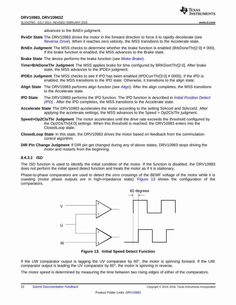
8.4.3.1 ISDThe ISD function is used to identify the initial condition of the motor. If the function is disabled, the DRV10983does not perform the initial speed detect function and treats the motor as if it is stationary.
Phase-to-phase comparators are used to detect the zero crossings of the BEMF voltage of the motor while it iscoasting (motor phase outputs are in high-impedance state). Figure 13 shows the configuration of thecomparators.
Figure 13. Initial Speed Detect Function
If the UW comparator output is lagging the UV comparator by 60°, the motor is spinning forward. If the UWcomparator output is leading the UV comparator by 60°, the motor is spinning in reverse.
The motor speed is determined by measuring the time between two rising edges of either of the comparators.

Time
Speed
Closed loop
Reverse Drive
Op2ClsThr
Open loop
RevDrThr
Coasting
23
DRV10983, DRV10983Zwww.ti.com SLVSCP6G –JULY 2014–REVISED FEBRUARY 2018
Product Folder Links: DRV10983
Submit Documentation FeedbackCopyright © 2014–2018, Texas Instruments Incorporated
If neither of the comparator outputs toggle for a given amount of time, the condition is defined as stationary. Theamount of time can be programmed by setting the register bits ISDThr[1:0].
8.4.3.2 Motor ResynchronizationThe resynchronize function works when the ISD function is enabled and determines that the initial state of themotor is spinning in the forward direction. The speed and position information measured during ISD are used toinitialize the drive state of the DRV10983, which can transition directly into the closed loop running state withoutneeding to stop the motor.
8.4.3.3 Reverse DriveThe ISD function measures the initial speed and the initial position; the DRV10983 reverse drive function acts toreverse accelerate the motor through zero speed and to continue accelerating until the closed loop threshold isreached (see Figure 14). If the reverse speed is greater than the threshold configured in RvsDrThr[1:0], then theDRV10983 waits until the motor coasts to a speed that is less than the threshold before driving the motor toreverse accelerate.
Figure 14. Reverse Drive Function
Reverse drive is suitable for applications where the load condition is light at low speed and relatively constantand where the reverse speed is low (that is, a fan motor with little friction). For other load conditions, the motorbrake function provides a method for helping force a motor which is spinning in the reverse direction to stopspinning before a normal start-up sequence.
8.4.3.4 Motor BrakeThe motor brake function can be used to stop the spinning motor before attempting to start the motor. The brakeis applied by turning on all three of the low-side driver FETs.
Brake is enabled by configuring non zero value for BrkDoneThr[2:0]. Braking is applied for time configured byBrkDoneThr[2:0] (reverse or forward). After the motor is stopped, the motor position is unknown. To proceed withrestarting in the correct direction, the IPD or Align and Go algorithm needs to be implemented. The motor startsequence is the same as it would be for a motor starting in the stationary condition.
The motor brake function can be disabled. The motor skips the brake state and attempts to spin the motor as if itwere stationary. If this happens while the motor is spinning in either direction, the start-up sequence may not besuccessful.
8.4.3.5 Motor Initialization
8.4.3.5.1 Align
The DRV10983 aligns a motor by injecting dc current through a particular phase pattern which is current flowinginto phase V, flowing out from phase W for a certain time (configured by AlignTime[2:0]). The current magnitudeis determined by OpenLCurr[1:0]. The motor should be aligned at the known position.
Clock
IPDclk
Drive
V W W V U V V U W U U W
Current
Search the Minimum Time
IPDCurrThr
Minimum Time
Permanent Magnet Position
Saturation Position of the Magnetic Field
Smallest Inductance
N
S
U V
W
24
DRV10983, DRV10983ZSLVSCP6G –JULY 2014–REVISED FEBRUARY 2018 www.ti.com
Product Folder Links: DRV10983
Submit Documentation Feedback Copyright © 2014–2018, Texas Instruments Incorporated
The time of align affects the start-up timing (see Start-Up Timing). A bigger inertial motor requires longer aligntime.
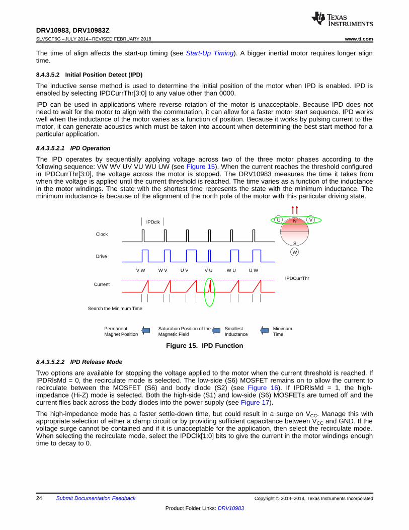
8.4.3.5.2 Initial Position Detect (IPD)
The inductive sense method is used to determine the initial position of the motor when IPD is enabled. IPD isenabled by selecting IPDCurrThr[3:0] to any value other than 0000.
IPD can be used in applications where reverse rotation of the motor is unacceptable. Because IPD does notneed to wait for the motor to align with the commutation, it can allow for a faster motor start sequence. IPD workswell when the inductance of the motor varies as a function of position. Because it works by pulsing current to themotor, it can generate acoustics which must be taken into account when determining the best start method for aparticular application.
8.4.3.5.2.1 IPD Operation
The IPD operates by sequentially applying voltage across two of the three motor phases according to thefollowing sequence: VW WV UV VU WU UW (see Figure 15). When the current reaches the threshold configuredin IPDCurrThr[3:0], the voltage across the motor is stopped. The DRV10983 measures the time it takes fromwhen the voltage is applied until the current threshold is reached. The time varies as a function of the inductancein the motor windings. The state with the shortest time represents the state with the minimum inductance. Theminimum inductance is because of the alignment of the north pole of the motor with this particular driving state.
Figure 15. IPD Function
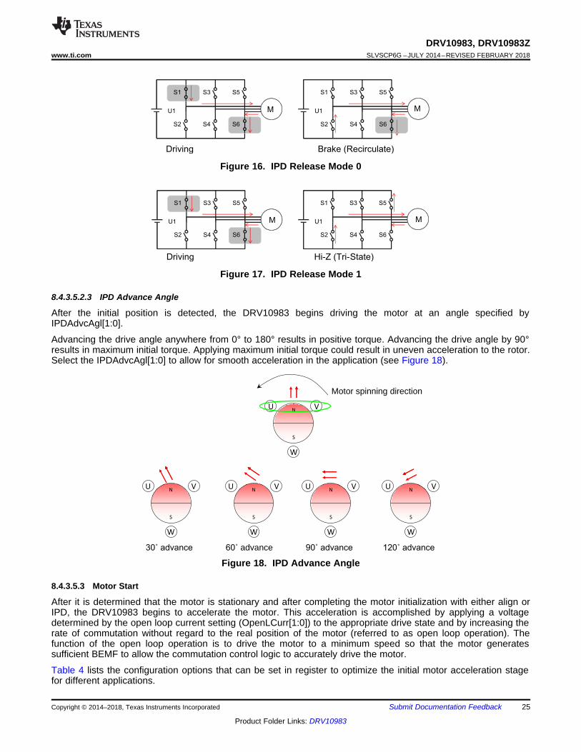
8.4.3.5.2.2 IPD Release Mode
Two options are available for stopping the voltage applied to the motor when the current threshold is reached. IfIPDRlsMd = 0, the recirculate mode is selected. The low-side (S6) MOSFET remains on to allow the current torecirculate between the MOSFET (S6) and body diode (S2) (see Figure 16). If IPDRlsMd = 1, the high-impedance (Hi-Z) mode is selected. Both the high-side (S1) and low-side (S6) MOSFETs are turned off and thecurrent flies back across the body diodes into the power supply (see Figure 17).
The high-impedance mode has a faster settle-down time, but could result in a surge on VCC. Manage this withappropriate selection of either a clamp circuit or by providing sufficient capacitance between VCC and GND. If thevoltage surge cannot be contained and if it is unacceptable for the application, then select the recirculate mode.When selecting the recirculate mode, select the IPDClk[1:0] bits to give the current in the motor windings enoughtime to decay to 0.
N
S
U V
W
Motor spinning direction
ÛDGYDQFH Ûadvance ÛDGYDQFH ÛDGYDQFH
N
S
U V
W
N
S
U V
W
N
S
U V
W
N
S
U V
W
S1
S2
U1
S3
S4
S5
S6
S1
S2
U1
S3
S4
S5
S6
Driving Hi-Z (Tri-State)
M M
Driving
S1
S2
U1
S3
S4
S5
S6
M
S1
S2
U1
S3
S4
S5
S6
Brake (Recirculate)
M
25
DRV10983, DRV10983Zwww.ti.com SLVSCP6G –JULY 2014–REVISED FEBRUARY 2018
Product Folder Links: DRV10983
Submit Documentation FeedbackCopyright © 2014–2018, Texas Instruments Incorporated
Figure 16. IPD Release Mode 0
Figure 17. IPD Release Mode 1
8.4.3.5.2.3 IPD Advance Angle
After the initial position is detected, the DRV10983 begins driving the motor at an angle specified byIPDAdvcAgl[1:0].
Advancing the drive angle anywhere from 0° to 180° results in positive torque. Advancing the drive angle by 90°results in maximum initial torque. Applying maximum initial torque could result in uneven acceleration to the rotor.Select the IPDAdvcAgl[1:0] to allow for smooth acceleration in the application (see Figure 18).
Figure 18. IPD Advance Angle
8.4.3.5.3 Motor Start
After it is determined that the motor is stationary and after completing the motor initialization with either align orIPD, the DRV10983 begins to accelerate the motor. This acceleration is accomplished by applying a voltagedetermined by the open loop current setting (OpenLCurr[1:0]) to the appropriate drive state and by increasing therate of commutation without regard to the real position of the motor (referred to as open loop operation). Thefunction of the open loop operation is to drive the motor to a minimum speed so that the motor generatessufficient BEMF to allow the commutation control logic to accurately drive the motor.
Table 4 lists the configuration options that can be set in register to optimize the initial motor acceleration stagefor different applications.

Limit LimitU I Rm Speed Hz Kt u u
Time
Speed
Close loop
Op2ClsThr
AlignTime
Accelerate Time
Accelerate Time is determined by
Op2ClsThr and A1, A2.
Speed =
t + 0.5 tA1 A2´ ´
2
26
DRV10983, DRV10983ZSLVSCP6G –JULY 2014–REVISED FEBRUARY 2018 www.ti.com
Product Folder Links: DRV10983
Submit Documentation Feedback Copyright © 2014–2018, Texas Instruments Incorporated
Table 4. Configuration Options for Controlling Open Loop Motor StartDescription Reg Name ConfigBits Min Value Max Value
Open to closed loop threshold SysOpt4 Op2ClsThr[4:0] 0.8 Hz 204.8 HzAlign time SysOpt4 AlignTime[2:0] 40 ms 5.3 sFirst order accelerate SysOpt3 StAccel[2:0] 0.3 Hz/s 76 Hz/sSecond order accelerate SysOpt3 StAccel2[2:0] 0.22 Hz/s2 57 Hz/s2Open loop current setting SysOpt2 OpenLCurr[1:0] 200 mA 1.6 AOpen loop current ramping SysOpt2 OpLCurrRt[2:0] 0.23 VCC/s 6 VCC/s
8.4.3.6 Start-Up TimingStart-up timing is determined by the align and accelerate time. The align time can be set by AlignTime[2:0], asdescribed in Register Definition . The accelerate time is defined by the open-to-closed loop thresholdOp2ClsThr[4:0] along with the first order StAccel[2:0](A1) and second order StAccel2[2:0](A2) accelerationcoefficient. Figure 19 shows the motor start-up process.
Figure 19. Motor Start-Up Process
Select the first order and second order acceleration coefficient to allow the motor to reliably accelerate from zerovelocity up to the closed loop threshold in the shortest time possible. Using a slow acceleration coefficient duringthe first order accelerate stage can help improve reliability in applications where it is difficult to accuratelyinitialize the motor with either align or IPD.
Select the open-to-closed loop threshold to allow the motor to accelerate to a speed that generates sufficientBEMF for closed loop control. This is determined by the velocity constant of the motor based on the relationshipdescribed in Equation 2.
BEMF = Kt × speed (Hz) (2)
8.4.4 Start-Up Current SettingThe start-up current setting is to control the peak start-up during open loop. During open loop operation, it isdesirable to control the magnitude of drive current applied to the motor. This is helpful in controlling andoptimizing the rate of acceleration. The limit takes effect during reverse drive, align, and acceleration.
The start current is set by programming the OpenLCurr[1:0] bits. The current should be selected to allow themotor to reliably accelerate to the handoff threshold. Heavier loads may require a higher current setting, but itshould be noted that the rate of acceleration will be limited by the acceleration rate (StAccel[2:0], StAccel2[2:0]).If the motor is started with more current than necessary to reliably reach the handoff threshold, it results in higherpower consumption.
The start current is controlled based on the relationship shown in Equation 3 and Figure 20. The duty cycleapplied to the motor is derived from the calculated value for ULimit and the magnitude of the supply voltage, VCC,as well as the drive state of the motor.
where• ILimit is configured by OpenLCurr[1:0]

BEMF = Kt × speed
Rm
V = BEMF + I× RmUM
Copyright © 2017, Texas Instruments Incorporated
27
DRV10983, DRV10983Zwww.ti.com SLVSCP6G –JULY 2014–REVISED FEBRUARY 2018
Product Folder Links: DRV10983
Submit Documentation FeedbackCopyright © 2014–2018, Texas Instruments Incorporated
• Rm is configured by Rm[6:0]• Speed is variable based open-loop acceleration profile of the motor• Kt is configured by Kt[6:0] (3)
Figure 20. Motor Start-Up Current
8.4.4.1 Start-Up Current Ramp-UpA fast change in the applied drive current may result in a sudden change in the driving torque. In someapplications, this could result in acoustic noise. To avoid this, the DRV10983 allows the option of limiting the rateat which the current is applied to the motor. OpLCurrRt[2:0] sets the maximum voltage ramp up rate that will beapplied to the motor. The waveforms in Figure 21 show how this feature can be used to gradually ramp thecurrent applied to the motor.
Start driving with fast current ramp Start driving with slow current ramp
Figure 21. Motor Startup Current Ramp
8.4.5 Closed LoopIn closed loop operation, the DRV10983 continuously samples the current in the U phase of the motor and usesthis information to estimate the BEMF voltage that is present. The drive state of the motor is controlled based onthe estimated BEMF voltage.
8.4.5.1 Half Cycle Control and Full Cycle ControlThe estimated BEMF used to control the drive state of the motor has two zero-crosses every electrical cycle. TheDRV10983 can be configured to update the drive state either once every electrical cycle or twice for everyelectrical cycle. When AdjMode is programmed to 1, half cycle adjustment is applied. The control logic istriggered at both rising edge and falling edge. When AdjMode is programmed to 0, full cycle adjustment isapplied. The control logic is triggered only at the rising edge (see Figure 22).
Half cycle adjustment provides a faster response when compared with full cycle adjustment. Use half cycleadjustment whenever the application requires operation over large dynamic loading conditions. Use the full cycleadjustment for low current (<1 A) applications because it offers more tolerance for current measurement offseterrors.

Speed
Command
Analog Input
Maximum
Speed
Command
VANA-ZS VANA-FS
Adjustment (half cycle)
Zero cross signal
Adjustment (full cycle)
Zero cross signal
Estimated PositionReal Driving Voltage
Real PositionIdeal Driving Voltage
Estimated PositionReal Driving Voltage
Real PositionIdeal Driving Voltage
28
DRV10983, DRV10983ZSLVSCP6G –JULY 2014–REVISED FEBRUARY 2018 www.ti.com
Product Folder Links: DRV10983
Submit Documentation Feedback Copyright © 2014–2018, Texas Instruments Incorporated
Figure 22. Closed Loop Control Commutation Adjustment Mode
8.4.5.2 Analog Mode Speed ControlThe SPEED input pin can be configured to operate as an analog input (SpdCtrlMd = 0).
When configured for analog mode, the voltage range on the SPEED pin can be varied from 0 to V3P3. IfSPEED > VANA_FS, the speed command is maximum. If VANA_ZS ≤ SPEED < VANA_FS the speed commandchanges linearly according to the magnitude of the voltage applied at the SPEED pin. If SPEED < VANA_ZS thespeed command is to stop the motor. Figure 23 shows the speed command when operating in analog mode.
Figure 23. Analog Mode Speed Command
8.4.5.3 Digital PWM Input Mode Speed ControlIf SpdCtrlMd = 1, the SPEED input pin is configured to operate as a PWM-encoded digital input. The PWM dutycycle applied to the SPEED pin can be varied from 0 to 100%. The speed command is proportional to the PWMinput duty cycle. The speed command stops the motor when the PWM input keeps at 0 for tEN_SL_PWM (seeFigure 24).
The frequency of the PWM input signal applied to the SPEED pin is defined as ƒPWM. This is the frequency thedevice can accept to control motor speed. It does not correspond to the PWM output frequency that is applied tothe motor phase. The PWM output frequency can be configured to be either 25 kHz when the DoubleFreq bit isset to 0 or to 50 kHz when DoubleFreq bit is set to 1.

Buffer of
SpdCtrl[8]
SpdCtrl[8]
SpdCtrl [7:0]
Write to
SpeedCtrl2
Write to
SpeedCtrl1
Speed Command
Speed
Command
PWM duty
Maximum
Speed
Command
100%0
29
DRV10983, DRV10983Zwww.ti.com SLVSCP6G –JULY 2014–REVISED FEBRUARY 2018
Product Folder Links: DRV10983
Submit Documentation FeedbackCopyright © 2014–2018, Texas Instruments Incorporated
Figure 24. PWM Mode Speed Command
8.4.5.4 I2C Mode Speed ControlThe DRV10983 can also command the speed through the I2C serial interface. To enable this feature, theOverRide bit is set to 1. When the DRV10983 is configured to operate in I2C mode, it ignores the signal appliedto the SPEED pin.
The speed command can be set by writing the SpdCtrl[8] and SpdCtrl[7:0] bits. The 9-bit SpdCtrl [8:0] located inthe SpeedCtrl1 and SpeedCntrl2 registers are used to set the peak amplitude voltage applied to the motor. Themaximum speed command is set when SpdCtrl [8:0] is set to 0x1FF (511).
When SpdCtrl [8] is written to the SpeedCtrl2 register, the data is stored, but the output is not changed. WhenSpdCtrl [7:0] is written to the SpeedCtrl1 register, the speed command is updated (see Figure 25).
Figure 25. I2C Mode Speed Control
8.4.5.5 Closed Loop AccelerateTo prevent sudden changes in the torque applied to the motor which could result in acoustic noise, theDRV10983 provides the option of limiting the maximum rate at which the speed command changes.ClsLpAccel[2:0] can be programmed to set the maximum rate at which the speed command changes (shown inFigure 26).

Phase Voltage
Phase Current
Phase BEMF tadv
Speed command
input
Speed command
after closed loop
accelerate buffer
Closed loopaccelerate settings
x%
y%
x%
y%
30
DRV10983, DRV10983ZSLVSCP6G –JULY 2014–REVISED FEBRUARY 2018 www.ti.com
Product Folder Links: DRV10983
Submit Documentation Feedback Copyright © 2014–2018, Texas Instruments Incorporated
Figure 26. Closed-Loop Accelerate
8.4.5.6 Control CoefficientThe DRV10983 continuously measures the motor current and uses this information to control the drive state ofthe motor when operating in closed loop mode. In applications where noise makes it difficult to control thecommutation optimally, the CtrlCoef[1:0] can be used to attenuate the feedback used for closed loop control. Theloop will be less reactive to the noise on the feedback and provide for a smoother output.
8.4.5.7 Commutation Control Advance AngleTo achieve the best efficiency, it is often desirable to control the drive state of the motor so that the phasecurrent of the motor is aligned with the BEMF voltage of the motor.
To align the phase current of the motor with the BEMF voltage of the motor, consider the inductive effect of themotor. The voltage applied to the motor should be applied in advance of the BEMF voltage of the motor (seeFigure 27). The DRV10983 provides configuration bits for controlling the time (tadv) between the driving voltageand BEMF.
For motors with salient pole structures, aligning the motor BEMF voltage with the motor current may not achievethe best efficiency. In these applications, the timing advance should be adjusted accordingly. Accomplish this byoperating the system at constant speed and load conditions and by adjusting the tadv until the minimum current isachieved.
Figure 27. Advance Time (tadv) Definition
The DRV10983 has two options for adjusting the motor commutate advance time. When CtrlAdvMd = 0, mode 0is selected. When CtrlAdvMd = 1, mode 1 is selected.
Mode 0: tadv is maintained to be a fixed time relative to the estimated BEMF zero cross as determined byEquation 4.
tadv = tSETTING (4)
Mode 1: tadv is maintained to be a variable time relative to the estimated BEMF zero cross as determined byEquation 5.
tadv = tSETTING × (U-BEMF)/U.
where• U is the phase voltage amplitude• BEMF is phase BEMF amplitude (5)

31
DRV10983, DRV10983Zwww.ti.com SLVSCP6G –JULY 2014–REVISED FEBRUARY 2018
Product Folder Links: DRV10983
Submit Documentation FeedbackCopyright © 2014–2018, Texas Instruments Incorporated
tSETTING (in µs) is determined by the configuration of the TCtrlAdv [6:4] and TCtrlAdv [3:0] bits as defined inEquation 6. For convenience, the available tSETTING values are provided in Table 5.
tSETTING = 2.5 µs × [TCtrlAdv[3:0]] << TCtrlAdv[6:4] (6)
Table 5. Configuring Commutation Advance Timing by Adjusting tSETTING
tSETTING (µs) TCtrlAdv[6:0] HEX tSETTING (µs) TCtrlAdv
[6:0] HEX tSETTING (µs) TCtrlAdv[6:0] HEX
0 000 0000 00 80 010 1000 28 640 101 1000 582.5 000 0001 01 90 010 1001 29 720 101 1001 595 000 0010 02 100 010 1010 2A 800 101 1010 5A
7.5 000 0011 03 110 010 1011 2B 880 101 1011 5B10 000 0100 04 120 010 1100 2C 960 101 1100 5C
12.5 000 0101 05 130 010 1101 2D 1040 101 1101 5D15 000 0110 06 140 010 1110 2E 1120 101 1110 5E
17.5 000 0111 07 150 010 1111 2F 1200 101 1111 5F20 000 1000 08 160 011 1000 38 1280 110 1000 68
22.5 000 1001 09 180 011 1001 39 1440 110 1001 6925 000 1010 0A 200 011 1010 3A 1600 110 1010 6A
27.5 000 1011 0B 220 011 1011 3B 1760 110 1011 6B30 000 1100 0C 240 011 1100 3C 1920 110 1100 6C
32.5 000 1101 0D 260 011 1101 3D 2080 110 1101 6D35 000 1110 0E 280 011 1110 3E 2240 110 1110 6E
37.5 000 1111 0F 300 011 1111 3F 2400 110 1111 6F40 001 1000 18 320 100 1000 48 2560 111 1000 7845 001 1001 19 360 100 1001 49 2880 111 1001 7950 001 1010 1A 400 100 1010 4A 3200 111 1010 7A55 001 1011 1B 440 100 1011 4B 3520 111 1011 7B60 001 1100 1C 480 100 1100 4C 3840 111 1100 7C65 001 1101 1D 520 100 1101 4D 4160 111 1101 7D70 001 1110 1E 560 100 1110 4E 4480 111 1110 7E75 001 1111 1F 600 100 1111 4F 4800 111 1111 7F
8.4.6 Current LimitThe DRV10983 has several current limit modes to help ensure optimal control of the motor and to ensure safeoperation. The various current limit modes are listed in Table 6. Acceleration current limit is used to provide ameans of controlling the amount of current delivered to the motor. This is useful when the system needs to limitthe amount of current pulled from the power supply during motor start-up. The lock detection current limit is aconfigurable threshold that can be used to limit the current applied to the motor. Overcurrent protection is used toprotect the device; therefore, it cannot be disabled or configured to a different threshold. The current limit modesare described in the following sections.
Table 6. DRV10983 Current Limit ModesCurrent Limit Mode Situation Action Fault Diagnose
Acceleration current limit Motor start Limit the output voltage amplitude No faultLock detection current limit Motor locked Stop driving the motor and enter lock state Mechanical rotation errorOvercurrent protection (OCP) Phase to phase Stop driving and recover when OC signal disappeared Circuit connection

ILIMIT
VU_LIMIT
Rm
M BEMF = Kt Speed´
Copyright © 2017, Texas Instruments Incorporated
32
DRV10983, DRV10983ZSLVSCP6G –JULY 2014–REVISED FEBRUARY 2018 www.ti.com
Product Folder Links: DRV10983
Submit Documentation Feedback Copyright © 2014–2018, Texas Instruments Incorporated
8.4.6.1 Acceleration Current LimitThe acceleration current limit limits the voltage applied to the motor to prevent the current from exceeding theprogrammed threshold. The acceleration current limit threshold is configured by writing the SWiLimitThr[3:0] bitsto select ILIMIT. The acceleration current limit does not use a direct measurement of current. It uses theprogrammed motor phase resistance, RPH_CT, and programmed BEMF constant, Kt, to limit the voltage applied tothe motor, U, as shown in Figure 28 and Equation 7.
When the acceleration current limit is active, it does not stop the motor from spinning nor does it trigger a fault.The acceleration current limit function is only available in closed loop control.
Figure 28. Acceleration Current Limit
ULIMIT = ILIMIT × RPH_CT + Speed × Kt (7)
8.4.7 Lock Detect and Fault HandlingThe DRV10983 provides several options for determining if the motor becomes locked as a result of someexternal torque. Five lock detect schemes work together to ensure the lock condition is detected quickly andreliably. Figure 29 shows the logic which integrates the various lock detect schemes. When a lock condition isdetected, the DRV10983 device takes action to prevent continuously driving the motor in order to preventdamage to the system or the motor.
In addition to detecting if there is a locked motor condition, the DRV10983 also identifies and takes action if thereis no motor connected to the system.
Each of the five lock-detect schemes and the no motor detection can be disabled by respective register bitsLockEn[5:0].
When a lock condition is detected, the MtrLck in the Status register is set. The FaultCode register provides anindication of which of the six different conditions was detected on Lock5 to Lock0. These bits are reset when themotor restarts. The bits in the FaultCode register are set even if the lock detect scheme is disabled.
The DRV10983 reacts to either locked rotor or no motor connected conditions by putting the output drivers into ahigh-impedance state. To prevent the energy in the motor from pumping the supply voltage, the DRV10983incorporates an anti-voltage-surge (AVS) process whenever the output stages transition into the high-impedancestate. The AVS function is described in AVS Function. After entering the high-impedance state as a result of afault condition, the system tries to restart after tLOCK_OFF.

DAC
+DigitalCore
–
Lock-Detection Current Limit
Speed Abnormal
Open-Loop Stuck
Closed-Loop Stuck
No-Motor Fault
LockEn(0, 1, 2, 3, 4, 5)
Hi-Z
and Restart
Logic
OR
Register:
FaultCode[5:0]
Register
Status[4]
Set
Reset
BEMF Abnormal
Copyright © 2017, Texas Instruments Incorporated
33
DRV10983, DRV10983Zwww.ti.com SLVSCP6G –JULY 2014–REVISED FEBRUARY 2018
Product Folder Links: DRV10983
Submit Documentation FeedbackCopyright © 2014–2018, Texas Instruments Incorporated
Figure 29. Lock Detect and Fault Diagnose
8.4.7.1 Lock0: Lock Detection Current Limit TriggeredThe lock detection current limit function provides a configurable threshold for limiting the current to preventdamage to the system. This is often tripped in the event of a sudden locked rotor condition. The DRV10983continuously monitors the current in the low-side drivers as shown in Figure 30. If the current goes higher thanthe threshold configured by the HWiLimitThr[2:0] bits, then the DRV10983 stops driving the motor by placing theoutput phases into a high-impedance state. The MtrLck bit is set and a lock condition is reported. It retries aftertLOCK_OFF.
Set the lock detection current limit to a higher value than the acceleration current limit.
Figure 30. Lock Detection Current Limit
8.4.7.2 Lock1: Abnormal SpeedIf motor is operating normally, the motor BEMF should always be less than output amplitude. The DRV10983uses two methods of monitoring the BEMF in the system. The U phase current is monitored to maintain anestimate of BEMF based on the setting for Rm[6:0]. In addition, the BEMF is estimated based on the operationspeed of the motor and the setting for Kt[6:0]. Figure 31 shows the method for using this information to detect alock condition. If motor BEMF is much higher than output amplitude for a certain period of time, tLCK_ETR, it meansthe estimated speed is wrong, and the motor has gotten out of phase.

Kt
Ktc
Lock detect
Kt_low
Kt_high
BEMF2 = Kt × Speed
IVU
BEMF1 = V – I× RmU
Lock Detected If BEMF2 > VU
Rm
M
Copyright © 2017, Texas Instruments Incorporated
34
DRV10983, DRV10983ZSLVSCP6G –JULY 2014–REVISED FEBRUARY 2018 www.ti.com
Product Folder Links: DRV10983
Submit Documentation Feedback Copyright © 2014–2018, Texas Instruments Incorporated
Figure 31. Lock Detection 1
8.4.7.3 Lock2: Abnormal KtFor any given motor, the integrated value of BEMF during half of an electrical cycle is constant. It is determinedby BEMF constant (Kt) (see Figure 32). It is true regardless of whether the motor is running fast or slow. Thisconstant value is continuously monitored by calculation and used as criteria to determine the motor lockcondition. It is referred to as Ktc.
Based on the Kt value programmed, create a range from Kt_low to Kt_high, if the Ktc goes beyond the range fora certain period of time, tLCK_ETR, lock is detected. Kt_low and Kt_high are determined by KtLckThr[1:0] (seeFigure 33).
Figure 32. BEMF Integration
Figure 33. Abnormal Kt Lock Detect
8.4.7.4 Lock3 (Fault3): No Motor FaultThe phase U current is checked after transitioning from open loop to closed loop. If phase U current is notgreater than 140 mA then the motor is not connected as shown in Figure 34. This condition is treated andreported as a fault.

I = 0MIN
VU
V = BEMF + I Rm = BEMFU_MIN MIN ´
Rm
M BEMF
Copyright © 2017, Texas Instruments Incorporated
DRV10983 M
35
DRV10983, DRV10983Zwww.ti.com SLVSCP6G –JULY 2014–REVISED FEBRUARY 2018
Product Folder Links: DRV10983
Submit Documentation FeedbackCopyright © 2014–2018, Texas Instruments Incorporated
Figure 34. No Motor Error
8.4.7.5 Lock4: Open Loop Motor Stuck LockLock4 is used to detect locked motor conditions while the motor start sequence is in open loop.
For a successful startup, motor speed should equal to open to closed loop handoff threshold when the motor istransitioning into closed loop. However, if the motor is locked, the motor speed is not able to match the open loopdrive rate.
If the motor BEMF is not detected for one electrical cycle after the open loop drive rate exceeds the threshold,then the open loop was unsuccessful as a result of a locked rotor condition.
8.4.7.6 Lock5: Closed Loop Motor Stuck LockIf the motor suddenly becomes locked, motor speed and Ktc are not able to be refreshed because motor BEMFzero cross may not appear after the lock. In this condition, lock can also be detected by the following scheme: ifthe current commutation period is 2× longer than the previous period.
8.4.8 AVS FunctionWhen a motor is driven, energy is transferred from the power supply into it. Some of this energy is stored in theform of inductive energy or as mechanical energy. The DRV10983 includes circuits to prevent this energy frombeing returned to the power supply which could result in pumping up the VCC voltage. This function is referred toas the AVS and acts to protect the DRV10983 as well as other circuits that share the same VCC connection. Twoforms of AVS protection are used to prevent both the mechanical energy or the inductive energy from beingreturned to the supply. Each of these modes can be independently disabled through the register configurationbits AVSMEn and AVSIndEn.
8.4.8.1 Mechanical AVS FunctionIf the speed command suddenly drops such that the BEMF voltage generated by the motor is greater than thevoltage that is applied to the motor, then the mechanical energy of the motor is returned to the power supply andthe VCC voltage surges. The mechanical AVS function works to prevent this from happening. The DRV10983buffers the speed command value and limits the resulting output voltage, UMIN, so that it is not less than theBEMF voltage of the motor. The BEMF voltage in the mechanical AVS function is determined using theprogrammed value for the Kt of the motor (Kt[6:0]) along with the speed. Figure 35 shows the criteria used by themechanical AVS function.
Figure 35. Mechanical AVS
The mechanical AVS function can operate in one of two modes, which can be configured by the register bitAVSMMd:
AVSMMd = 0 – AVS mode is always active to prevent the applied voltage from being less than the BEMFvoltage.

Motor phasedriving voltage
Fgcycle '00'
4 pole
Fgcycle '01'
6 pole
Fgcycle '10'
8 pole
Fgcycle '11'
12 pole
36
DRV10983, DRV10983ZSLVSCP6G –JULY 2014–REVISED FEBRUARY 2018 www.ti.com
Product Folder Links: DRV10983
Submit Documentation Feedback Copyright © 2014–2018, Texas Instruments Incorporated
AVSMMd = 1 – AVS mode becomes active when VCC reaches 24 V. The motor acts as a generator andreturns energy into the power supply until VCC reaches 24 V. This mode can be used to enable fasterdeceleration of the motor in applications where returning energy to the power supply is allowed.
8.4.9 PWM OutputThe DRV10983 has 16 options for PWM dead time which can be used to configure the time between one of thebridge FETs turning off and the complementary FET turning on. Deadtime[3:0] can be used to configure deadtimes between 40 ns and 640 ns. Take care that the dead time is long enough to prevent the bridge FETs fromshooting through. The recommend minimum dead time is 400 ns for 24-V VCC and 360 ns for 12-V VCC.
The DRV10983 offers two options for PWM switching frequency. When the configuration bit DoubleFreq is set to0, the output PWM frequency will be 25 kHz and when DoubleFreq is set to 1, the output PWM frequency will be50 kHz.
8.4.10 FG Customized ConfigurationThe DRV10983 provides information about the motor speed through the frequency generate (FG) pin. FG alsoprovides information about the driving state of the DRV10983.
8.4.10.1 FG Output FrequencyThe FG output frequency can be configured by FGcycle[1:0]. The default FG toggles once every electrical cycle(FGcycle = 00). Many applications configure the FG output so that it provides two pulses for every mechanicalrotation of the motor. The configuration bits provided in DRV10983 can accomplish this for 4-pole, 6-pole, 8-pole,and 12-pole motors, as shown in Figure 36.
Figure 36 shows the DRV10983 has been configured to provide FG pulses once every electrical cycle (4 pole),twice every three electrical cycle (6 pole), once every two electrical cycles (8 pole), and once every threeelectrical cycles (12 pole).
Note that when it is set to 2 FG pulses every three electrical cycles, the FG output is not 50% duty cycle. Motorspeed is able to be measured by monitoring the rising edge of the FG output.
Figure 36. FG Frequency Divider

Motor phasedriving voltage
Open loop Closed loop
FGOLsel = 00
FGOLsel = 01
Motor phasedriving voltage
Open loop Closed loop
FGOLsel = 10
Open loop Closed loop
Start-up after power on or wakeup
from sleep or standby modeRest of the startups
37
DRV10983, DRV10983Zwww.ti.com SLVSCP6G –JULY 2014–REVISED FEBRUARY 2018
Product Folder Links: DRV10983
Submit Documentation FeedbackCopyright © 2014–2018, Texas Instruments Incorporated
8.4.10.2 FG Open-Loop and Lock BehaviorNote that the FG output reflects the driving state of the motor. During normal closed loop behavior, the drivingstate and the actual state of the motor are synchronized. During open loop acceleration, however, this may notreflect the actual motor speed. During a locked motor condition, the FG output is driven high.
The DRV10983 provides three options for controlling the FG output during open loop as shown in Figure 37. Theselection of these options is determined by the FGOLsel[1:0] setting.• Option0: Open loop output FG based on driving frequency• Option1: Open loop no FG output (keep high)• Option2: FG output based on driving frequency at the first power-on start-up, and no FG output (keep high)
for any subsequent restarts
Figure 37. FG Behavior During Open Loop
8.4.11 Diagnostics and VisibilityThe DRV10983 offers extensive visibility into the motor system operation conditions stored in internal registers.This information can be monitored through the I2C interface. Information can be monitored relating to the devicestatus, motor speed, supply voltage, speed command, motor phase voltage amplitude, fault status, and others.The data is updated on the fly.
8.4.11.1 Motor Status ReadbackThe motor status register provides information on overtemperature (OverTemp), sleep or standby state(Slp_Stdby), over current (OverCurr), and locked rotor (MtrLck).

MotorSpeed[15:8]
Motor Speed Read Back
ReadMotorSpeed[7:0]
ReadMotorSpeed[15:8]
I C send out motor speed.2
MotorSpeed[7:0]
MotorSpeedBuffer[7:0]
ecycles 1 mechcycle second51 60 1530 RPM
second 2 ecycle minuteu u
38
DRV10983, DRV10983ZSLVSCP6G –JULY 2014–REVISED FEBRUARY 2018 www.ti.com
Product Folder Links: DRV10983
Submit Documentation Feedback Copyright © 2014–2018, Texas Instruments Incorporated
8.4.11.2 Motor Speed ReadbackThe motor operation speed is automatically updated in register MotorSpeed1 and MotorSpeed2 while the motoris spinning. MotorSpeed1 contains the 8 most significant bits and MotorSpeed2 contains the 8 least significantbits. The value is determined by the period for calculated BEMF zero crossings on phase U. The electrical speedof the motor is denoted as Velocity (Hz) and is calculated as shown in Equation 8.Velocity (Hz) = MotorSpeed1:MotorSpeed2 / 10 (8)
As an example consider the following:MotorSpeed1 = 0x01;MotorSpeed2 = 0xFF;Velocity = 512 (0x01FF) / 10 = 51 Hz
For a 4-pole motor, this translates to:
8.4.11.2.1 Two-Byte Register Readback
Several of the registers such as MotorSpeed report data that is contained in two registers.
To make sure that the data does not change between the reading of the first and second register reads, theDRV10983 implements a special scheme to synchronize the reading of MSB and LSB data. To ensure valid datais read when reading a two register value, use the following sequence.1. Read the MSB.2. Read the LSB.
Figure 38 shows the two-register readback circuit. When the MSB is read, the controller takes a snapshot of theLSB. The LSB data is stored in one extra register byte, which is shown as MotorSpeedBuffer[7:0]. When the LSBis read, the value of MotorSpeedBuffer[7:0] is sent.
Figure 38. Two-Byte Register Readback
8.4.11.3 Motor Electrical Period ReadbackThe motor operation electrical period is automatically updated in register MotorPeriod1 and MotorPeriod2 whilethe motor is spinning. MotorPeriod1 is the MSB and MotorPeriod2 is the LSB. The electrical period is measuredas the time between calculated BEMF zero crossings for phase U. The electrical period of the motor is denotedas d as tELE_PERIOD (µs) and is calculated as shown in Equation 9.
tELE_PERIOD (µs) = MotorPeriod1:MotorPeriod2 × 10 (9)
As an example consider the following:MotorPeriod1 = 0x01;MotorPeriod2 = 0xFF;tELE_PERIOD = 512 (0x01FF) × 10 = 5120 µs
The motor electrical period and motor speed satisfies the condition of Equation 10.tELE_PERIOD (s) × Velocity (Hz) = 1 (10)

U V
W
U V
W
N
SU V
W
U V
W
U V
W
N
S
U V
W
39
DRV10983, DRV10983Zwww.ti.com SLVSCP6G –JULY 2014–REVISED FEBRUARY 2018
Product Folder Links: DRV10983
Submit Documentation FeedbackCopyright © 2014–2018, Texas Instruments Incorporated
8.4.11.4 BEMF Constant ReadbackFor any given motor, the integrated value of BEMF during half of an electronic cycle will be constant, Ktc (seeLock2: Abnormal Kt).
The integration of the motor BEMF is processed periodically (updated every electrical cycle) while the motor isspinning. The result is stored in register MotorKt1 and MotorKt2.
The relationship is shown in Equation 11.Ktc (V/Hz)= MotorKt1:MotorKt2 / 2 /1090 (11)
8.4.11.5 Motor Estimated Position by IPDAfter inductive sense is executed the rotor position is detected within 60 electrical degrees of resolution. Theposition is stored in register IPDPosition.
The value stored in IPD Position corresponds to one of the six motor positions plus the IPD Advance Angle asshown in Table 7. For more about information about IPD, see Initial Position Detect (IPD).
Table 7. IPD Position Readback
Rotor position (°) 0 60 120 180 240 300Data1 0 43 85 128 171 213
IPD AdvanceAngle 30 60 90 120
Data2 22 44 63 85Register date (Data1 + Data2) mod (256)
8.4.11.6 Supply Voltage ReadbackThe power supply is monitored periodically during motor operation. This information is available in registerSupplyVoltage. The power supply voltage is recorded as shown in Equation 12.
VPOWERSUPPLY (V) = Supply Voltage × 30 V / 256 (12)
8.4.11.7 Speed Command ReadbackThe DRV10983 converts the various types of speed command into a speed command value (SpeedCmd) asshown in Figure 39. By reading SpeedCmd, the user can observe PWM input duty (PWM digital mode), analogvoltage (analog mode), or I2C data (I2C mode). This value is calculated as shown in Equation 13.
Equation 13 shows how the speed command as a percentage can be calculated and set in SpeedCmd.DutySPEED (%) = SpeedCmd × 100% / 255
where• DutySPEED = Speed command as a percentage• SpeedCmd = Register value (13)
8.4.11.8 Speed Command Buffer ReadbackIf acceleration current limit and AVS are enabled, the PWM duty cycle output (read back at spdCmdBuffer) maynot always match the input command (read back at SpeedCmd) shown in Figure 39. See AVS Function andCurrent Limit.
By reading the value of spdCmdBuffer, the user can observe buffered speed command (output PWM duty cycle)to the motor.

PWM in
Analog
I2C
PWM_DCO
AVS,
Acceleration Current Limit
Closed Loop Accelerate
PWM duty
ADCSpeed
Command
SpeedCmd
spdCmdBuffer
40
DRV10983, DRV10983ZSLVSCP6G –JULY 2014–REVISED FEBRUARY 2018 www.ti.com
Product Folder Links: DRV10983
Submit Documentation Feedback Copyright © 2014–2018, Texas Instruments Incorporated
Equation 14 shows how the buffered speed is calculated.DutyOUTPUT (%) = spdCmdBuffer × 100% / 255
where• DutyOUTPUT = The maximum duty cycle of the output PWM, which represents the output amplitude in
percentage.• spdCmdBuffer = Register value (14)
Figure 39. SpeedCmd and spdCmdBuffer Register
8.4.11.9 Fault DiagnosticsSee Lock Detect and Fault Handling.

41
DRV10983, DRV10983Zwww.ti.com SLVSCP6G –JULY 2014–REVISED FEBRUARY 2018
Product Folder Links: DRV10983
Submit Documentation FeedbackCopyright © 2014–2018, Texas Instruments Incorporated
(1) R/W(2) Read only(3) EEPROM
8.5 Register Maps
8.5.1 I2C Serial InterfaceThe DRV10983 provides an I2C slave interface with slave address 101 0010. TI recommends a pullup resistor4.7 kΩ to 3.3 V for I2C interface port SCL and SDA.
Four read/write registers (0x00:0x03) are used to set motor speed and control device registers and EEPROM.Device operation status can be read back through 12 read-only registers (0x10:0x1E). Another 12 EEPROMregisters (0x20:0x2B) can be accessed to program motor parameters and optimize the spin-up profile for theapplication.
8.5.2 Register Map
Register Name Address D7 D6 D5 D4 D3 D2 D1 D0SpeedCtrl1 (1) 0x00 SpdCtrl[7:0]SpeedCtrl2 (1) 0x01 OverRide SpdCtrl[8]
DevCtrl (1) 0x02 enProgKey[7:0]EECtrl (1) 0x03 sleepDis SIdata eeRefresh eeWriteStatus (2) 0x10 OverTemp Slp_Stdby OverCurr MtrLck
MotorSpeed1 (2) 0x11 MotorSpeed[15:8]MotorSpeed2 (2) 0x12 MotorSpeed[7:0]MotorPeriod1 (2) 0x13 MotorPeriod[15:8]MotorPeriod2 (2) 0x14 MotorPeriod[7:0]
MotorKt1 (2) 0x15 MotorKt[15:8]MotorKt2 (2) 0x16 MotorKt[7:0]
IPDPosition (2) 0x19 IPDPosition[7:0]SupplyVoltage (2) 0x1A SupplyVoltage [7:0]
SpeedCmd (2) 0x1B SpeedCmd [7:0]spdCmdBuffer (2) 0x1C spdCmdBuffer[7:0]
FaultCode (2) 0x1E Lock5 Lock4 Fault3 Lock2 Lock1 Lock0MotorParam1 (3) 0x20 DoubleFreq Rm[6:0]MotorParam2 (3) 0x21 AdjMode Kt[6:0]MotorParam3 (3) 0x22 CtrlAdvMd TCtrlAdv[6:0]
SysOpt1 (3) 0x23 ISDThr[1:0] IPDAdvcAgl[1:0] ISDen RvsDrEn RvsDrThr[1:0]SysOpt2 (3) 0x24 OpenLCurr[1:0] OpLCurrRt[2:0] BrkDoneThr[2:0]SysOpt3 (3) 0x25 CtrlCoef[1:0] StAccel2[2:0] StAccel[2:0]SysOpt4 (3) 0x26 Op2ClsThr[4:0] AlignTime[2:0]SysOpt5 (3) 0x27 LockEn[3:0] AVSIndEn AVSMEn AVSMMd IPDRlsMdSysOpt6 (3) 0x28 SWiLimitThr[3:0] HWiLimitThr[2:0]SysOpt7 (3) 0x29 LockEn5 ClsLpAccel[2:0] Deadtime[3:0]SysOpt8 (3) 0x2A IPDCurrThr[3:0] LockEn4 VregSel IPDClk[1:0]SysOpt9 (3) 0x2B FGOLsel[1:0] FGcycle[1:0] KtLckThr[1:0] SpdCtrlMd CLoopDis

42
DRV10983, DRV10983ZSLVSCP6G –JULY 2014–REVISED FEBRUARY 2018 www.ti.com
Product Folder Links: DRV10983
Submit Documentation Feedback Copyright © 2014–2018, Texas Instruments Incorporated
Table 8. Default EEPROMValue
Address Default Value0x20 0x4A0x21 0x4E0x22 0x2A0x23 0x000x24 0x980x25 0xE40x26 0x7A0x27 0xF40x28 0x690x29 0xB90x2A 0xAD0x2B 0x0C
(1) R/W(2) Read only
8.5.3 Register Definition
Table 9. Register DescriptionRegister
Data DescriptionName Address Bits
SpeedCtrl1 (1) 0x00 7:0 SpdCtrl[7:0]8 LSB of a 9-bit value used for the motor speed.If OverRide = 1, the user can directly control the motor speed by writing to theregister through I2C.
SpeedCtrl2 (1) 0x01
7 OverRide Use to control the SpdCtrl [8:0] bits. If OverRide = 1, the user can write the speedcommand through I2C.
6:1 N/A N/A
0 SpdCtrl [8]
MSB of a 9-bit value used for the motor speed.If OverRide = 1, user can directly control the motor speed by writing to theregister through I2C.The MSB should be written first. Digital takes a snapshot of the MSB when LSBis written.
DevCtrl (1) 0x02 7:0 enProgKey[7:0]8-bit byte use to enable programming in the EEPROM.To program the EEPROM, enProgKey = 1011 0110 (0xB6), followed immediatelyby eeWrite = 1. Otherwise, enProgKey value is reset.
EECtrl (1) 0x03
7 sleepDis Set to 1 to disable entering into sleep or standby mode.6 SIdata Set to 1 to enable the writing to the configuration registers.5 eeRefresh Copy EEPROM data to register.4 eeWrite Bit used to program (write) to the EEPROM.
3:0 N/A N/A
Status (2) 0x10
7 OverTemp Bit to indicate device temperature is over its limits.6 Slp_Stdby Bit to indicate that device went into sleep or standby mode.
5 OverCurrBit to indicate that a phase to phase overcurrent event happened. This is a stickybit, once written, it stays high even if overcurrent signal goes low. This bit iscleared on Read.
4 MtrLck Bit to indicate that the motor is locked.3 N/A N/A2 N/A N/A1 N/A N/A0 N/A N/A

43
DRV10983, DRV10983Zwww.ti.com SLVSCP6G –JULY 2014–REVISED FEBRUARY 2018
Product Folder Links: DRV10983
Submit Documentation FeedbackCopyright © 2014–2018, Texas Instruments Incorporated
Table 9. Register Description (continued)Register
Data DescriptionName Address Bits
(3) EEPROM
Motor Speed1 (2) 0x11 7:0 MotorSpeed [15:8] 16-bit value indicating the motor speed. Always read the MotorSpeed1 first.Velocity (Hz) = MotorSpeed1:MotorSpeed2 / 10For example: MotorSpeed1 = 0x01, MotorSpeed2 = 0xFF,Motor Speed = 0x01FF (511) / 10 = 51 Hz
Motor Speed2 (2) 0x12 7:0 MotorSpeed [7:0]
Motor Period1 (2) 0x13 7:0 MotorPeriod [15:8] 16-bit value indicating the motor period. Always read the MotorPeriod1 first.tELE_PERIOD (µs) = MotorPeriod1:MotorPeriod2 × 10For example: MotorPeriod1 = 0x01, MotorPeriod2 = 0xFF,Motor Period = 0x01FF (511) × 10 = 5.1 ms
Motor Period2 (2) 0x14 7:0 MotorPeriod [7:0]
MotorKt1 (2) 0x15 7:0 MotorKt[15:8] 16-bit value indicating the motor measured velocity constant. Always read theMotorKt1 first.Ktc (V/Hz)= MotorKt1:MotorKt2 / 2 /1090MotorKt1:MotorKt2 corresponding to 2 × Ktph_dig
MotorKt2 (2) 0x16 7:0 MotorKt[7:0]
IPDPosition (2) 0x19 7:0 IPDPosition [7:0] 8-bit value indicating the estimated motor position during IPD plus the IPDadvance angle (see Table 7)
SupplyVoltage (2) 0x1A 7:0 SupplyVoltage [7:0]
8-bit value indicating the supply voltageVPOWERSUPPLY (V) = SupplyVoltage[7:0] × 30 V /256For example, SupplyVoltage[7:0] = 0x67,VPOWERSUPPLY (V) = 0x67 (102) × 30 / 256 = 12 V
SpeedCmd (2) 0x1B 7:0 SpeedCmd[7:0] 8-bit value indicating the speed command based on analog or PWMin or I2C.FF indicates 100% speed command.
spdCmdBuffer (2) 0x1C 7:0 spdCmdBuffer [8:1] 8-bit value indicating the speed command after buffer output.
FF indicates 100% speed command.
FaultCode (2) 0x1E
7:6 N/A N/A5 Lock5 Stuck in closed loop4 Lock4 Stuck in open loop3 Fault3 No motor2 Lock2 Kt abnormal1 Lock1 Speed abnormal0 Lock0 Lock detection current limit
Motor Param1 (3) 0x20
7 DoubleFreq 0 = Set driver output frequency to 25 kHz1 = Set driver output frequency to 50 kHz
6:0 Rm[6:0]
Rm[6:4] : Number of the Shift bits of the motor phase resistanceRm[3:0] : Significant value of the motor phase resistanceRmdig = R_(ph_ct) / 0.00967Rmdig = Rm[3:0] ≪ Rm[6:4] See Motor Phase Resistance and Table 2
Motor Param2 (3) 0x21
7 AdjModeClosed loop adjustment mode setting0 = Full cycle adjustment1 = Half cycle adjustment
6:0 Kt[6:0]
Kt[6:4] = Number of the Shift bits of BEMF constantKt[3:0] = Significant value of the BEMF constant〖Kt〗_(ph_dig) = 1090×〖Kt〗_ph〖Kt〗_(ph_dig) = Kt[3:0] ≪ Kt[4:6]See BEMF Constant and Table 3.
Motor Param3 (3) 0x22
7 CtrlAdvMdMotor commutate control advance0 = Fixed time1 = Variable time relative to the motor speed and VCC
6:0 Tdelay[6:0]tdelay [6:4] = Number of the Shift bits of LRTIMEtdelay [3:0] = Significant value of LRTIMEtSETTING = 2.5 µs × TCtrlAdv[3:0] << TCtrlAdv[6:4]

44
DRV10983, DRV10983ZSLVSCP6G –JULY 2014–REVISED FEBRUARY 2018 www.ti.com
Product Folder Links: DRV10983
Submit Documentation Feedback Copyright © 2014–2018, Texas Instruments Incorporated
Table 9. Register Description (continued)Register
Data DescriptionName Address Bits
SysOpt1 (3) 0x23
7:6 ISDThr[1:0]
ISD stationary judgment threshold00 = 6 Hz (80 ms, no zero cross)01 = 3 Hz (160 ms, no zero cross)10 = 1.6 Hz (320 ms, no zero cross)11 = 0.8 Hz (640 ms, no zero cross)
5:4 IPDAdvcAgl [1:0]
Advancing angle after inductive sense00 = 30°01 = 60°10 = 90°11 = 120°
3 ISDen 0 = Initial speed detect (ISD) disable1 = ISD enable
2 RvsDrEn 0 = Reverse drive disable1 = Reverse drive enable
1:0 RvsDrThr[1:0]
The threshold where device starts to process reverse drive (RvsDr) or brake.00 = 6.3 Hz01 = 13 Hz10 = 26 Hz11 = 51 Hz
SysOpt2 (3) 0x24
7:6 OpenLCurr[1:0]
Open loop current setting.00 = 0.2 A01 = 0.4 A10 = 0.8 A11 = 1.6 A
5:3 OpLCurrRt:[2:0]
Open-loop current ramp-up rate setting000 = 6 VCC/s001 = 3 VCC/s010 = 1.5 VCC/s011 = 0.7 VCC/s100 = 0.34 VCC/s101 = 0.16 VCC/s110 = 0.07 VCC/s111 = 0.023 VCC/s
2:0 BrkDoneThr [2:0]
Braking mode setting000 = No brake (BrkEn = 0)001 = 2.7 s010 = 1.3 s011 = 0.67 s100 = 0.33 s101 = 0.16 s110 = 0.08 s111 = 0.04 s

45
DRV10983, DRV10983Zwww.ti.com SLVSCP6G –JULY 2014–REVISED FEBRUARY 2018
Product Folder Links: DRV10983
Submit Documentation FeedbackCopyright © 2014–2018, Texas Instruments Incorporated
Table 9. Register Description (continued)Register
Data DescriptionName Address Bits
SysOpt3 (3) 0x25
7:6 CtrlCoef[1:0]
Control coefficient00 = 0.2501 = 0.510 = 0.7511 = 1
5:3 StAccel2[2:0]
Open loop start-up accelerate (second order)000 = 57 Hz/s2
001 = 29 Hz/s2
010 = 14 Hz/s2
011 = 6.9 Hz/s2
100 = 3.3 Hz/s2
101 = 1.6 Hz/s2
110 = 0.66 Hz/s2
111 = 0.22 Hz/s2
2:0 StAccel[2:0]
Open loop start-up accelerate (first order)000 = 76 Hz/s001 = 38 Hz/s010 = 19 Hz/s011 = 9.2 Hz/s100 = 4.5 Hz/s101 = 2.1 Hz/s110 = 0.9 Hz/s111 = 0.3 Hz/s
SysOpt4 (3) 0x26
7:3 Op2ClsThr[4:0]
Open to closed loop threshold0xxxx = Range 0: n × 0.8 Hz00000 = N/A00001 = 0.8 Hz00111 = 5.6 Hz01111 = 12 Hz1xxxx = Range 1: (n + 1) × 12.8 Hz10000 = 12.8 Hz10001 = 25.6 Hz10111 = 192 Hz11111 = 204.8 Hz
2:0 AlignTime[2:0]
Align time.000 = 5.3 s001 = 2.7 s010 = 1.3 s011 = 0.67 s100 = 0.33 s101 = 0.16 s110 = 0.08 s111 = 0.04 s
SysOpt5 (3) 0x27
7 FaultEn3(LockEn[3]) No motor fault. Enabled when high
6 LockEn[2] Abnormal Kt. Enabled when high5 LockEn[1] Abnormal speed. Enabled when high4 LockEn[0] Lock detection current limit. Enabled when high3 AVSIndEn Inductive AVS enable. Enabled when high.2 AVSMEn Mechanical AVS enable. Enabled when high
1 AVSMMdMechanical AVS mode0 = AVS to VCC1 = AVS to 24 V
0 IPDRlsMdIPD release mode0 = Brake when inductive release1 = Hi-z when inductive release

46
DRV10983, DRV10983ZSLVSCP6G –JULY 2014–REVISED FEBRUARY 2018 www.ti.com
Product Folder Links: DRV10983
Submit Documentation Feedback Copyright © 2014–2018, Texas Instruments Incorporated
Table 9. Register Description (continued)Register
Data DescriptionName Address Bits
SysOpt6 (3) 0x28
7:4 SWiLimitThr [3:0]
Acceleration current limit threshold0000 = No acceleration current limit0001 = 0.2-A current limitxxxx = n × 0.2 A current limit
3:1 HWiLimitThr [2:0] Lock detection current limit threshold(n + 1) × 0.4 A
0 N/A N/A
SysOpt7 (3) 0x29
7 LockEn[5] Stuck in closed loop (no zero cross detected). Enabled when high
6:4 ClsLpAccel[2:0]
Closed loop accelerate000 = Inf fast001 = 48 VCC/s010 = 48 VCC/s011 = 0.77 VCC/s100 = 0.37 VCC/s101 = 0.19 VCC/s110 = 0.091 VCC/s111 = 0.045 VCC/s
3:0 Deadtime[3:0]
Dead time between HS and LS gate drive for motor phases0000 = 40 nsxxxx = (n + 1) × 40 ns. Recommended minimum dead time is 400 ns for 24-VVCC and 360 ns for 12-V VCC.
SysOpt8 (3) 0x2A
7:4 IPDCurrThr[3:0]
IPD (inductive sense) current threshold0000 = No IPD function. Align and Go0001 = 0.4-A current threshold.xxxx = 0.2 A × (n + 1) current threshold.
3 LockEn[4] Open loop stuck (no zero cross detected). Enabled when high
2 VregSelBuck regulator voltage select0: Vreg = 5 V1: Vreg = 3.3 V
1:0 IPDClk[1:0]
Inductive sense clock00 = 12 Hz;01 = 24 Hz;10 = 47 Hz;11 = 95 Hz
SysOpt9 (3) 0x2B
7:6 FGOLsel[1:0]
FG open loop output select00 = FG outputs in both open loop and closed loop01 = FG outputs only in closed loop10 = FG outputs closed loop and the first open loop11 = Reserved
5:4 FGcycle[1:0]
FG cycle select00 = 1 pulse output per electrical cycle01 = 2 pulses output per 3 electrical cycles10 = 1 pulse output per 2 electrical cycles11 = 1 pulse output per 3 electrical cycles
3:2 KtLckThr[1:0]
Abnormal Kt lock detect threshold00 = Kt_high = 3/2Kt. Kt_low = 3/4Kt01 = Kt_high = 2Kt. Kt_low = 3/4Kt10 = Kt_high = 3/2Kt. Kt_low = 1/2Kt11 = Kt_high = 2Kt. Kt_low = 1/2Kt
1 SpdCtrlMdSpeed input mode0 = Analog input expected at SPEED pin1 = PWM input expected at SPEED pin
0 CLoopDis 0 = Transfer to closed loop at Op2ClsThr speed1 = No transfer to closed loop. Keep in open loop

10
12Interface to
Microcontroller
1 µF
1 µF
M
1
2
3
4
5
6
7
8
9
11
24
23
22
21
20
19
18
17
16
15
14
13
VCP
CPP
CPN
SW
SWGND
VREG
V1P8
GND
V3P3
SCL
SDA
FG
VCC
VCC
W
W
V
V
U
U
PGND
PGND
DIR
SPEED
0.1 µF
0.1 µF
3.3 V or 5 V
47 µH
10 µF
10 µF
VCC
Copyright © 2016, Texas Instruments Incorporated
10
12Interface to
Microcontroller
1 µF
1 µF
M
1
2
3
4
5
6
7
8
9
11
24
23
22
21
20
19
18
17
16
15
14
13
VCP
CPP
CPN
SW
SWGND
VREG
V1P8
GND
V3P3
SCL
SDA
FG
VCC
VCC
W
W
V
V
U
U
PGND
PGND
DIR
SPEED
0.1 µF
0.1 µF
3.3 V or 5 V10 µF
10 µF
VCC
39 W
47
DRV10983, DRV10983Zwww.ti.com SLVSCP6G –JULY 2014–REVISED FEBRUARY 2018
Product Folder Links: DRV10983
Submit Documentation FeedbackCopyright © 2014–2018, Texas Instruments Incorporated
9 Application and Implementation
NOTEInformation in the following applications sections is not part of the TI componentspecification, and TI does not warrant its accuracy or completeness. TI's customers areresponsible for determining suitability of components for their purposes. Customers shouldvalidate and test their design implementation to confirm system functionality.
9.1 Application InformationThe DRV10983 is used in sensorless 3-phase BLDC motor control. The driver provides a high performance, highreliability, flexible and simple solution for appliance fan, pump, and HVAC applications. The following design inFigure 40 shows a common application of the DRV10983. For the DRV10983Z sleep mode device, a Zenerdiode must be placed in parallel with the 10-µF VREG capacitor as shown in Figure 40. The Zener diode mustmeet the requirements listed in Table 11
9.2 Typical Application
Figure 40. Typical Application Schematics for DRV10983 (Top Image) and DRV10983Z (Bottom Image)

48
DRV10983, DRV10983ZSLVSCP6G –JULY 2014–REVISED FEBRUARY 2018 www.ti.com
Product Folder Links: DRV10983
Submit Documentation Feedback Copyright © 2014–2018, Texas Instruments Incorporated
Typical Application (continued)9.2.1 Design RequirementsTable 10 provides design input parameters and motor parameters for system design.
Table 10. Recommended Application RangeMIN TYP MAX UNIT
Motor voltage 8 24 28 VBEMF constant Phase to phase, measured while motor is coasting 0.001 1.8 V/HzMotor phase resistance 1 phase, measured ph-ph and divide by 2 0.3 19 Ω
Motor electrical constant 1 phase; inductance divided by resistance, measured ph-ph is equalto 1 ph 100 5000 µs
Operating closed loopspeed Electrical frequency 1 1000 Hz
Operating current PGND, GND 0.1 2 AAbsolute maximum current During start-up or lock condition 3 A
Table 11. External ComponentsCOMPONENT PIN 1 PIN 2 RECOMMENDED
CVCC VCC GND 10-µF ceramic capacitor rated for VCC
CVCP VCP VCC 0.1-µF ceramic capacitor rated for 10 VCCP CPP CPN 0.1-µF ceramic capacitor rated for VCC × 2
LSW-VREG SW VREG 47-µH ferrite inductor with 1.15-A current rating, 1.15-A saturation current, and < 1 Ω DCresistance (buck mode)
RSW-VREG SW VREG 39-Ω series resistor rated for ¼ W (linear mode)CVREG VREG GND 10-µF ceramic capacitor rated for 10 VCV1P8 V1P8 GND 1-µF ceramic capacitor rated for 5 VCV3P3 V3P3 GND 1-µF ceramic capacitor rated for 5 VRSCL SCL V3P3 4.75-kΩ pullup to V3P3RSDA SDA V3P3 4.75-kΩ pullup to V3P3RFG FG V3P3 4.75-kΩ pullup to V3P3DZener(For 3.3-V Vregmode) GND VREG Only for DRV10983Z, Zener Voltage(Vz) = 4 V (±5%). Peak Power > 5 W, Leakage Current
<100 µADZener (For 5-V Vregmode) GND VREG Only for DRV10983Z, Zener Voltage(Vz) = 6 V (±5%). Peak Power > 5 W, Leakage Current
<100 µA
9.2.2 Detailed Design Procedure1. See the Design Requirements section and make sure your system meets the recommended application
range.2. See the DRV10983 and DRV10975 Tuning Guide and measure the motor parameters.3. See the DRV10983 and DRV10975 Tuning Guide. Configure the parameters using DRV10983 GUI, and
optimize the motor operation. The Tuning Guide takes the user through all the configurations step by step,including: start-up operation, closed-loop operation, current control, initial positioning, lock detection, andanti-voltage surge.
4. See the Programming Guide for the DRV10983 and Non-Volatile Memory section for burning tuned settingsinto EEPROM.
5. Build your hardware based on Layout Guidelines.6. Connect the device into system and validate your system solution.

FG
Phase current
Phase voltage
49
DRV10983, DRV10983Zwww.ti.com SLVSCP6G –JULY 2014–REVISED FEBRUARY 2018
Product Folder Links: DRV10983
Submit Documentation FeedbackCopyright © 2014–2018, Texas Instruments Incorporated
9.2.3 Application Curves
Figure 41. DRV10983 Start-Up Waveform Figure 42. DRV10983 Operation Current Waveform
10 Power Supply RecommendationsThe DRV10983 is designed to operate from an input voltage supply, V(VCC), range between 8 V and 28 V. Theuser must place a 10-µF ceramic capacitor rated for VCC as close as possible to the VCC and GND pins.
If the power supply ripple is more than 200 mV, in addition to the local decoupling capacitors, a bulk capacitanceis required and must be sized according to the application requirements. If the bulk capacitance is implementedin the application, the user can reduce the value of the local ceramic capacitor to 1 µF.
11 Layout
11.1 Layout Guidelines• Place VCC, GND, U, V, and W pins with thick traces because high current passes through these traces.• Place the 10-µF capacitor between VCC and GND, and as close to the VCC and GND pins as possible.• Place the capacitor between CPP and CPN, and as close to the CPP and CPN pins as possible.• Connect the GND, PGND, and SWGND under the thermal pad.• Keep the thermal pad connection as large as possible, both on the bottom side and top side. It should be one
piece of copper without any gaps.

FG
PGND
PGND
U
U
V
V
W
W
VCC
VCC
SWGND
GND
VCP
CPP
CPN
VREG
V1P8
V3P3
SCL
SDA
LSW_VREG(47 µH)
CCPP(0.1 µF)
CVREG(10 µF)
CVCP(0.1 uF)
CVCC(10 uF)
CV1P8(1 µF)
RSCL(4.75 k )W
RSDA(4.75 k )W
RFG(4.75 k )W
DIR
SPEED
SW
CV3P3(1 µF)
50
DRV10983, DRV10983ZSLVSCP6G –JULY 2014–REVISED FEBRUARY 2018 www.ti.com
Product Folder Links: DRV10983
Submit Documentation Feedback Copyright © 2014–2018, Texas Instruments Incorporated
11.2 Layout Example
Figure 43. Layout Schematic

51
DRV10983, DRV10983Zwww.ti.com SLVSCP6G –JULY 2014–REVISED FEBRUARY 2018
Product Folder Links: DRV10983
Submit Documentation FeedbackCopyright © 2014–2018, Texas Instruments Incorporated
12 Device and Documentation Support
12.1 Device Support
12.1.1 Third-Party Products DisclaimerTI'S PUBLICATION OF INFORMATION REGARDING THIRD-PARTY PRODUCTS OR SERVICES DOES NOTCONSTITUTE AN ENDORSEMENT REGARDING THE SUITABILITY OF SUCH PRODUCTS OR SERVICESOR A WARRANTY, REPRESENTATION OR ENDORSEMENT OF SUCH PRODUCTS OR SERVICES, EITHERALONE OR IN COMBINATION WITH ANY TI PRODUCT OR SERVICE.
12.2 Documentation Support
12.2.1 Related DocumentationFor related documentation see the following:• Texas Instruments, DRV10983 and DRV10975 Evaluation Module user's guide• Texas Instruments, DRV10983 and DRV10975 Tuning Guide• Texas Instruments, How to Design a Thermally-Efficient Integrated BLDC Motor Drive PCB application report• Texas Instruments, Programming Guide for the DRV10983• Texas Instruments, Speed-Control Techniques in AC-DC Operated BLDC Applications application report
12.3 TrademarksPowerPAD, E2E are trademarks of Texas Instruments.All other trademarks are the property of their respective owners.
12.4 Electrostatic Discharge CautionThese devices have limited built-in ESD protection. The leads should be shorted together or the device placed in conductive foamduring storage or handling to prevent electrostatic damage to the MOS gates.
12.5 Receiving Notification of Documentation UpdatesTo receive notification of documentation updates, navigate to the device product folder on ti.com. In the upperright corner, click on Alert me to register and receive a weekly digest of any product information that haschanged. For change details, review the revision history included in any revised document.
12.6 Community ResourcesThe following links connect to TI community resources. Linked contents are provided "AS IS" by the respectivecontributors. They do not constitute TI specifications and do not necessarily reflect TI's views; see TI's Terms ofUse.
TI E2E™ Online Community TI's Engineer-to-Engineer (E2E) Community. Created to foster collaborationamong engineers. At e2e.ti.com, you can ask questions, share knowledge, explore ideas and helpsolve problems with fellow engineers.
Design Support TI's Design Support Quickly find helpful E2E forums along with design support tools andcontact information for technical support.
12.7 GlossarySLYZ022 — TI Glossary.
This glossary lists and explains terms, acronyms, and definitions.
13 Mechanical, Packaging, and Orderable InformationThe following pages include mechanical, packaging, and orderable information. This information is the most-current data available for the designated device. This data is subject to change without notice and withoutrevision of this document. For browser-based versions of this data sheet, see the left-hand navigation pane.

PACKAGE OPTION ADDENDUM
www.ti.com 12-Jan-2018
Addendum-Page 1
PACKAGING INFORMATION
Orderable Device Status(1)
Package Type PackageDrawing
Pins PackageQty
Eco Plan(2)
Lead/Ball Finish(6)
MSL Peak Temp(3)
Op Temp (°C) Device Marking(4/5)
Samples
DRV10983PWP ACTIVE HTSSOP PWP 24 60 Green (RoHS& no Sb/Br)
CU NIPDAU Level-2-260C-1 YEAR -40 to 125 DRV10983
DRV10983PWPR ACTIVE HTSSOP PWP 24 2000 Green (RoHS& no Sb/Br)
CU NIPDAU Level-2-260C-1 YEAR -40 to 125 DRV10983
DRV10983ZPWP ACTIVE HTSSOP PWP 24 60 Green (RoHS& no Sb/Br)
CU NIPDAU Level-2-260C-1 YEAR -40 to 125 DRV10983Z
DRV10983ZPWPR ACTIVE HTSSOP PWP 24 2000 Green (RoHS& no Sb/Br)
CU NIPDAU Level-2-260C-1 YEAR -40 to 125 DRV10983Z
(1) The marketing status values are defined as follows:ACTIVE: Product device recommended for new designs.LIFEBUY: TI has announced that the device will be discontinued, and a lifetime-buy period is in effect.NRND: Not recommended for new designs. Device is in production to support existing customers, but TI does not recommend using this part in a new design.PREVIEW: Device has been announced but is not in production. Samples may or may not be available.OBSOLETE: TI has discontinued the production of the device.
(2) RoHS: TI defines "RoHS" to mean semiconductor products that are compliant with the current EU RoHS requirements for all 10 RoHS substances, including the requirement that RoHS substancedo not exceed 0.1% by weight in homogeneous materials. Where designed to be soldered at high temperatures, "RoHS" products are suitable for use in specified lead-free processes. TI mayreference these types of products as "Pb-Free".RoHS Exempt: TI defines "RoHS Exempt" to mean products that contain lead but are compliant with EU RoHS pursuant to a specific EU RoHS exemption.Green: TI defines "Green" to mean the content of Chlorine (Cl) and Bromine (Br) based flame retardants meet JS709B low halogen requirements of <=1000ppm threshold. Antimony trioxide basedflame retardants must also meet the <=1000ppm threshold requirement.
(3) MSL, Peak Temp. - The Moisture Sensitivity Level rating according to the JEDEC industry standard classifications, and peak solder temperature.
(4) There may be additional marking, which relates to the logo, the lot trace code information, or the environmental category on the device.
(5) Multiple Device Markings will be inside parentheses. Only one Device Marking contained in parentheses and separated by a "~" will appear on a device. If a line is indented then it is a continuationof the previous line and the two combined represent the entire Device Marking for that device.
(6) Lead/Ball Finish - Orderable Devices may have multiple material finish options. Finish options are separated by a vertical ruled line. Lead/Ball Finish values may wrap to two lines if the finishvalue exceeds the maximum column width.
Important Information and Disclaimer:The information provided on this page represents TI's knowledge and belief as of the date that it is provided. TI bases its knowledge and belief on informationprovided by third parties, and makes no representation or warranty as to the accuracy of such information. Efforts are underway to better integrate information from third parties. TI has taken and

PACKAGE OPTION ADDENDUM
www.ti.com 12-Jan-2018
Addendum-Page 2
continues to take reasonable steps to provide representative and accurate information but may not have conducted destructive testing or chemical analysis on incoming materials and chemicals.TI and TI suppliers consider certain information to be proprietary, and thus CAS numbers and other limited information may not be available for release.
In no event shall TI's liability arising out of such information exceed the total purchase price of the TI part(s) at issue in this document sold by TI to Customer on an annual basis.
OTHER QUALIFIED VERSIONS OF DRV10983 :
• Automotive: DRV10983-Q1
NOTE: Qualified Version Definitions:
• Automotive - Q100 devices qualified for high-reliability automotive applications targeting zero defects

TAPE AND REEL INFORMATION
*All dimensions are nominal
Device PackageType
PackageDrawing
Pins SPQ ReelDiameter
(mm)
ReelWidth
W1 (mm)
A0(mm)
B0(mm)
K0(mm)
P1(mm)
W(mm)
Pin1Quadrant
DRV10983PWPR HTSSOP PWP 24 2000 330.0 16.4 6.95 8.3 1.6 8.0 16.0 Q1
DRV10983ZPWPR HTSSOP PWP 24 2000 330.0 16.4 6.95 8.3 1.6 8.0 16.0 Q1
PACKAGE MATERIALS INFORMATION
www.ti.com 27-Jan-2018
Pack Materials-Page 1

*All dimensions are nominal
Device Package Type Package Drawing Pins SPQ Length (mm) Width (mm) Height (mm)
DRV10983PWPR HTSSOP PWP 24 2000 367.0 367.0 38.0
DRV10983ZPWPR HTSSOP PWP 24 2000 367.0 367.0 38.0
PACKAGE MATERIALS INFORMATION
www.ti.com 27-Jan-2018
Pack Materials-Page 2


IMPORTANT NOTICE
Texas Instruments Incorporated (TI) reserves the right to make corrections, enhancements, improvements and other changes to itssemiconductor products and services per JESD46, latest issue, and to discontinue any product or service per JESD48, latest issue. Buyersshould obtain the latest relevant information before placing orders and should verify that such information is current and complete.TI’s published terms of sale for semiconductor products (http://www.ti.com/sc/docs/stdterms.htm) apply to the sale of packaged integratedcircuit products that TI has qualified and released to market. Additional terms may apply to the use or sale of other types of TI products andservices.Reproduction of significant portions of TI information in TI data sheets is permissible only if reproduction is without alteration and isaccompanied by all associated warranties, conditions, limitations, and notices. TI is not responsible or liable for such reproduceddocumentation. Information of third parties may be subject to additional restrictions. Resale of TI products or services with statementsdifferent from or beyond the parameters stated by TI for that product or service voids all express and any implied warranties for theassociated TI product or service and is an unfair and deceptive business practice. TI is not responsible or liable for any such statements.Buyers and others who are developing systems that incorporate TI products (collectively, “Designers”) understand and agree that Designersremain responsible for using their independent analysis, evaluation and judgment in designing their applications and that Designers havefull and exclusive responsibility to assure the safety of Designers' applications and compliance of their applications (and of all TI productsused in or for Designers’ applications) with all applicable regulations, laws and other applicable requirements. Designer represents that, withrespect to their applications, Designer has all the necessary expertise to create and implement safeguards that (1) anticipate dangerousconsequences of failures, (2) monitor failures and their consequences, and (3) lessen the likelihood of failures that might cause harm andtake appropriate actions. Designer agrees that prior to using or distributing any applications that include TI products, Designer willthoroughly test such applications and the functionality of such TI products as used in such applications.TI’s provision of technical, application or other design advice, quality characterization, reliability data or other services or information,including, but not limited to, reference designs and materials relating to evaluation modules, (collectively, “TI Resources”) are intended toassist designers who are developing applications that incorporate TI products; by downloading, accessing or using TI Resources in anyway, Designer (individually or, if Designer is acting on behalf of a company, Designer’s company) agrees to use any particular TI Resourcesolely for this purpose and subject to the terms of this Notice.TI’s provision of TI Resources does not expand or otherwise alter TI’s applicable published warranties or warranty disclaimers for TIproducts, and no additional obligations or liabilities arise from TI providing such TI Resources. TI reserves the right to make corrections,enhancements, improvements and other changes to its TI Resources. TI has not conducted any testing other than that specificallydescribed in the published documentation for a particular TI Resource.Designer is authorized to use, copy and modify any individual TI Resource only in connection with the development of applications thatinclude the TI product(s) identified in such TI Resource. NO OTHER LICENSE, EXPRESS OR IMPLIED, BY ESTOPPEL OR OTHERWISETO ANY OTHER TI INTELLECTUAL PROPERTY RIGHT, AND NO LICENSE TO ANY TECHNOLOGY OR INTELLECTUAL PROPERTYRIGHT OF TI OR ANY THIRD PARTY IS GRANTED HEREIN, including but not limited to any patent right, copyright, mask work right, orother intellectual property right relating to any combination, machine, or process in which TI products or services are used. Informationregarding or referencing third-party products or services does not constitute a license to use such products or services, or a warranty orendorsement thereof. Use of TI Resources may require a license from a third party under the patents or other intellectual property of thethird party, or a license from TI under the patents or other intellectual property of TI.TI RESOURCES ARE PROVIDED “AS IS” AND WITH ALL FAULTS. TI DISCLAIMS ALL OTHER WARRANTIES ORREPRESENTATIONS, EXPRESS OR IMPLIED, REGARDING RESOURCES OR USE THEREOF, INCLUDING BUT NOT LIMITED TOACCURACY OR COMPLETENESS, TITLE, ANY EPIDEMIC FAILURE WARRANTY AND ANY IMPLIED WARRANTIES OFMERCHANTABILITY, FITNESS FOR A PARTICULAR PURPOSE, AND NON-INFRINGEMENT OF ANY THIRD PARTY INTELLECTUALPROPERTY RIGHTS. TI SHALL NOT BE LIABLE FOR AND SHALL NOT DEFEND OR INDEMNIFY DESIGNER AGAINST ANY CLAIM,INCLUDING BUT NOT LIMITED TO ANY INFRINGEMENT CLAIM THAT RELATES TO OR IS BASED ON ANY COMBINATION OFPRODUCTS EVEN IF DESCRIBED IN TI RESOURCES OR OTHERWISE. IN NO EVENT SHALL TI BE LIABLE FOR ANY ACTUAL,DIRECT, SPECIAL, COLLATERAL, INDIRECT, PUNITIVE, INCIDENTAL, CONSEQUENTIAL OR EXEMPLARY DAMAGES INCONNECTION WITH OR ARISING OUT OF TI RESOURCES OR USE THEREOF, AND REGARDLESS OF WHETHER TI HAS BEENADVISED OF THE POSSIBILITY OF SUCH DAMAGES.Unless TI has explicitly designated an individual product as meeting the requirements of a particular industry standard (e.g., ISO/TS 16949and ISO 26262), TI is not responsible for any failure to meet such industry standard requirements.Where TI specifically promotes products as facilitating functional safety or as compliant with industry functional safety standards, suchproducts are intended to help enable customers to design and create their own applications that meet applicable functional safety standardsand requirements. Using products in an application does not by itself establish any safety features in the application. Designers mustensure compliance with safety-related requirements and standards applicable to their applications. Designer may not use any TI products inlife-critical medical equipment unless authorized officers of the parties have executed a special contract specifically governing such use.Life-critical medical equipment is medical equipment where failure of such equipment would cause serious bodily injury or death (e.g., lifesupport, pacemakers, defibrillators, heart pumps, neurostimulators, and implantables). Such equipment includes, without limitation, allmedical devices identified by the U.S. Food and Drug Administration as Class III devices and equivalent classifications outside the U.S.TI may expressly designate certain products as completing a particular qualification (e.g., Q100, Military Grade, or Enhanced Product).Designers agree that it has the necessary expertise to select the product with the appropriate qualification designation for their applicationsand that proper product selection is at Designers’ own risk. Designers are solely responsible for compliance with all legal and regulatoryrequirements in connection with such selection.Designer will fully indemnify TI and its representatives against any damages, costs, losses, and/or liabilities arising out of Designer’s non-compliance with the terms and provisions of this Notice.
Mailing Address: Texas Instruments, Post Office Box 655303, Dallas, Texas 75265Copyright © 2018, Texas Instruments Incorporated
Related Documents