3-Phase Sensorless BLDC Motor Control Kit with S32K144 Featuring Motor Control application Tuning (MCAT) Tool by: NXP Semiconductors 1. Introduction This application note describes the design of a 3-phase Brushless DC (BLDC) motor control drive using a sensorless algorithm and 3-phase low-voltage power stage DEVKIT-MOTORGD based on SMARTMOS ® MC34GD3000 pre-driver. DEVKIT-MOTORGD is designed to supply low power 3-phase Permanent Magnet (PM) motors and measure analog and digital quantities required by this application. This design serves as an example of motor control design using NXP family of automotive motor control MCUs based on a 32-bit ARM ® Cortex ® -M4F optimized for a full range of automotive applications. Following are the supported features: • 3-phase BLDC speed control based on Six-step commutation control • Shaft position obtained by Hall sensor or by BEMF (Back Electromotive Force) voltage zero- crossing detection technique • DC-bus current, DC-bus voltage and BEMF voltage sensing • Motor speed determined by Hall sensor period or BEMF zero-crossing period • Application control user interface using FreeMASTER debugging tool NXP Semiconductors Document Number: AN12435 Application Notes Rev. 0 , 04/2019 Contents 1. Introduction........................................................................ 1 2. System concept .................................................................. 2 3. Sensorless BLDC control ................................................... 2 3.1. Overview of the brushless DC motor ...................... 2 3.2. Output voltage actuation and complementary unipolar PWM modulation technique ................................... 6 3.3. Position estimation based on BEMF zero-crossing detection................................................................................ 8 3.4. States of the sensorless BLDC control based on BEMF zero-crossing detection............................................ 15 4. Software implementation on the S32K144....................... 16 4.1. S32K144 – Key modules for BLDC six-step control16 4.2. S32K144 Device initialization .............................. 19 4.3. Software architecture ............................................ 37 5. Application Control ......................................................... 48 5.1. FreeMASTER graphical user interface ................. 48 5.2. Motor Control Application Tuning Tool ............... 49 6. Conclusion ....................................................................... 57 7. References ........................................................................ 58

Welcome message from author
This document is posted to help you gain knowledge. Please leave a comment to let me know what you think about it! Share it to your friends and learn new things together.
Transcript
3-Phase Sensorless BLDC Motor Control
Kit with S32K144
Featuring Motor Control application Tuning (MCAT) Tool
by: NXP Semiconductors
1. Introduction
This application note describes the design of a 3-phase
Brushless DC (BLDC) motor control drive using a
sensorless algorithm and 3-phase low-voltage power
stage DEVKIT-MOTORGD based on SMARTMOS®
MC34GD3000 pre-driver. DEVKIT-MOTORGD is
designed to supply low power 3-phase Permanent
Magnet (PM) motors and measure analog and digital
quantities required by this application.
This design serves as an example of motor control
design using NXP family of automotive motor control
MCUs based on a 32-bit ARM® Cortex® -M4F
optimized for a full range of automotive applications.
Following are the supported features:
• 3-phase BLDC speed control based on Six-step
commutation control
• Shaft position obtained by Hall sensor or by
BEMF (Back Electromotive Force) voltage zero-
crossing detection technique
• DC-bus current, DC-bus voltage and BEMF
voltage sensing
• Motor speed determined by Hall sensor period
or BEMF zero-crossing period
• Application control user interface using
FreeMASTER debugging tool
NXP Semiconductors Document Number: AN12435
Application Notes Rev. 0 , 04/2019
Contents
1. Introduction ........................................................................ 1 2. System concept .................................................................. 2 3. Sensorless BLDC control ................................................... 2
3.1. Overview of the brushless DC motor ...................... 2 3.2. Output voltage actuation and complementary
unipolar PWM modulation technique ................................... 6 3.3. Position estimation based on BEMF zero-crossing
detection ................................................................................ 8 3.4. States of the sensorless BLDC control based on
BEMF zero-crossing detection ............................................ 15 4. Software implementation on the S32K144....................... 16
4.1. S32K144 – Key modules for BLDC six-step control16 4.2. S32K144 Device initialization .............................. 19 4.3. Software architecture ............................................ 37
5. Application Control ......................................................... 48 5.1. FreeMASTER graphical user interface ................. 48 5.2. Motor Control Application Tuning Tool ............... 49
6. Conclusion ....................................................................... 57 7. References ........................................................................ 58
Sensorless BLDC control
3-Phase Sensorless BLDC Motor Control Kit with S32K144, Rev. 0, 04/2019
2 NXP Semiconductors
Motor Control Application Tuning (MCAT) tool
2. System concept
The system is designed to drive a 3-phase BLDC motor. The application meets the following
performance specifications:
• Targeted at the S32K144EVB Evaluation Board (refer to dedicated user manual for
S32K144EVB available at www.nxp.com). See section References for more information.
• Control technique incorporating:
o Six-step commutation control of 3-phase brushless DC motor with and without position
sensor
o Rotor position is obtained by Hall sensor or by BEMF (Back Electromotive Force)
voltage zero-crossing detection technique
o Closed-loop speed control with action period 1ms
o Bi-directional rotation
o Motor current limitation
o Alignment and start-up
o 100 μs sampling period
• Automotive Math and Motor Control Library (AMMCLIB) – Speed control loop built on blocks
of precompiled SW library (see section References)
• FreeMASTER software control interface (motor start/stop, speed setup)
• FreeMASTER software monitor
• FreeMASTER embedded Motor Control Application Tuning (MCAT) tool (motor parameters,
speed loop, sensorless parameters)
• FreeMASTER software MCAT graphical control page (required speed, actual motor speed,
start/stop status, DC-Bus voltage level, DC-Bus current, system status)
• FreeMASTER software speed scope (observes actual and desired speeds, DC-Bus voltage and
DC-Bus current)
• FreeMASTER software high-speed recorder (six-step commutation control quantities)
• DC-Bus over-voltage and under-voltage, over-current, overload and start-up fail protection.
3. Sensorless BLDC control
3.1. Overview of the brushless DC motor
The BLDC motor (Figure 1) is a rotating electric machine with a classic slotted stator filled by 3-phase
winding similar to an induction motor. The phases mounted on the stator are connected to form a star or
delta connection. The rotor has surface-mounted permanent magnets. The motor can have more than one

Sensorless BLDC control
3-Phase Sensorless BLDC Motor Control Kit with S32K144, Rev. 0, 04/2019
NXP Semiconductors 3
pole pair per phase. The number of pole pairs per phase defines the ratio between the electrical
revolution and the mechanical revolution.
The BLDC motor is equivalent to an inverted DC brushed motor, where the magnet rotates while the
conductors remain stationary. In the DC brushed motor, the commutator and brushes reverse the current
polarity in such a way that stator and rotor magnetic fields are perpendicular. However, in the brushless
DC motor, a power transistor (which must be switched in synchronization with the rotor position)
performs the polarity reversal. This process is also known as electronic commutation.
C A B
Permanent Magnets
Stator
Stator Winding
Shaft
Rotor
Air Gap
Center point
BLDC motor – cross-section
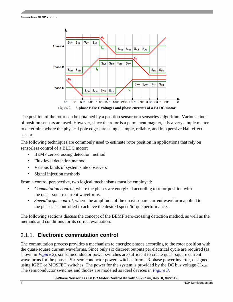
The arrangement of the magnets on the rotor creates a Trapezoidal Back Electromotive Force (BEMF)
shape when the rotor is spinning. Neglecting the higher-order harmonic terms, the BEMF in the motor
phase (ea,eb,ec) is as indicated in Figure 2. Each BEMF has a constant amplitude for 120 electrical
degrees, followed by a 60 electrical degree transition in each half-cycle. The ideal current waveforms in
each phase (ia,ib,ic) need to be quasi-square waveforms of 120 electrical degrees of conduction angle in
each half-cycle. The conduction of current in each phase must coincide with the flat part of the BEMF
waveforms, this guarantees that the developed torque is constant or ripple-free at all times. In order to
align current conduction in each phase with the flat part of the BEMF, the rotor position must be known.
Sensorless BLDC control
3-Phase Sensorless BLDC Motor Control Kit with S32K144, Rev. 0, 04/2019
4 NXP Semiconductors
3-phase BEMF voltages and phase currents of a BLDC motor
The position of the rotor can be obtained by a position sensor or a sensorless algorithm. Various kinds
of position sensors are used. However, since the rotor is a permanent magnet, it is a very simple matter
to determine where the physical pole edges are using a simple, reliable, and inexpensive Hall effect
sensor. The following techniques are commonly used to estimate rotor position in applications that rely on
sensorless control of a BLDC motor: • BEMF zero-crossing detection method • Flux level detection method • Various kinds of system state observers • Signal injection methods
From a control perspective, two logical mechanisms must be employed:
• Commutation control, where the phases are energized according to rotor position with
the quasi-square current waveforms. • Speed/torque control, where the amplitude of the quasi-square current waveform applied to
the phases is controlled to achieve the desired speed/torque performance.
The following sections discuss the concept of the BEMF zero-crossing detection method, as well as the
methods and conditions for its correct evaluation.
3.1.1. Electronic commutation control
The commutation process provides a mechanism to energize phases according to the rotor position with
the quasi-square current waveforms. Since only six discreet outputs per electrical cycle are required (as
shown in Figure 2), six semiconductor power switches are sufficient to create quasi-square current
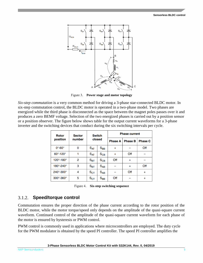
waveforms for the phases. Six semiconductor power switches form a 3-phase power inverter, designed
using IGBT or MOSFET switches. The power for the system is provided by the DC bus voltage UDCB.
The semiconductor switches and diodes are modeled as ideal devices in Figure 3.
Sensorless BLDC control
3-Phase Sensorless BLDC Motor Control Kit with S32K144, Rev. 0, 04/2019
NXP Semiconductors 5
Power stage and motor topology
Six-step commutation is a very common method for driving a 3-phase star-connected BLDC motor. In
six-step commutation control, the BLDC motor is operated in a two-phase model. Two phases are
energized while the third phase is disconnected as the space between the magnet poles passes over it and
produces a zero BEMF voltage. Selection of the two energized phases is carried out by a position sensor
or a position observer. The figure below shows table for the output current waveforms for a 3-phase
inverter and the switching devices that conduct during the six switching intervals per cycle.
Six-step switching sequence
3.1.2. Speed/torque control
Commutation ensures the proper direction of the phase current according to the rotor position of the
BLDC motor, while the motor torque/speed only depends on the amplitude of the quasi-square current
waveform. Continued control of the amplitude of the quasi-square current waveform for each phase of
the motor is ensured by hysteresis or PWM control.
PWM control is commonly used in applications where microcontrollers are employed. The duty cycle
for the PWM modulator is obtained by the speed PI controller. The speed PI controller amplifies the
Sensorless BLDC control
3-Phase Sensorless BLDC Motor Control Kit with S32K144, Rev. 0, 04/2019
6 NXP Semiconductors
error between the required and actual speeds, and its output, appropriately scaled, is assigned to the
PWM modulator.
The actual mechanical speed can be calculated as a time derivative of the shaft position mech .
Equation 1
Since the shaft travels exactly 1/6 of one electrical revolution (2 in radians) between two
commutations, the above equation can be rewritten to the following form:
5
0 60 60 120 120 180 180 240 240 300 300 360
0
360
1 1 1 360 3606elmech
nCMCM
n
d
p dt p T p T T T T T Tp T
Equation 2
Where:
• p is the number of pole pairs • TCM is the time between two consecutive commutations • TCM
n is the time between commutations in sector n = 0, 1, 2, 3, 4, 5
• el is the electrical position
3.2. Output voltage actuation and complementary unipolar PWM
modulation technique
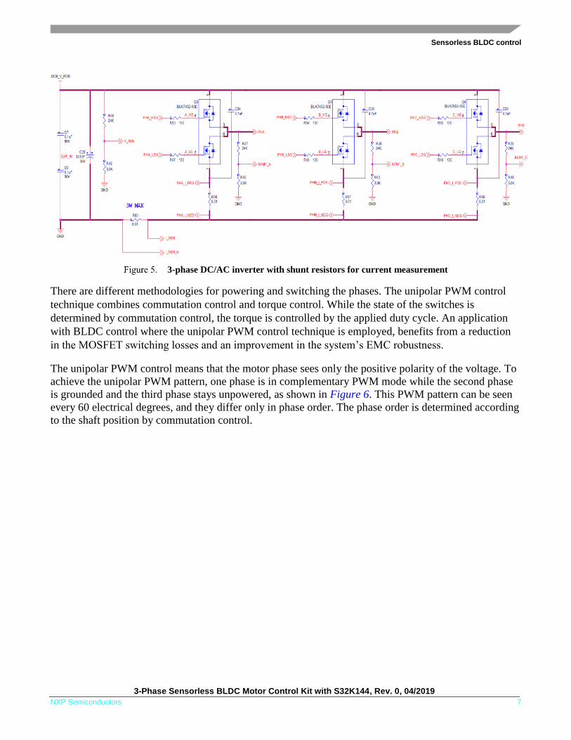
The 3-phase voltage source inverter is shown in Figure 5. Voltage dividers connected to motor phases
serve on BEMF voltage measurement. Shunt resistor R60 is used for DC Bus current measurement.
Sensorless BLDC control
3-Phase Sensorless BLDC Motor Control Kit with S32K144, Rev. 0, 04/2019
NXP Semiconductors 7
3-phase DC/AC inverter with shunt resistors for current measurement
There are different methodologies for powering and switching the phases. The unipolar PWM control
technique combines commutation control and torque control. While the state of the switches is
determined by commutation control, the torque is controlled by the applied duty cycle. An application
with BLDC control where the unipolar PWM control technique is employed, benefits from a reduction
in the MOSFET switching losses and an improvement in the system’s EMC robustness.
The unipolar PWM control means that the motor phase sees only the positive polarity of the voltage. To
achieve the unipolar PWM pattern, one phase is in complementary PWM mode while the second phase
is grounded and the third phase stays unpowered, as shown in Figure 6. This PWM pattern can be seen
every 60 electrical degrees, and they differ only in phase order. The phase order is determined according
to the shaft position by commutation control.
Sensorless BLDC control
3-Phase Sensorless BLDC Motor Control Kit with S32K144, Rev. 0, 04/2019
8 NXP Semiconductors
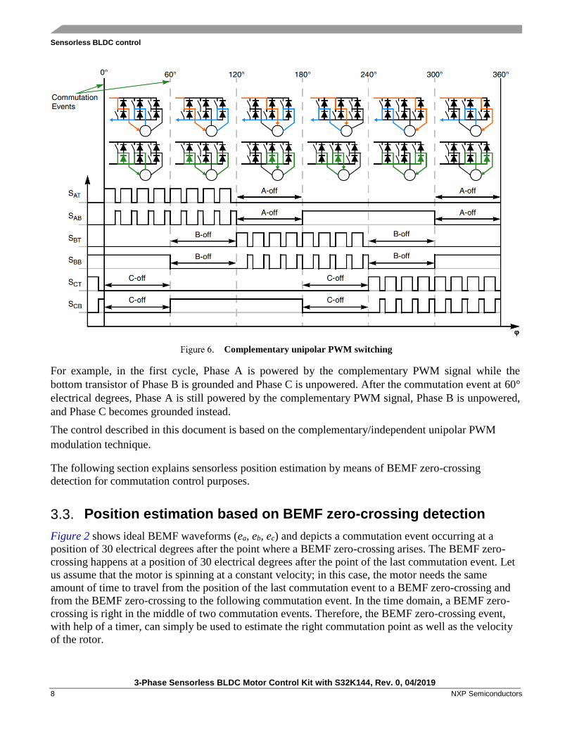
Complementary unipolar PWM switching
For example, in the first cycle, Phase A is powered by the complementary PWM signal while the
bottom transistor of Phase B is grounded and Phase C is unpowered. After the commutation event at 60°
electrical degrees, Phase A is still powered by the complementary PWM signal, Phase B is unpowered,
and Phase C becomes grounded instead.
The control described in this document is based on the complementary/independent unipolar PWM
modulation technique.
The following section explains sensorless position estimation by means of BEMF zero-crossing
detection for commutation control purposes.
3.3. Position estimation based on BEMF zero-crossing detection
Figure 2 shows ideal BEMF waveforms (ea, eb, ec) and depicts a commutation event occurring at a
position of 30 electrical degrees after the point where a BEMF zero-crossing arises. The BEMF zero-
crossing happens at a position of 30 electrical degrees after the point of the last commutation event. Let
us assume that the motor is spinning at a constant velocity; in this case, the motor needs the same
amount of time to travel from the position of the last commutation event to a BEMF zero-crossing and
from the BEMF zero-crossing to the following commutation event. In the time domain, a BEMF zero-
crossing is right in the middle of two commutation events. Therefore, the BEMF zero-crossing event,
with help of a timer, can simply be used to estimate the right commutation point as well as the velocity
of the rotor.
Sensorless BLDC control
3-Phase Sensorless BLDC Motor Control Kit with S32K144, Rev. 0, 04/2019
NXP Semiconductors 9
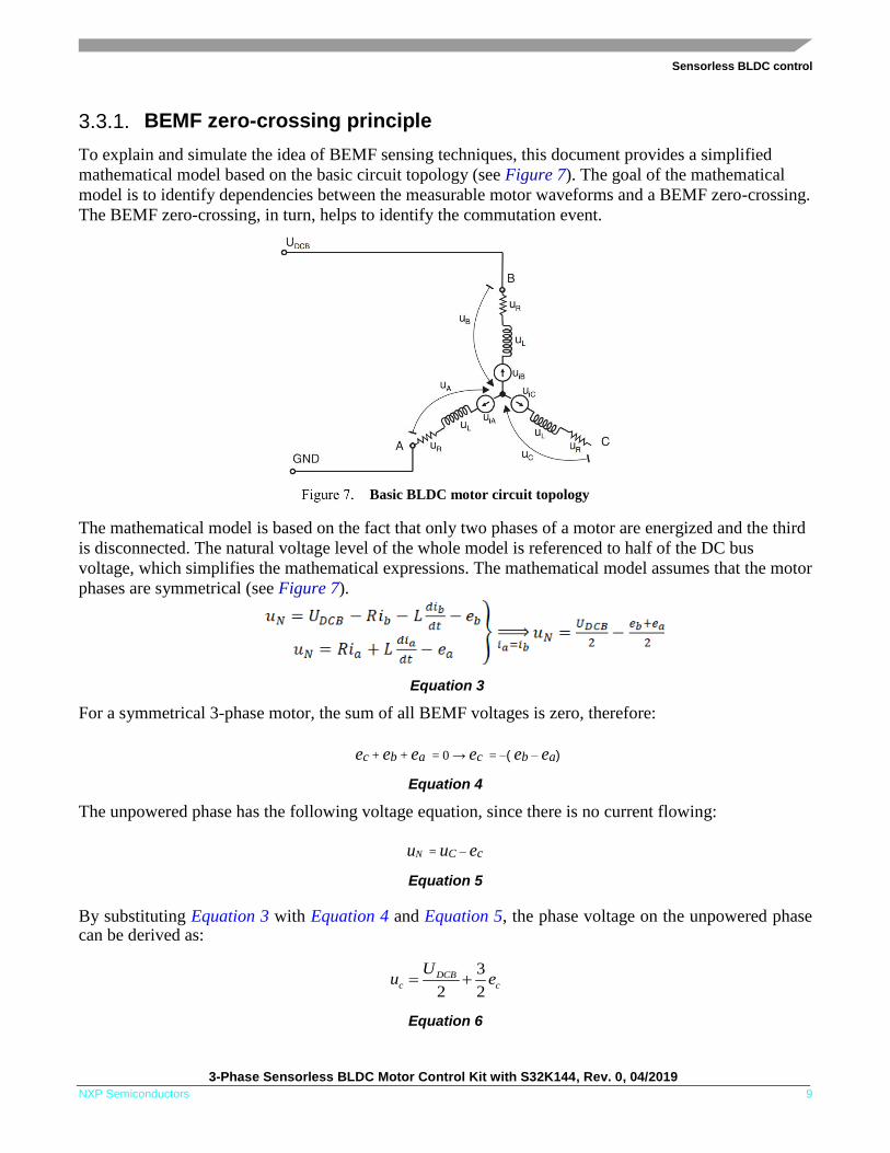
3.3.1. BEMF zero-crossing principle
To explain and simulate the idea of BEMF sensing techniques, this document provides a simplified
mathematical model based on the basic circuit topology (see Figure 7). The goal of the mathematical
model is to identify dependencies between the measurable motor waveforms and a BEMF zero-crossing.
The BEMF zero-crossing, in turn, helps to identify the commutation event.
Basic BLDC motor circuit topology
The mathematical model is based on the fact that only two phases of a motor are energized and the third
is disconnected. The natural voltage level of the whole model is referenced to half of the DC bus
voltage, which simplifies the mathematical expressions. The mathematical model assumes that the motor
phases are symmetrical (see Figure 7).
Equation 3
For a symmetrical 3-phase motor, the sum of all BEMF voltages is zero, therefore:
ec + eb + ea = 0 → ec = –( eb – ea)
Equation 4
The unpowered phase has the following voltage equation, since there is no current flowing:
uN = uC – ec
Equation 5
By substituting Equation 3 with Equation 4 and Equation 5, the phase voltage on the unpowered phase can be derived as:
3
2 2
DCBc c
Uu e
Equation 6
Sensorless BLDC control
3-Phase Sensorless BLDC Motor Control Kit with S32K144, Rev. 0, 04/2019
10 NXP Semiconductors
At the time of the BEMF zero-crossing, the BEMF voltage (ec in this case) is zero as the name implies.
Therefore, by measuring voltage at the unpowered phase (ec) and comparing it to half of the DC bus
voltage, the BEMF zero-crossing can be accurately identified.
3.3.2. BEMF zero-crossing event detection and phase current
measurement
The exact position of the rotor can be sensed by measuring the BEMF voltage induced by the
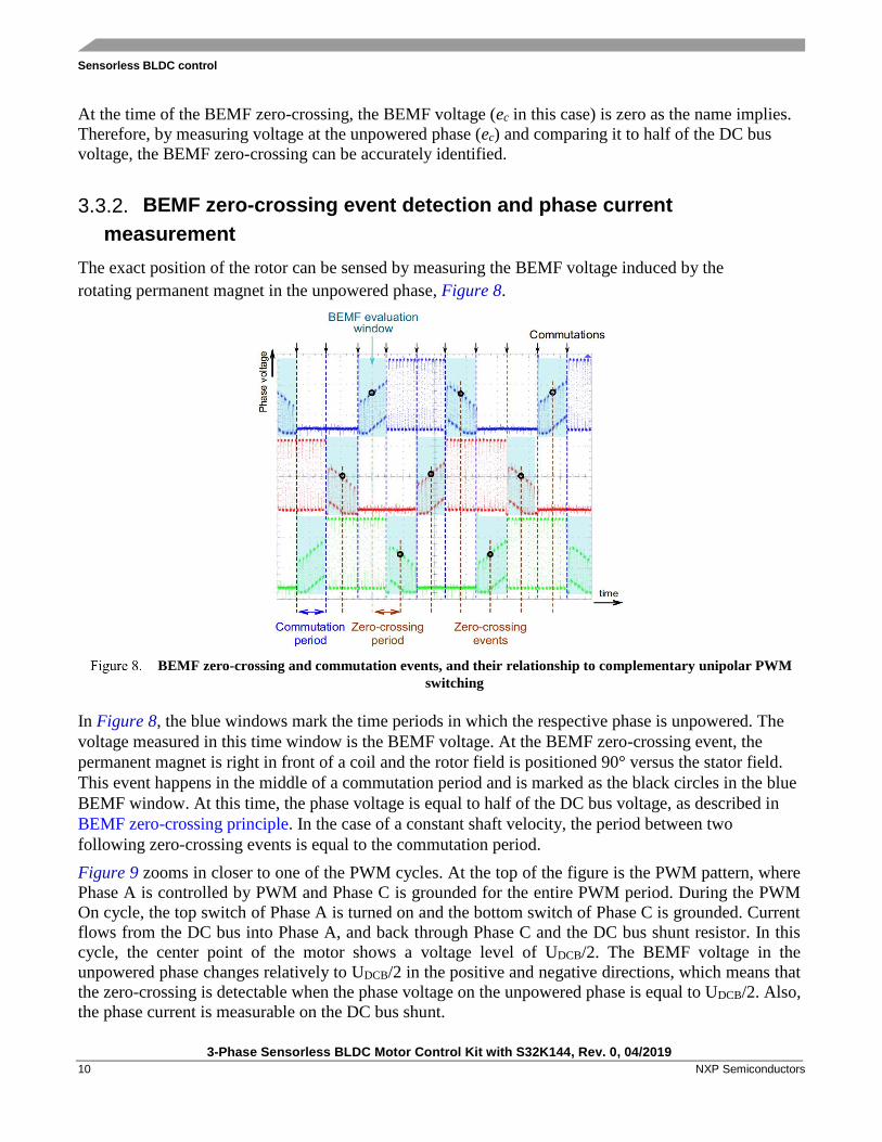
rotating permanent magnet in the unpowered phase, Figure 8.
BEMF zero-crossing and commutation events, and their relationship to complementary unipolar PWM
switching
In Figure 8, the blue windows mark the time periods in which the respective phase is unpowered. The
voltage measured in this time window is the BEMF voltage. At the BEMF zero-crossing event, the
permanent magnet is right in front of a coil and the rotor field is positioned 90° versus the stator field.
This event happens in the middle of a commutation period and is marked as the black circles in the blue
BEMF window. At this time, the phase voltage is equal to half of the DC bus voltage, as described in
BEMF zero-crossing principle. In the case of a constant shaft velocity, the period between two
following zero-crossing events is equal to the commutation period. Figure 9 zooms in closer to one of the PWM cycles. At the top of the figure is the PWM pattern, where
Phase A is controlled by PWM and Phase C is grounded for the entire PWM period. During the PWM
On cycle, the top switch of Phase A is turned on and the bottom switch of Phase C is grounded. Current
flows from the DC bus into Phase A, and back through Phase C and the DC bus shunt resistor. In this
cycle, the center point of the motor shows a voltage level of UDCB/2. The BEMF voltage in the
unpowered phase changes relatively to UDCB/2 in the positive and negative directions, which means that
the zero-crossing is detectable when the phase voltage on the unpowered phase is equal to UDCB/2. Also,
the phase current is measurable on the DC bus shunt.
Sensorless BLDC control
3-Phase Sensorless BLDC Motor Control Kit with S32K144, Rev. 0, 04/2019
NXP Semiconductors 11
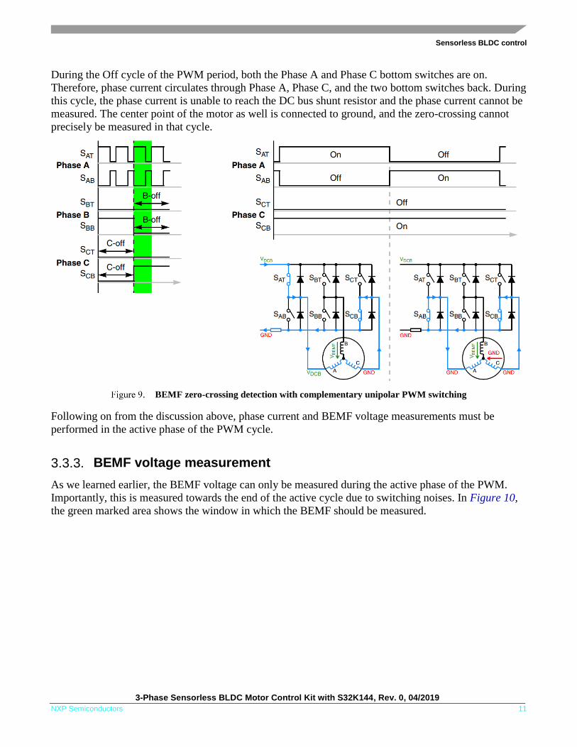
During the Off cycle of the PWM period, both the Phase A and Phase C bottom switches are on.
Therefore, phase current circulates through Phase A, Phase C, and the two bottom switches back. During
this cycle, the phase current is unable to reach the DC bus shunt resistor and the phase current cannot be
measured. The center point of the motor as well is connected to ground, and the zero-crossing cannot
precisely be measured in that cycle.
BEMF zero-crossing detection with complementary unipolar PWM switching
Following on from the discussion above, phase current and BEMF voltage measurements must be
performed in the active phase of the PWM cycle.
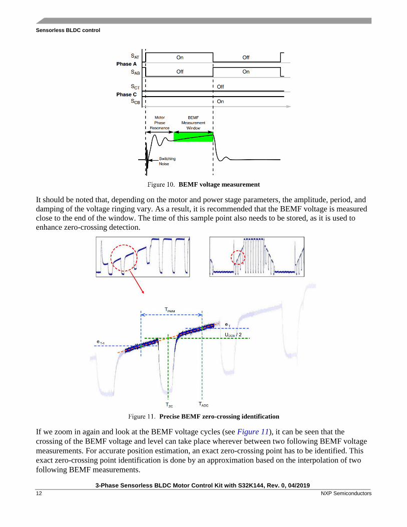
3.3.3. BEMF voltage measurement
As we learned earlier, the BEMF voltage can only be measured during the active phase of the PWM.
Importantly, this is measured towards the end of the active cycle due to switching noises. In Figure 10,
the green marked area shows the window in which the BEMF should be measured.
Sensorless BLDC control
3-Phase Sensorless BLDC Motor Control Kit with S32K144, Rev. 0, 04/2019
12 NXP Semiconductors
BEMF voltage measurement
It should be noted that, depending on the motor and power stage parameters, the amplitude, period, and
damping of the voltage ringing vary. As a result, it is recommended that the BEMF voltage is measured
close to the end of the window. The time of this sample point also needs to be stored, as it is used to
enhance zero-crossing detection.
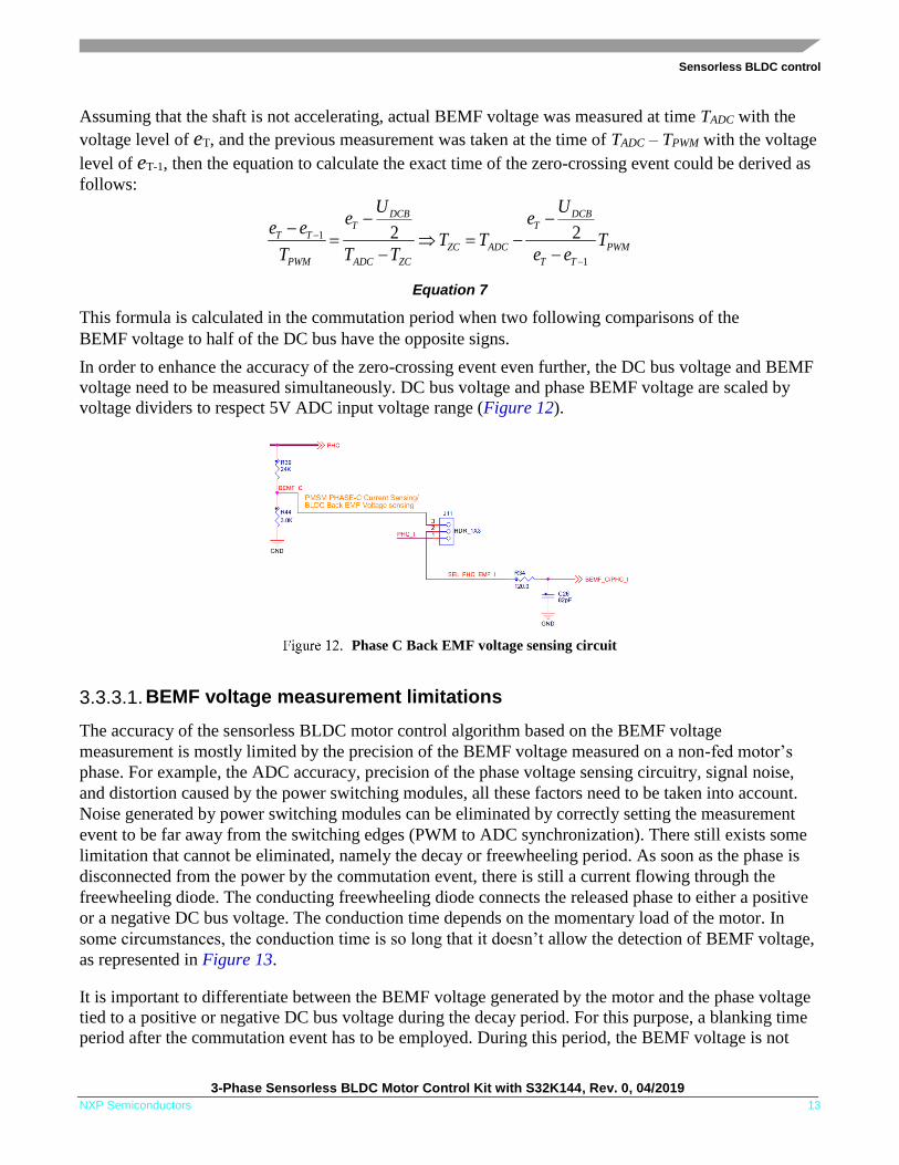
Precise BEMF zero-crossing identification
If we zoom in again and look at the BEMF voltage cycles (see Figure 11), it can be seen that the
crossing of the BEMF voltage and level can take place wherever between two following BEMF voltage
measurements. For accurate position estimation, an exact zero-crossing point has to be identified. This
exact zero-crossing point identification is done by an approximation based on the interpolation of two
following BEMF measurements.
Sensorless BLDC control
3-Phase Sensorless BLDC Motor Control Kit with S32K144, Rev. 0, 04/2019
NXP Semiconductors 13
Assuming that the shaft is not accelerating, actual BEMF voltage was measured at time TADC with the
voltage level of eT, and the previous measurement was taken at the time of TADC – TPWM with the voltage
level of eT-1, then the equation to calculate the exact time of the zero-crossing event could be derived as
follows:
1
1
2 2DCB DCB
T TT T
ZC ADC PWM
PWM ADC ZC T T
U Ue e
e eT T T
T T T e e
Equation 7
This formula is calculated in the commutation period when two following comparisons of the
BEMF voltage to half of the DC bus have the opposite signs.
In order to enhance the accuracy of the zero-crossing event even further, the DC bus voltage and BEMF
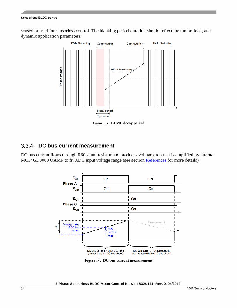
voltage need to be measured simultaneously. DC bus voltage and phase BEMF voltage are scaled by
voltage dividers to respect 5V ADC input voltage range (Figure 12).
Phase C Back EMF voltage sensing circuit
3.3.3.1. BEMF voltage measurement limitations
The accuracy of the sensorless BLDC motor control algorithm based on the BEMF voltage
measurement is mostly limited by the precision of the BEMF voltage measured on a non-fed motor’s
phase. For example, the ADC accuracy, precision of the phase voltage sensing circuitry, signal noise,
and distortion caused by the power switching modules, all these factors need to be taken into account.
Noise generated by power switching modules can be eliminated by correctly setting the measurement
event to be far away from the switching edges (PWM to ADC synchronization). There still exists some
limitation that cannot be eliminated, namely the decay or freewheeling period. As soon as the phase is
disconnected from the power by the commutation event, there is still a current flowing through the
freewheeling diode. The conducting freewheeling diode connects the released phase to either a positive
or a negative DC bus voltage. The conduction time depends on the momentary load of the motor. In
some circumstances, the conduction time is so long that it doesn’t allow the detection of BEMF voltage,
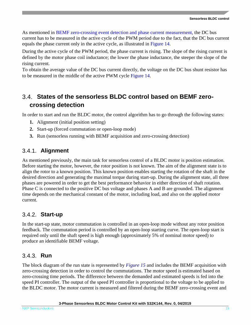
as represented in Figure 13.
It is important to differentiate between the BEMF voltage generated by the motor and the phase voltage
tied to a positive or negative DC bus voltage during the decay period. For this purpose, a blanking time
period after the commutation event has to be employed. During this period, the BEMF voltage is not
Sensorless BLDC control
3-Phase Sensorless BLDC Motor Control Kit with S32K144, Rev. 0, 04/2019
14 NXP Semiconductors
sensed or used for sensorless control. The blanking period duration should reflect the motor, load, and
dynamic application parameters.
BEMF decay period
3.3.4. DC bus current measurement
DC bus current flows through R60 shunt resistor and produces voltage drop that is amplified by internal
MC34GD3000 OAMP to fit ADC input voltage range (see section References for more details).
DC bus current measurement
Sensorless BLDC control
3-Phase Sensorless BLDC Motor Control Kit with S32K144, Rev. 0, 04/2019
NXP Semiconductors 15
As mentioned in BEMF zero-crossing event detection and phase current measurement, the DC bus
current has to be measured in the active cycle of the PWM period due to the fact, that the DC bus current
equals the phase current only in the active cycle, as illustrated in Figure 14.
During the active cycle of the PWM period, the phase current is rising. The slope of the rising current is
defined by the motor phase coil inductance; the lower the phase inductance, the steeper the slope of the
rising current.
To obtain the average value of the DC bus current directly, the voltage on the DC bus shunt resistor has
to be measured in the middle of the active PWM cycle Figure 14.
3.4. States of the sensorless BLDC control based on BEMF zero-
crossing detection
In order to start and run the BLDC motor, the control algorithm has to go through the following states:
1. Alignment (initial position setting)
2. Start-up (forced commutation or open-loop mode)
3. Run (sensorless running with BEMF acquisition and zero-crossing detection)
3.4.1. Alignment
As mentioned previously, the main task for sensorless control of a BLDC motor is position estimation.
Before starting the motor, however, the rotor position is not known. The aim of the alignment state is to
align the rotor to a known position. This known position enables starting the rotation of the shaft in the
desired direction and generating the maximal torque during start-up. During the alignment state, all three
phases are powered in order to get the best performance behavior in either direction of shaft rotation.
Phase C is connected to the positive DC bus voltage and phases A and B are grounded. The alignment
time depends on the mechanical constant of the motor, including load, and also on the applied motor
current.
3.4.2. Start-up
In the start-up state, motor commutation is controlled in an open-loop mode without any rotor position
feedback. The commutation period is controlled by an open-loop starting curve. The open-loop start is
required only until the shaft speed is high enough (approximately 5% of nominal motor speed) to
produce an identifiable BEMF voltage.
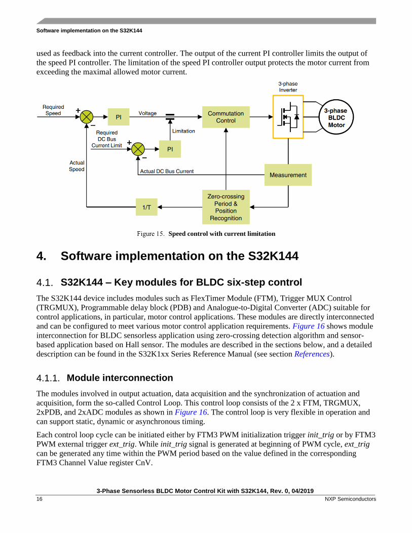
3.4.3. Run
The block diagram of the run state is represented by Figure 15 and includes the BEMF acquisition with
zero-crossing detection in order to control the commutations. The motor speed is estimated based on
zero-crossing time periods. The difference between the demanded and estimated speeds is fed into the
speed PI controller. The output of the speed PI controller is proportional to the voltage to be applied to
the BLDC motor. The motor current is measured and filtered during the BEMF zero-crossing event and
Software implementation on the S32K144
3-Phase Sensorless BLDC Motor Control Kit with S32K144, Rev. 0, 04/2019
16 NXP Semiconductors
used as feedback into the current controller. The output of the current PI controller limits the output of
the speed PI controller. The limitation of the speed PI controller output protects the motor current from
exceeding the maximal allowed motor current.
Speed control with current limitation
4. Software implementation on the S32K144
4.1. S32K144 – Key modules for BLDC six-step control
The S32K144 device includes modules such as FlexTimer Module (FTM), Trigger MUX Control
(TRGMUX), Programmable delay block (PDB) and Analogue-to-Digital Converter (ADC) suitable for
control applications, in particular, motor control applications. These modules are directly interconnected
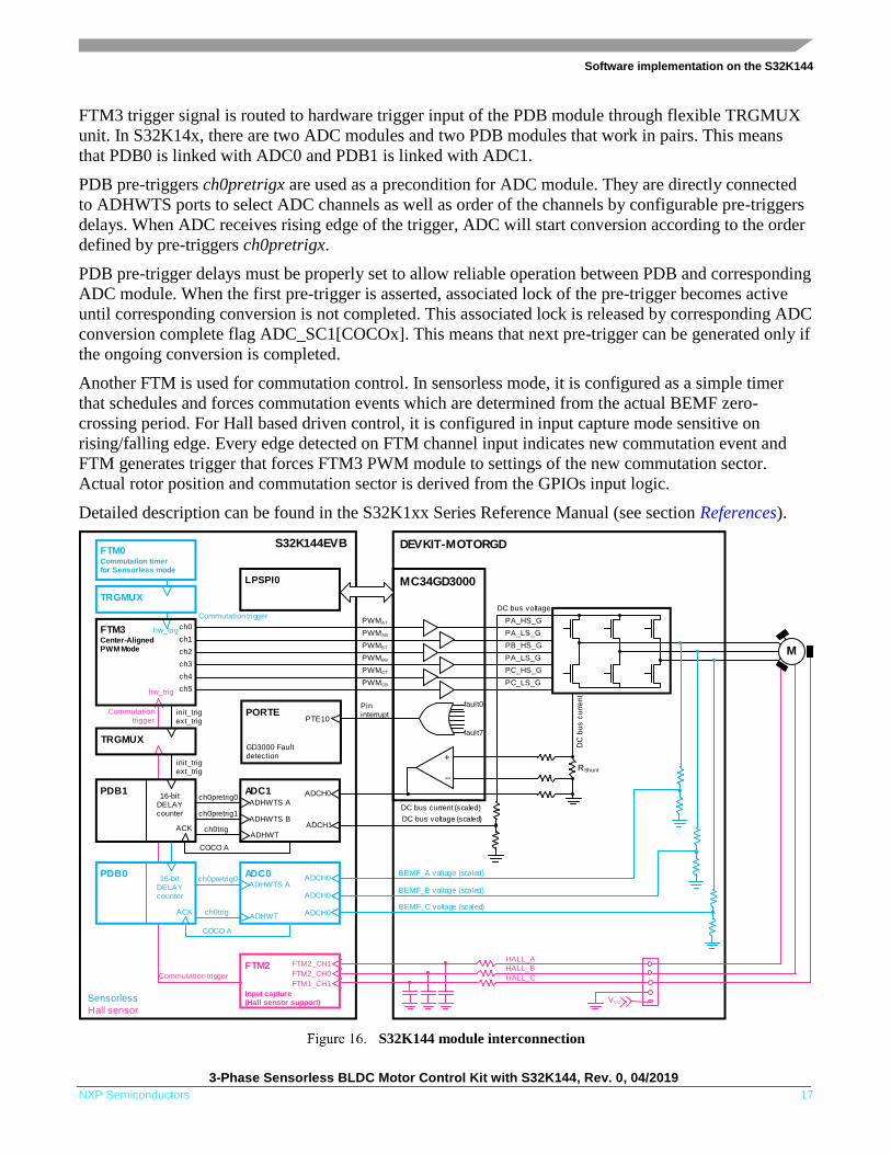
and can be configured to meet various motor control application requirements. Figure 16 shows module
interconnection for BLDC sensorless application using zero-crossing detection algorithm and sensor-
based application based on Hall sensor. The modules are described in the sections below, and a detailed
description can be found in the S32K1xx Series Reference Manual (see section References).
4.1.1. Module interconnection
The modules involved in output actuation, data acquisition and the synchronization of actuation and
acquisition, form the so-called Control Loop. This control loop consists of the 2 x FTM, TRGMUX,
2xPDB, and 2xADC modules as shown in Figure 16. The control loop is very flexible in operation and
can support static, dynamic or asynchronous timing.
Each control loop cycle can be initiated either by FTM3 PWM initialization trigger init_trig or by FTM3
PWM external trigger ext_trig. While init_trig signal is generated at beginning of PWM cycle, ext_trig
can be generated any time within the PWM period based on the value defined in the corresponding
FTM3 Channel Value register CnV.
Software implementation on the S32K144
3-Phase Sensorless BLDC Motor Control Kit with S32K144, Rev. 0, 04/2019
NXP Semiconductors 17
FTM3 trigger signal is routed to hardware trigger input of the PDB module through flexible TRGMUX
unit. In S32K14x, there are two ADC modules and two PDB modules that work in pairs. This means
that PDB0 is linked with ADC0 and PDB1 is linked with ADC1.
PDB pre-triggers ch0pretrigx are used as a precondition for ADC module. They are directly connected
to ADHWTS ports to select ADC channels as well as order of the channels by configurable pre-triggers
delays. When ADC receives rising edge of the trigger, ADC will start conversion according to the order
defined by pre-triggers ch0pretrigx.
PDB pre-trigger delays must be properly set to allow reliable operation between PDB and corresponding
ADC module. When the first pre-trigger is asserted, associated lock of the pre-trigger becomes active
until corresponding conversion is not completed. This associated lock is released by corresponding ADC
conversion complete flag ADC_SC1[COCOx]. This means that next pre-trigger can be generated only if
the ongoing conversion is completed.
Another FTM is used for commutation control. In sensorless mode, it is configured as a simple timer
that schedules and forces commutation events which are determined from the actual BEMF zero-
crossing period. For Hall based driven control, it is configured in input capture mode sensitive on
rising/falling edge. Every edge detected on FTM channel input indicates new commutation event and
FTM generates trigger that forces FTM3 PWM module to settings of the new commutation sector.
Actual rotor position and commutation sector is derived from the GPIOs input logic.
Detailed description can be found in the S32K1xx Series Reference Manual (see section References).
S32K144EVB
ADC0
ADC1
PDB0
MC34GD3000
ch5
LPSPI0
ch4
ch3
ch2
ch1
ch0PA_HS_G
PA_LS_G
PB_HS_G
PA_LS_G
PC_HS_G
PC_LS_G
PWMAT
PWMAB
PWMBT
PWMBB
PWMCT
PWMCB
16-bitDELAY counter
DC bus voltage
DEVKIT-MOTORGD
PDB116-bit
DELAY counter
ADCH0
ADCH0
ADCH0
ADCH1
RShunt
DC
bu
s c
urr
en
t
PORTEPTE10
fault0
fault7
Pin interrupt
BEMF_A voltage (scaled)
DC bus voltage (scaled)
DC bus current (scaled)
ADHWTS Ach0pretrig0
ADHWTch0trig
ch0trigADHWT
GD3000 Fault detection
init_trigext_trig
COCO A
init_trigext_trig
ACK
COCO A
ACK
+
‒
FTM2
Input capture(Hall sensor support)
FTM2_CH1
FTM2_CH0
VCC
HALL_A
HALL_B
HALL_C
ADHWTS Ach0pretrig0
ADHWTS Bch0pretrig1
ADCH0
M
FTM1_CH1Commutation trigger
hw_trig
Commutationtrigger
FTM0 Commutation timerfor Sensorless mode
hw_trig
TRGMUX
Commutation trigger
Sensorless
Hall sensor
BEMF_B voltage (scaled)
BEMF_C voltage (scaled)
FTM3 Center-Aligned PWM Mode
TRGMUX
S32K144 module interconnection
Software implementation on the S32K144
3-Phase Sensorless BLDC Motor Control Kit with S32K144, Rev. 0, 04/2019
18 NXP Semiconductors
4.1.2. S32K144 and FETs pre-driver interconnection
Excitation of power FETs is ensured by NXP MC34GD3000 pre-driver. This analog device is equipped
with charge pump that ensures external FETs drive at low power supply voltages. Moreover, three
external bootstrap capacitors provide gate charge to the high-side FETs (see section References).
Configuration of MC34GD3000 pre-driver is realized via LPSPI0 module. The MC34GD3000 allows
different operating modes to be set and locked by SPI commands. SPI commands also report condition
of the MC34GD3000 based on the internal monitoring circuits and fault detection logic. S32K144
detects fault state of the MC34GD3000 by means of interrupt signal on PTE10 pin. Integrated current
sensing amplifier with analog comparator allow to measure DC bus current and detect overcurrent.
Interconnection between S32K144 and MC34GD3000 is briefly depicted in Figure 16.
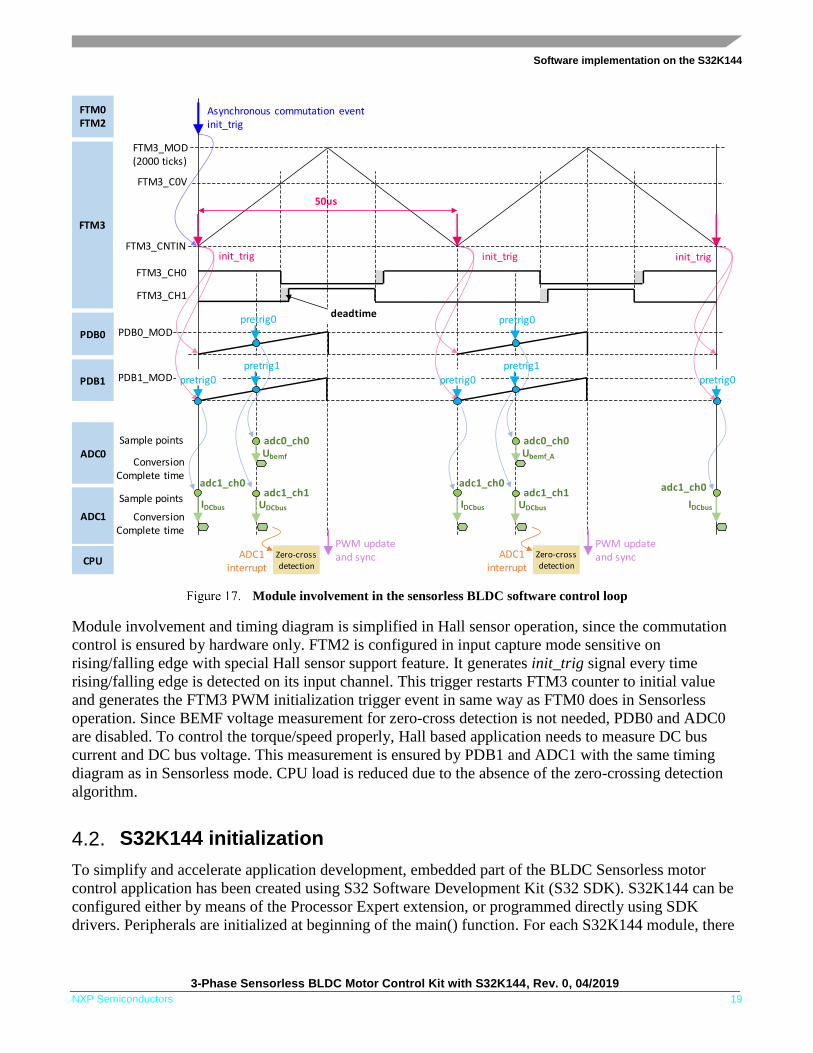
4.1.3. Module involvement in digital BLDC control loop
This section will discuss timing and modules synchronization to accomplish BLDC Six-step control on
the S32K144 and the internal hardware features. The time diagram of the automatic synchronization
between PWM and ADC in the BLDC application is shown in Figure 17.
In Sensorless mode, each commutation event gets triggered the FTM0 init_trig signal. This trigger
signal is routed to FTM3 trigger input through TRGMUX module, causing the reset of the FTM3
counter to its initial value. It also generates the FTM3 PWM initialization trigger event starting the
configurable PDB0 and PDB1 counters. ADC0 and ADC1 are triggered based on the PDB0 and PDB1
pre-trigger delays. When PDB counter reaches first pre-trigger delay value, PDB initiates first ADC
channel measurement.
DC bus current measurement is triggered first, at beginning of the PWM cycle by pretrig0. DC Bus
voltage and BEMF voltage are sampled simultaneously towards the end of the active PWM pulse. While
PDB0 triggers BEMF voltage measurement at pretrig0, DC Bus voltage measurement is triggered by
PDB1 at pretrig1. The ADC conversion results are automatically stored into a predefined queue in
memory. This sampling approach respect measurement principles of BEMF phase voltage, DC bus
current, and DC bus voltage measurement described in 3.3.3 and 3.3.4.
The ADC conversion complete interrupt notifies the CPU that the ADC conversion result values are
available for reading and further processing to identify the zero-crossing event and determine rotor
speed for speed control loop. Commutation event is then calculated based on the actual zero-crossing
period.
Software implementation on the S32K144
3-Phase Sensorless BLDC Motor Control Kit with S32K144, Rev. 0, 04/2019
NXP Semiconductors 19
FTM3_CH1
FTM3_CH0
PDB0_MOD
IDCbus UDCbus
50us
PDB1_MOD
Sample points
Sample points
ConversionComplete time
FTM3_MOD(2000 ticks)
FTM3_C0V
FTM3
PDB0
PDB1
ADC0
ConversionComplete time
ADC1
CPUADC1
interrupt
init_trigFTM3_CNTIN
Ubemf
adc1_ch0adc1_ch1
adc0_ch0
pretrig0
pretrig1
pretrig0deadtime
PWM update and sync
FTM0FTM2
Asynchronous commutation eventinit_trig
IDCbus UDCbus
Ubemf_A
adc1_ch0adc1_ch1
adc0_ch0
pretrig0
pretrig1
pretrig0
IDCbus
adc1_ch0
pretrig0
Zero-cross detection
ADC1 interrupt
PWM update and syncZero-cross
detection
init_trig init_trig
Module involvement in the sensorless BLDC software control loop
Module involvement and timing diagram is simplified in Hall sensor operation, since the commutation
control is ensured by hardware only. FTM2 is configured in input capture mode sensitive on
rising/falling edge with special Hall sensor support feature. It generates init_trig signal every time
rising/falling edge is detected on its input channel. This trigger restarts FTM3 counter to initial value
and generates the FTM3 PWM initialization trigger event in same way as FTM0 does in Sensorless
operation. Since BEMF voltage measurement for zero-cross detection is not needed, PDB0 and ADC0
are disabled. To control the torque/speed properly, Hall based application needs to measure DC bus
current and DC bus voltage. This measurement is ensured by PDB1 and ADC1 with the same timing
diagram as in Sensorless mode. CPU load is reduced due to the absence of the zero-crossing detection
algorithm.
4.2. S32K144 initialization
To simplify and accelerate application development, embedded part of the BLDC Sensorless motor
control application has been created using S32 Software Development Kit (S32 SDK). S32K144 can be
configured either by means of the Processor Expert extension, or programmed directly using SDK
drivers. Peripherals are initialized at beginning of the main() function. For each S32K144 module, there
Software implementation on the S32K144
3-Phase Sensorless BLDC Motor Control Kit with S32K144, Rev. 0, 04/2019
20 NXP Semiconductors
is a specific configuration function that uses S32 SDK APIs and configuration structures generated by
PEx to configure the MCU.
• McuClockConfig() – MCU clock configuration
• McuPowerConfig() – MCU power management configuration
• McuTrigmuxConfig() – TRGMUX module configuration
• McuPinsConfig() – PINs and PORT modules configuration
• McuLpuartConfig() – LPUART module configuration
• McuLpitConfig() – LPIT module configuration
• McuAdcConfig() – ADC modules configuration
• McuPdbConfig() – PDB modules configuration
• McuFtmConfig() – FTM modules configuration
Detailed SDK documentation can be found in folder created with S32 Design Studio installation.
(References).
4.2.1. Clock configuration and power management
S32K144 features a complex clocking sourcing, distribution and power management. To run a core of
the S32K144 as well as some MCU peripherals at maximum frequency 80 MHz in normal RUN mode,
S32K144 is supplied externally by 8 MHz crystal. This clock source supplies Phase-lock-loop (PLL),
which circuit multiplies frequency by 40 and divides by 2 resulting 160 MHz frequency on output. PLL
output is then divided by 2 to supply core and system (80 MHz), further divided by two and three to
supply bus clock (40 MHz) and flash clock (26.67 MHz), respectively. This clock configuration belongs
to one of the typical and recommended. It is summarized in Table 1.
Table 1. S32K144 clock configuration in RUN mode
Clock Frequency
CORE_CLOCK 80 MHz
SYS_CLK 80 MHz
BUS_CLK 40MHz
FLASH_CLK 26.67MHz (max freq. in RUN
mode)
This clock configuration and power management can be setup easily by S32 Processor Expert. Preview
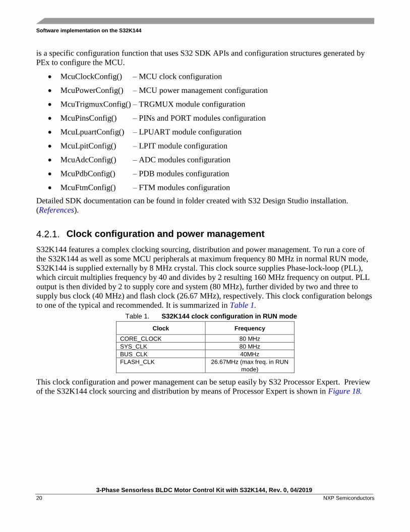
of the S32K144 clock sourcing and distribution by means of Processor Expert is shown in Figure 18.
Software implementation on the S32K144
3-Phase Sensorless BLDC Motor Control Kit with S32K144, Rev. 0, 04/2019
NXP Semiconductors 21
S32K144 clock configuration in Processor Expert
Once the clock configuration is set, Processor Expert generates static configuration structure
clockMan1_InitConfig0, that is called by SDK’s CLOCK_SYS_Init function through array of the
configuration pointers g_clockManConfigsArr, Example 1.
Example 1. S32K144 clock configuration controlled by S32 SDK void McuClockConfig(void)
{
/* Clock configuration for MCU and MCU's peripherals */
CLOCK_SYS_Init(g_clockManConfigsArr,
CLOCK_MANAGER_CONFIG_CNT,
g_clockManCallbacksArr,
CLOCK_MANAGER_CALLBACK_CNT);
/* Clock configuration update */
CLOCK_SYS_UpdateConfiguration(0, CLOCK_MANAGER_POLICY_FORCIBLE);
}
...
/*! @brief Array of pointers to User configuration structures */ clock_manager_user_config_t const * g_clockManConfigsArr[] = { &clockMan1_InitConfig0 }; /*! @brief Array of pointers to User defined Callbacks configuration structures */ clock_manager_callback_user_config_t * g_clockManCallbacksArr[] = {(void*)0}; /* END clockMan1. */
As it was discussed at begging of this section, power management of the S32K144 is configured for
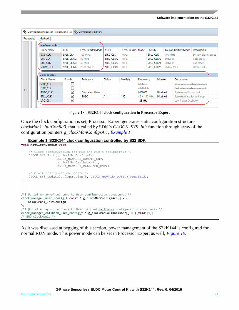
normal RUN mode. This power mode can be set in Processor Expert as well, Figure 19.
Software implementation on the S32K144
3-Phase Sensorless BLDC Motor Control Kit with S32K144, Rev. 0, 04/2019
22 NXP Semiconductors
S32K144 power management configuration in Processor Expert
Static configuration generated by Processor Expert is called by SDK’s POWER_SYS_Init function to
update power mode of the S32K144 device, Example 2.
Example 2. S32K144 power management controlled by S32 SDK void McuPowerConfig(void) { /* Power mode configuration for RUN mode */ POWER_SYS_Init(&powerConfigsArr, 0, &powerStaticCallbacksConfigsArr,0); /* Power mode configuration update */ POWER_SYS_SetMode(0,POWER_MANAGER_POLICY_AGREEMENT); } ...
/*! @brief User Configuration structure power_managerCfg_0 */ power_manager_user_config_t pwrMan1_InitConfig0 = { .powerMode = POWER_MANAGER_RUN, /*!< Power manager mode */ .sleepOnExitValue = false, /*!< Sleep on exit value */ }; /*! @brief Array of pointers to User configuration structures */ power_manager_user_config_t * powerConfigsArr[] = { &pwrMan1_InitConfig0 }; /*! @brief Array of pointers to User defined Callbacks configuration structures */
Same mechanism between Processor Expert and S32 SDK works for all S32K144 peripherals, which are
discussed below.
4.2.2. FlexTimer Module (FTM)
FlexTimer module (FTM) is built upon a timer with a 16-bit counter. It contains an extended set of features
that meet the demands of motor control, including the signed up-counter, dead time insertion hardware, fault
control inputs, enhanced triggering functionality, and initialization and polarity control.
Software implementation on the S32K144
3-Phase Sensorless BLDC Motor Control Kit with S32K144, Rev. 0, 04/2019
NXP Semiconductors 23
4.2.2.1. Center-aligned PWM mode
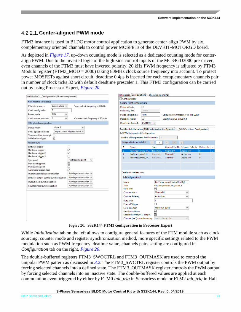
FTM3 instance is used in BLDC motor control application to generate center-align PWM by six,
complementary oriented channels to control power MOSFETs of the DEVKIT-MOTORGD board.
As depicted in Figure 17, up-down counting mode is selected as a dedicated counting mode for center-
align PWM. Due to the inverted logic of the high-side control inputs of the MC34GD3000 pre-driver,
even channels of the FTM3 must have inverted polarity. 20 kHz PWM frequency is adjusted by FTM3
Modulo register (FTM3_MOD = 2000) taking 80MHz clock source frequency into account. To protect
power MOSFETs against short circuit, deadtime 0.4μs is inserted for each complementary channels pair
in number of clock ticks 32 with default deadtime prescaler 1. This FTM3 configuration can be carried
out by using Processor Expert, Figure 20.
S32K144 FTM3 configuration in Processor Expert
While Initialization tab on the left allows to configure general features of the FTM module such as clock
sourcing, counter mode and register synchronization method, more specific settings related to the PWM
modulation such as PWM frequency, deatime value, channels pairs setting are configured in
Configuration tab on the right, Figure 20.
The double-buffered registers FTM3_SWOCTRL and FTM3_OUTMASK are used to control the
unipolar PWM pattern as discussed in 3.2. The FTM3_SWCTRL register controls the PWM output by
forcing selected channels into a defined state. The FTM3_OUTMASK register controls the PWM output
by forcing selected channels into an inactive state. The double-buffered values are applied at each
commutation event triggered by either by FTM0 init_trig in Sensorless mode or FTM2 init_trig in Hall
Software implementation on the S32K144
3-Phase Sensorless BLDC Motor Control Kit with S32K144, Rev. 0, 04/2019
24 NXP Semiconductors
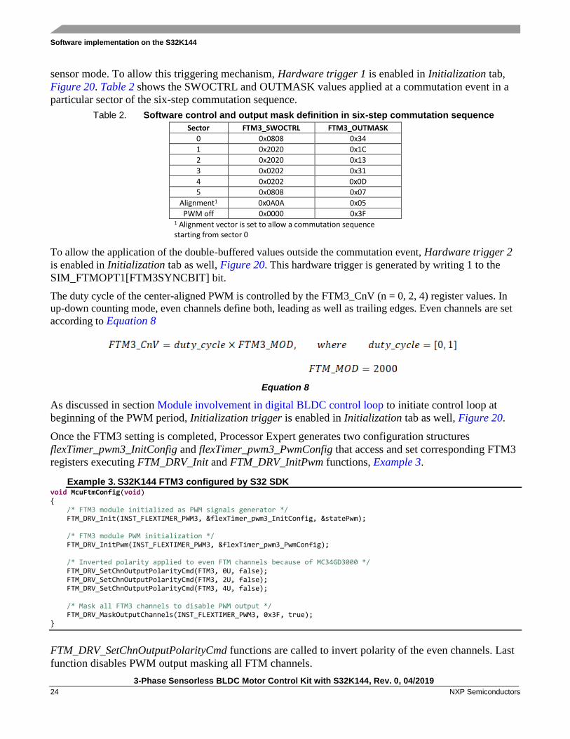
sensor mode. To allow this triggering mechanism, Hardware trigger 1 is enabled in Initialization tab,
Figure 20. Table 2 shows the SWOCTRL and OUTMASK values applied at a commutation event in a
particular sector of the six-step commutation sequence.
Table 2. Software control and output mask definition in six-step commutation sequence
Sector FTM3_SWOCTRL FTM3_OUTMASK
0 0x0808 0x34
1 0x2020 0x1C
2 0x2020 0x13
3 0x0202 0x31
4 0x0202 0x0D
5 0x0808 0x07
Alignment1 0x0A0A 0x05
PWM off 0x0000 0x3F 1 Alignment vector is set to allow a commutation sequence starting from sector 0
To allow the application of the double-buffered values outside the commutation event, Hardware trigger 2
is enabled in Initialization tab as well, Figure 20. This hardware trigger is generated by writing 1 to the
SIM_FTMOPT1[FTM3SYNCBIT] bit.
The duty cycle of the center-aligned PWM is controlled by the FTM3_CnV (n = 0, 2, 4) register values. In
up-down counting mode, even channels define both, leading as well as trailing edges. Even channels are set
according to Equation 8
Equation 8
As discussed in section Module involvement in digital BLDC control loop to initiate control loop at
beginning of the PWM period, Initialization trigger is enabled in Initialization tab as well, Figure 20.
Once the FTM3 setting is completed, Processor Expert generates two configuration structures
flexTimer_pwm3_InitConfig and flexTimer_pwm3_PwmConfig that access and set corresponding FTM3
registers executing FTM_DRV_Init and FTM_DRV_InitPwm functions, Example 3.
Example 3. S32K144 FTM3 configured by S32 SDK void McuFtmConfig(void) { /* FTM3 module initialized as PWM signals generator */ FTM_DRV_Init(INST_FLEXTIMER_PWM3, &flexTimer_pwm3_InitConfig, &statePwm); /* FTM3 module PWM initialization */ FTM_DRV_InitPwm(INST_FLEXTIMER_PWM3, &flexTimer_pwm3_PwmConfig); /* Inverted polarity applied to even FTM channels because of MC34GD3000 */ FTM_DRV_SetChnOutputPolarityCmd(FTM3, 0U, false); FTM_DRV_SetChnOutputPolarityCmd(FTM3, 2U, false); FTM_DRV_SetChnOutputPolarityCmd(FTM3, 4U, false); /* Mask all FTM3 channels to disable PWM output */ FTM_DRV_MaskOutputChannels(INST_FLEXTIMER_PWM3, 0x3F, true); }
FTM_DRV_SetChnOutputPolarityCmd functions are called to invert polarity of the even channels. Last
function disables PWM output masking all FTM channels.
Software implementation on the S32K144
3-Phase Sensorless BLDC Motor Control Kit with S32K144, Rev. 0, 04/2019
NXP Semiconductors 25
4.2.2.2. Commutation timer for Sensorless mode
FTM0 is used in Sensorless mode to schedule and identify the commutation event. Initialization trigger
signal init_trig is internally routed to the FTM3 module trigger 1 input in order to perform commutation
of the PWM pairs. The commutation event is scheduled by changing the PWM period (counter module
value FTM0_MOD). When the counter overflows, a rising edge is generated and an interrupt is invoked.
The PWM generated by channel 0 has the duty cycle equal to 1 counter tick (FTM0_C0V = 1).
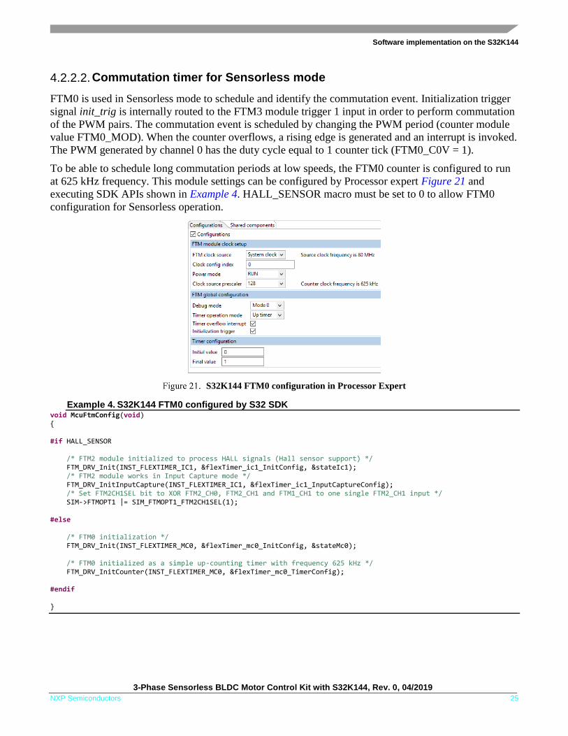
To be able to schedule long commutation periods at low speeds, the FTM0 counter is configured to run
at 625 kHz frequency. This module settings can be configured by Processor expert Figure 21 and
executing SDK APIs shown in Example 4. HALL_SENSOR macro must be set to 0 to allow FTM0
configuration for Sensorless operation.
S32K144 FTM0 configuration in Processor Expert
Example 4. S32K144 FTM0 configured by S32 SDK void McuFtmConfig(void) { #if HALL_SENSOR /* FTM2 module initialized to process HALL signals (Hall sensor support) */ FTM_DRV_Init(INST_FLEXTIMER_IC1, &flexTimer_ic1_InitConfig, &stateIc1); /* FTM2 module works in Input Capture mode */ FTM_DRV_InitInputCapture(INST_FLEXTIMER_IC1, &flexTimer_ic1_InputCaptureConfig); /* Set FTM2CH1SEL bit to XOR FTM2_CH0, FTM2_CH1 and FTM1_CH1 to one single FTM2_CH1 input */ SIM->FTMOPT1 |= SIM_FTMOPT1_FTM2CH1SEL(1); #else /* FTM0 initialization */ FTM_DRV_Init(INST_FLEXTIMER_MC0, &flexTimer_mc0_InitConfig, &stateMc0); /* FTM0 initialized as a simple up-counting timer with frequency 625 kHz */ FTM_DRV_InitCounter(INST_FLEXTIMER_MC0, &flexTimer_mc0_TimerConfig); #endif }
Software implementation on the S32K144
3-Phase Sensorless BLDC Motor Control Kit with S32K144, Rev. 0, 04/2019
26 NXP Semiconductors
4.2.2.3. Input capture mode and Hall sensor support
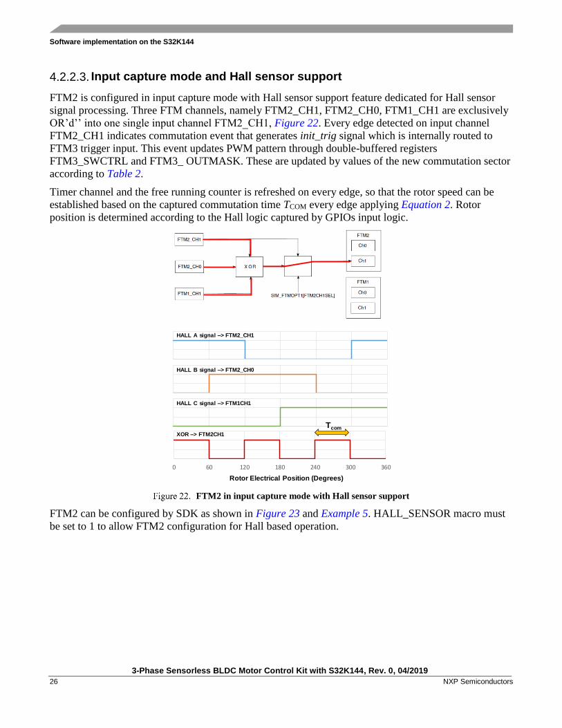
FTM2 is configured in input capture mode with Hall sensor support feature dedicated for Hall sensor
signal processing. Three FTM channels, namely FTM2_CH1, FTM2_CH0, FTM1_CH1 are exclusively
OR’d’’ into one single input channel FTM2_CH1, Figure 22. Every edge detected on input channel
FTM2_CH1 indicates commutation event that generates init_trig signal which is internally routed to
FTM3 trigger input. This event updates PWM pattern through double-buffered registers
FTM3_SWCTRL and FTM3_ OUTMASK. These are updated by values of the new commutation sector
according to Table 2.
Timer channel and the free running counter is refreshed on every edge, so that the rotor speed can be
established based on the captured commutation time TCOM every edge applying Equation 2. Rotor
position is determined according to the Hall logic captured by GPIOs input logic.
0 60 120 180 240 300 360
0 60 120 180 240 300 360
0 60 120 180 240 300 360
0 60 120 180 240 300 360
Rotor Electrical Position (Degrees)
HALL A signal –> FTM2_CH1
HALL B signal –> FTM2_CH0
HALL C signal –> FTM1CH1
XOR –> FTM2CH1
Tcom
FTM2 in input capture mode with Hall sensor support
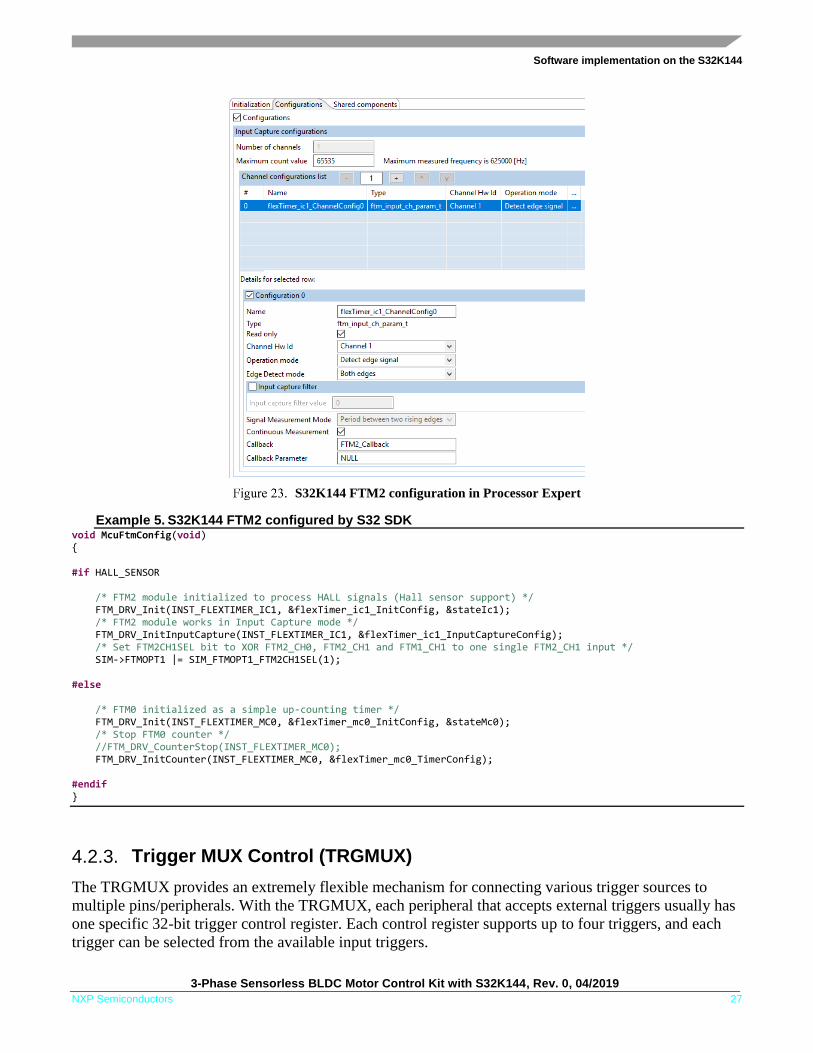
FTM2 can be configured by SDK as shown in Figure 23 and Example 5. HALL_SENSOR macro must
be set to 1 to allow FTM2 configuration for Hall based operation.
Software implementation on the S32K144
3-Phase Sensorless BLDC Motor Control Kit with S32K144, Rev. 0, 04/2019
NXP Semiconductors 27
S32K144 FTM2 configuration in Processor Expert
Example 5. S32K144 FTM2 configured by S32 SDK void McuFtmConfig(void) { #if HALL_SENSOR /* FTM2 module initialized to process HALL signals (Hall sensor support) */ FTM_DRV_Init(INST_FLEXTIMER_IC1, &flexTimer_ic1_InitConfig, &stateIc1); /* FTM2 module works in Input Capture mode */ FTM_DRV_InitInputCapture(INST_FLEXTIMER_IC1, &flexTimer_ic1_InputCaptureConfig); /* Set FTM2CH1SEL bit to XOR FTM2_CH0, FTM2_CH1 and FTM1_CH1 to one single FTM2_CH1 input */ SIM->FTMOPT1 |= SIM_FTMOPT1_FTM2CH1SEL(1); #else /* FTM0 initialized as a simple up-counting timer */ FTM_DRV_Init(INST_FLEXTIMER_MC0, &flexTimer_mc0_InitConfig, &stateMc0); /* Stop FTM0 counter */ //FTM_DRV_CounterStop(INST_FLEXTIMER_MC0); FTM_DRV_InitCounter(INST_FLEXTIMER_MC0, &flexTimer_mc0_TimerConfig); #endif }
4.2.3. Trigger MUX Control (TRGMUX)
The TRGMUX provides an extremely flexible mechanism for connecting various trigger sources to
multiple pins/peripherals. With the TRGMUX, each peripheral that accepts external triggers usually has
one specific 32-bit trigger control register. Each control register supports up to four triggers, and each
trigger can be selected from the available input triggers.
Software implementation on the S32K144
3-Phase Sensorless BLDC Motor Control Kit with S32K144, Rev. 0, 04/2019
28 NXP Semiconductors
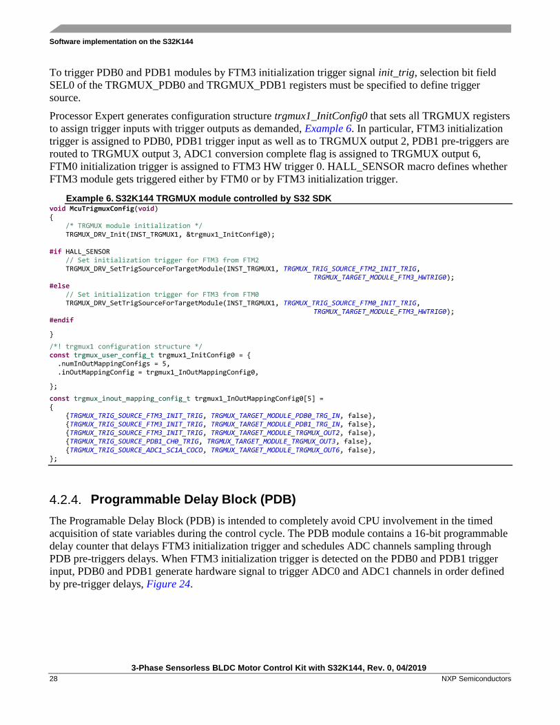
To trigger PDB0 and PDB1 modules by FTM3 initialization trigger signal init_trig, selection bit field
SEL0 of the TRGMUX_PDB0 and TRGMUX_PDB1 registers must be specified to define trigger
source.
Processor Expert generates configuration structure trgmux1_InitConfig0 that sets all TRGMUX registers
to assign trigger inputs with trigger outputs as demanded, Example 6. In particular, FTM3 initialization
trigger is assigned to PDB0, PDB1 trigger input as well as to TRGMUX output 2, PDB1 pre-triggers are
routed to TRGMUX output 3, ADC1 conversion complete flag is assigned to TRGMUX output 6,
FTM0 initialization trigger is assigned to FTM3 HW trigger 0. HALL_SENSOR macro defines whether
FTM3 module gets triggered either by FTM0 or by FTM3 initialization trigger.
Example 6. S32K144 TRGMUX module controlled by S32 SDK void McuTrigmuxConfig(void) { /* TRGMUX module initialization */ TRGMUX_DRV_Init(INST_TRGMUX1, &trgmux1_InitConfig0); #if HALL_SENSOR // Set initialization trigger for FTM3 from FTM2 TRGMUX_DRV_SetTrigSourceForTargetModule(INST_TRGMUX1, TRGMUX_TRIG_SOURCE_FTM2_INIT_TRIG, TRGMUX_TARGET_MODULE_FTM3_HWTRIG0); #else // Set initialization trigger for FTM3 from FTM0 TRGMUX_DRV_SetTrigSourceForTargetModule(INST_TRGMUX1, TRGMUX_TRIG_SOURCE_FTM0_INIT_TRIG, TRGMUX_TARGET_MODULE_FTM3_HWTRIG0); #endif
}
/*! trgmux1 configuration structure */ const trgmux_user_config_t trgmux1_InitConfig0 = { .numInOutMappingConfigs = 5, .inOutMappingConfig = trgmux1_InOutMappingConfig0,
};
const trgmux_inout_mapping_config_t trgmux1_InOutMappingConfig0[5] = { {TRGMUX_TRIG_SOURCE_FTM3_INIT_TRIG, TRGMUX_TARGET_MODULE_PDB0_TRG_IN, false}, {TRGMUX_TRIG_SOURCE_FTM3_INIT_TRIG, TRGMUX_TARGET_MODULE_PDB1_TRG_IN, false}, {TRGMUX_TRIG_SOURCE_FTM3_INIT_TRIG, TRGMUX_TARGET_MODULE_TRGMUX_OUT2, false}, {TRGMUX_TRIG_SOURCE_PDB1_CH0_TRIG, TRGMUX_TARGET_MODULE_TRGMUX_OUT3, false}, {TRGMUX_TRIG_SOURCE_ADC1_SC1A_COCO, TRGMUX_TARGET_MODULE_TRGMUX_OUT6, false}, };
4.2.4. Programmable Delay Block (PDB)
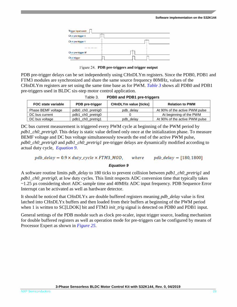
The Programable Delay Block (PDB) is intended to completely avoid CPU involvement in the timed
acquisition of state variables during the control cycle. The PDB module contains a 16-bit programmable
delay counter that delays FTM3 initialization trigger and schedules ADC channels sampling through
PDB pre-triggers delays. When FTM3 initialization trigger is detected on the PDB0 and PDB1 trigger
input, PDB0 and PDB1 generate hardware signal to trigger ADC0 and ADC1 channels in order defined
by pre-trigger delays, Figure 24.
Software implementation on the S32K144
3-Phase Sensorless BLDC Motor Control Kit with S32K144, Rev. 0, 04/2019
NXP Semiconductors 29
PDB pre-triggers and trigger output
PDB pre-trigger delays can be set independently using CHnDLYm registers. Since the PDB0, PDB1 and
FTM3 modules are synchronized and share the same source frequency 80MHz, values of the
CHnDLYm registers are set using the same time base as for PWM. Table 3 shows all PDB0 and PDB1
pre-triggers used in BLDC six-step motor control application.
Table 3. PDB0 and PDB1 pre-triggers
FOC state variable PDB pre-trigger CHnDLYm value [ticks] Relation to PWM
Phase BEMF voltage pdb0_ch0_pretrig0 pdb_delay At 90% of the active PWM pulse
DC bus current pdb1_ch0_pretrig0 0 At beginning of the PWM
DC bus voltage pdb1_ch0_pretrig1 pdb_delay At 90% of the active PWM pulse
DC bus current measurement is triggered every PWM cycle at beginning of the PWM period by
pdb1_ch0_pretrig0. This delay is static value defined only once at the initialization phase. To measure
BEMF voltage and DC bus voltage simultaneously towards the end of the active PWM pulse,
pdb0_ch0_pretrig0 and pdb1_ch0_pretrig1 pre-trigger delays are dynamically modified according to
actual duty cycle, Equation 9.
Equation 9
A software routine limits pdb_delay to 180 ticks to prevent collision between pdb1_ch0_pretrig1 and
pdb1_ch0_pretrig0, at low duty cycles. This limit respects ADC conversion time that typically takes
~1.25 µs considering short ADC sample time and 40MHz ADC input frequency. PDB Sequence Error
Interrupt can be activated as well as hardware detector.
It should be noticed that CHnDLYx are double buffered registers meaning pdb_delay value is first
latched into CHnDLYx buffers and then loaded from their buffers at beginning of the PWM period
when 1 is written to SC[LDOK] bit and FTM3 init_trig signal is detected on PDB0 and PDB1 input.
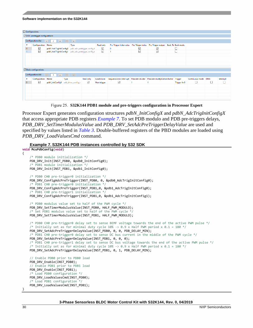
General settings of the PDB module such as clock pre-scaler, input trigger source, loading mechanism
for double buffered registers as well as operation mode for pre-triggers can be configured by means of
Processor Expert as shown in Figure 25.
Software implementation on the S32K144
3-Phase Sensorless BLDC Motor Control Kit with S32K144, Rev. 0, 04/2019
30 NXP Semiconductors
S32K144 PDB1 module and pre-triggers configuration in Processor Expert
Processor Expert generates configuration structures pdbN_InitConfigX and pdbN_AdcTrigInitConfigX
that access appropriate PDB registers Example 7. To set PDB modulo and PDB pre-triggers delays,
PDB_DRV_SetTimerModulusValue and PDB_DRV_SetAdcPreTriggerDelayValue are used and
specified by values listed in Table 3. Double-buffered registers of the PBD modules are loaded using
PDB_DRV_LoadValuesCmd command.
Example 7. S32K144 PDB instances controlled by S32 SDK void McuPdbConfig(void) { /* PDB0 module initialization */ PDB_DRV_Init(INST_PDB0, &pdb0_InitConfig0); /* PDB1 module initialization */ PDB_DRV_Init(INST_PDB1, &pdb1_InitConfig0); /* PDB0 CH0 pre-trigger0 initialization */ PDB_DRV_ConfigAdcPreTrigger(INST_PDB0, 0, &pdb0_AdcTrigInitConfig0); /* PDB1 CH0 pre-trigger0 initialization */ PDB_DRV_ConfigAdcPreTrigger(INST_PDB1,0, &pdb1_AdcTrigInitConfig0); /* PDB1 CH0 pre-trigger1 initialization */ PDB_DRV_ConfigAdcPreTrigger(INST_PDB1,0, &pdb1_AdcTrigInitConfig1); /* PDB0 modulus value set to half of the PWM cycle */ PDB_DRV_SetTimerModulusValue(INST_PDB0, HALF_PWM_MODULO); /* Set PDB1 modulus value set to half of the PWM cycle */ PDB_DRV_SetTimerModulusValue(INST_PDB1, HALF_PWM_MODULO); /* PDB0 CH0 pre-trigger0 delay set to sense BEMF voltage towards the end of the active PWM pulse */ /* Initially set as for minimal duty cycle 10% -> 0.9 x Half PWM period x 0.1 = 180 */ PDB_DRV_SetAdcPreTriggerDelayValue(INST_PDB0, 0, 0, PDB_DELAY_MIN); /* PDB1 CH0 pre-trigger0 delay set to sense DC bus current in the middle of the PWM cycle */ PDB_DRV_SetAdcPreTriggerDelayValue(INST_PDB1, 0, 0, 0); /* PDB1 CH0 pre-trigger1 delay set to sense DC bus voltage towards the end of the active PWM pulse */ /* Initially set as for minimal duty cycle 10% -> 0.9 x Half PWM period x 0.1 = 180 */ PDB_DRV_SetAdcPreTriggerDelayValue(INST_PDB1, 0, 1, PDB_DELAY_MIN); // Enable PDB0 prior to PDB0 load PDB_DRV_Enable(INST_PDB0); // Enable PDB1 prior to PDB1 load PDB_DRV_Enable(INST_PDB1); /* Load PDB0 configuration */ PDB_DRV_LoadValuesCmd(INST_PDB0); /* Load PDB1 configuration */ PDB_DRV_LoadValuesCmd(INST_PDB1); }
Software implementation on the S32K144
3-Phase Sensorless BLDC Motor Control Kit with S32K144, Rev. 0, 04/2019
NXP Semiconductors 31
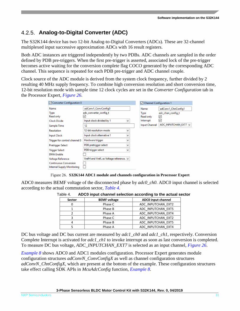
4.2.5. Analog-to-Digital Converter (ADC)
The S32K144 device has two 12-bit Analog-to-Digital Converters (ADCs). These are 32-channel
multiplexed input successive approximation ADCs with 16 result registers.
Both ADC instances are triggered independently by two PDBs. ADC channels are sampled in the order
defined by PDB pre-triggers. When the first pre-trigger is asserted, associated lock of the pre-trigger
becomes active waiting for the conversion complete flag COCO generated by the corresponding ADC
channel. This sequence is repeated for each PDB pre-trigger and ADC channel couple.
Clock source of the ADC module is derived from the system clock frequency, further divided by 2
resulting 40 MHz supply frequency. To combine high conversion resolution and short conversion time,
12-bit resolution mode with sample time 12 clock cycles are set in the Converter Configuration tab in
the Processor Expert, Figure 26.
S32K144 ADC1 module and channels configuration in Processor Expert
ADC0 measures BEMF voltage of the disconnected phase by adc0_ch0. ADC0 input channel is selected
according to the actual commutation sector, Table 4.
Table 4. ADC0 input channel selection according to the actual sector
Sector BEMF voltage ADC0 input channel
0 Phase C ADC_INPUTCHAN_EXT2
1 Phase B ADC_INPUTCHAN_EXT5
2 Phase A ADC_INPUTCHAN_EXT4
3 Phase C ADC_INPUTCHAN_EXT2
4 Phase B ADC_INPUTCHAN_EXT5
5 Phase A ADC_INPUTCHAN_EXT4
DC bus voltage and DC bus current are measured by adc1_ch0 and adc1_ch1, respectively. Conversion
Complete Interrupt is activated for adc1_ch1 to invoke interrupt as soon as last conversion is completed.
To measure DC bus voltage, ADC_INPUTCHAN_EXT7 is selected as an input channel, Figure 26.
Example 8 shows ADC0 and ADC1 modules configuration. Processor Expert generates module
configuration structures adConvN_ConvConfigX as well as channel configuration structures
adConvN_ChnConfigX, which are present at the bottom of the example. These configuration structures
take effect calling SDK APIs in McuAdcConfig function, Example 8.
Software implementation on the S32K144
3-Phase Sensorless BLDC Motor Control Kit with S32K144, Rev. 0, 04/2019
32 NXP Semiconductors
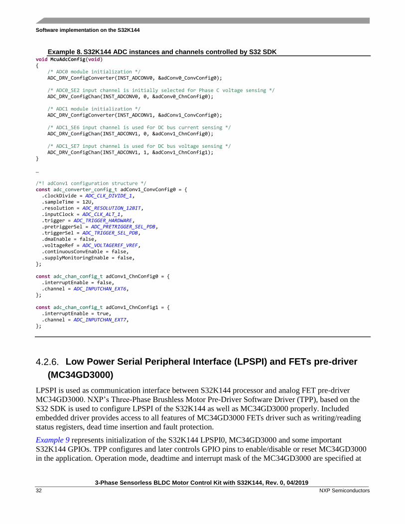
Example 8. S32K144 ADC instances and channels controlled by S32 SDK void McuAdcConfig(void) { /* ADC0 module initialization */ ADC_DRV_ConfigConverter(INST_ADCONV0, &adConv0_ConvConfig0); /* ADC0_SE2 input channel is initially selected for Phase C voltage sensing */ ADC_DRV_ConfigChan(INST_ADCONV0, 0, &adConv0_ChnConfig0); /* ADC1 module initialization */ ADC_DRV_ConfigConverter(INST_ADCONV1, &adConv1_ConvConfig0); /* ADC1_SE6 input channel is used for DC bus current sensing */ ADC_DRV_ConfigChan(INST_ADCONV1, 0, &adConv1_ChnConfig0); /* ADC1_SE7 input channel is used for DC bus voltage sensing */ ADC_DRV_ConfigChan(INST_ADCONV1, 1, &adConv1_ChnConfig1); } … /*! adConv1 configuration structure */ const adc_converter_config_t adConv1_ConvConfig0 = { .clockDivide = ADC_CLK_DIVIDE_1, .sampleTime = 12U, .resolution = ADC_RESOLUTION_12BIT, .inputClock = ADC_CLK_ALT_1, .trigger = ADC_TRIGGER_HARDWARE, .pretriggerSel = ADC_PRETRIGGER_SEL_PDB, .triggerSel = ADC_TRIGGER_SEL_PDB, .dmaEnable = false, .voltageRef = ADC_VOLTAGEREF_VREF, .continuousConvEnable = false, .supplyMonitoringEnable = false, }; const adc_chan_config_t adConv1_ChnConfig0 = { .interruptEnable = false, .channel = ADC_INPUTCHAN_EXT6, }; const adc_chan_config_t adConv1_ChnConfig1 = { .interruptEnable = true, .channel = ADC_INPUTCHAN_EXT7, };
4.2.6. Low Power Serial Peripheral Interface (LPSPI) and FETs pre-driver
(MC34GD3000)
LPSPI is used as communication interface between S32K144 processor and analog FET pre-driver
MC34GD3000. NXP’s Three-Phase Brushless Motor Pre-Driver Software Driver (TPP), based on the
S32 SDK is used to configure LPSPI of the S32K144 as well as MC34GD3000 properly. Included
embedded driver provides access to all features of MC34GD3000 FETs driver such as writing/reading
status registers, dead time insertion and fault protection.
Example 9 represents initialization of the S32K144 LPSPI0, MC34GD3000 and some important
S32K144 GPIOs. TPP configures and later controls GPIO pins to enable/disable or reset MC34GD3000
in the application. Operation mode, deadtime and interrupt mask of the MC34GD3000 are specified at
Software implementation on the S32K144
3-Phase Sensorless BLDC Motor Control Kit with S32K144, Rev. 0, 04/2019
NXP Semiconductors 33
next paragraphs. Parameters, such as LPSPI instance, chip select pin are defined at bottom of the
Example 9.
LPSPI0 communication frequency 2MHz is derived from the LPSPI0 input frequency 8MHz sourced
from the system oscillator clock (SOSC_CLK).
GPIOs, LPSPI0 and MC34GD3000 are configured and enabled by TPP_ConfigureGpio and
TPP_ConfigureSpi, TPP_Init functions, respectively.
Detailed description of the MC34GD3000 and its software driver (TPP) can be found at www.nxp.com.
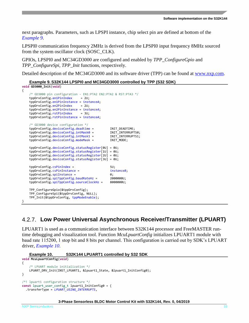
Example 9. S32K144 LPSPI0 and MC34GD3000 controlled by TPP (S32 SDK) void GD3000_Init(void) { /* GD3000 pin configuration - EN1:PTA2 EN2:PTA2 & RST:PTA3 */ tppDrvConfig.en1PinIndex = 2U; tppDrvConfig.en1PinInstance = instanceA; tppDrvConfig.en2PinIndex = 2U; tppDrvConfig.en2PinInstance = instanceA; tppDrvConfig.rstPinIndex = 3U; tppDrvConfig.rstPinInstance = instanceA; /* GD3000 device configuration */ tppDrvConfig.deviceConfig.deadtime = INIT_DEADTIME; tppDrvConfig.deviceConfig.intMask0 = INIT_INTERRUPTS0; tppDrvConfig.deviceConfig.intMask1 = INIT_INTERRUPTS1; tppDrvConfig.deviceConfig.modeMask = INIT_MODE; tppDrvConfig.deviceConfig.statusRegister[0U] = 0U; tppDrvConfig.deviceConfig.statusRegister[1U] = 0U; tppDrvConfig.deviceConfig.statusRegister[2U] = 0U; tppDrvConfig.deviceConfig.statusRegister[3U] = 0U; tppDrvConfig.csPinIndex = 5U; tppDrvConfig.csPinInstance = instanceB; tppDrvConfig.spiInstance = 0; tppDrvConfig.spiTppConfig.baudRateHz = 2000000U; tppDrvConfig.spiTppConfig.sourceClockHz = 8000000U; TPP_ConfigureGpio(&tppDrvConfig); TPP_ConfigureSpi(&tppDrvConfig, NULL); TPP_Init(&tppDrvConfig, tppModeEnable); }
4.2.7. Low Power Universal Asynchronous Receiver/Transmitter (LPUART)
LPUART1 is used as a communication interface between S32K144 processor and FreeMASTER run-
time debugging and visualization tool. Function McuLpuartConfig initializes LPUART1 module with
baud rate 115200, 1 stop bit and 8 bits per channel. This configuration is carried out by SDK’s LPUART
driver, Example 10.
Example 10. S32K144 LPUART1 controlled by S32 SDK void McuLpuartConfig(void) { /* LPUART module initialization */ LPUART_DRV_Init(INST_LPUART1, &lpuart1_State, &lpuart1_InitConfig0); } /*! lpuart1 configuration structure */ const lpuart_user_config_t lpuart1_InitConfig0 = { .transferType = LPUART_USING_INTERRUPTS,
Software implementation on the S32K144
3-Phase Sensorless BLDC Motor Control Kit with S32K144, Rev. 0, 04/2019
34 NXP Semiconductors
.baudRate = 115200U, .parityMode = LPUART_PARITY_DISABLED, .stopBitCount = LPUART_ONE_STOP_BIT, .bitCountPerChar = LPUART_8_BITS_PER_CHAR, .rxDMAChannel = 0U, .txDMAChannel = 0U, };
Configuration structure lpuart1_InitConfig0 can be modified manually or configured by means of
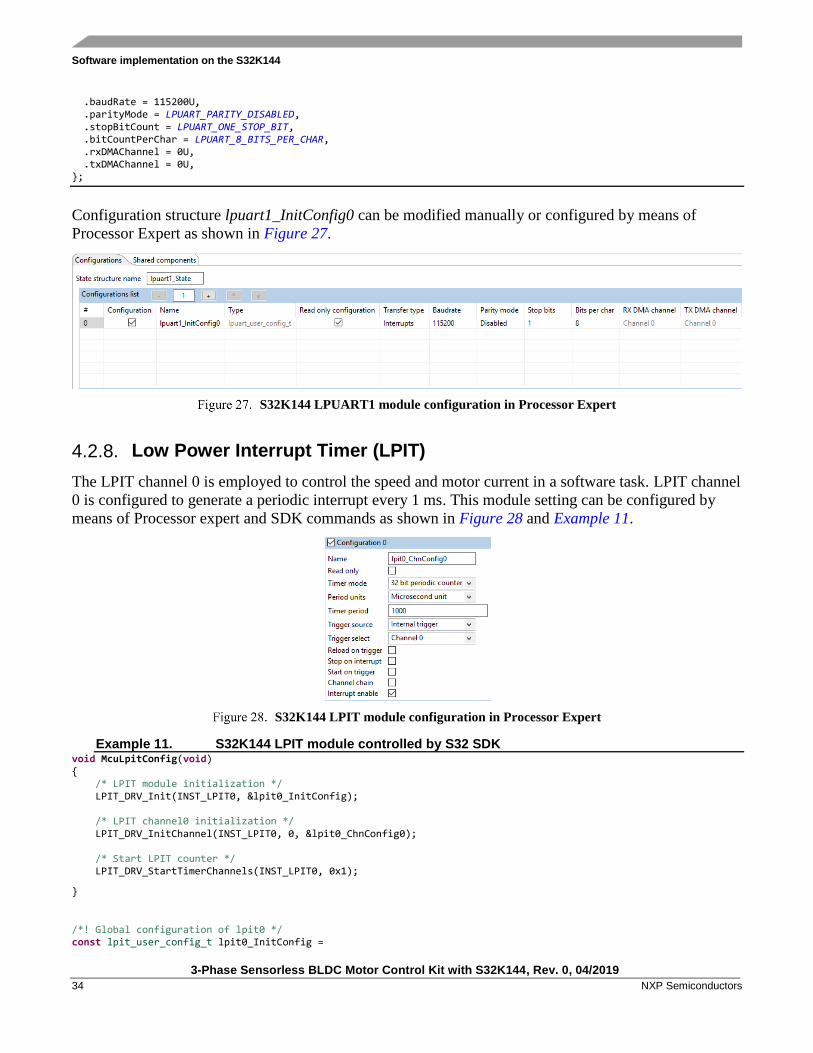
Processor Expert as shown in Figure 27.
S32K144 LPUART1 module configuration in Processor Expert
4.2.8. Low Power Interrupt Timer (LPIT)
The LPIT channel 0 is employed to control the speed and motor current in a software task. LPIT channel
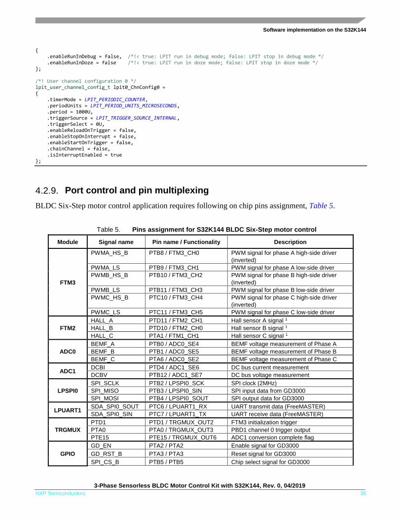
0 is configured to generate a periodic interrupt every 1 ms. This module setting can be configured by
means of Processor expert and SDK commands as shown in Figure 28 and Example 11.
S32K144 LPIT module configuration in Processor Expert
Example 11. S32K144 LPIT module controlled by S32 SDK void McuLpitConfig(void) { /* LPIT module initialization */ LPIT_DRV_Init(INST_LPIT0, &lpit0_InitConfig); /* LPIT channel0 initialization */ LPIT_DRV_InitChannel(INST_LPIT0, 0, &lpit0_ChnConfig0); /* Start LPIT counter */ LPIT_DRV_StartTimerChannels(INST_LPIT0, 0x1);
}
/*! Global configuration of lpit0 */ const lpit_user_config_t lpit0_InitConfig =
Software implementation on the S32K144
3-Phase Sensorless BLDC Motor Control Kit with S32K144, Rev. 0, 04/2019
NXP Semiconductors 35
{ .enableRunInDebug = false, /*!< true: LPIT run in debug mode; false: LPIT stop in debug mode */ .enableRunInDoze = false /*!< true: LPIT run in doze mode; false: LPIT stop in doze mode */ }; /*! User channel configuration 0 */ lpit_user_channel_config_t lpit0_ChnConfig0 = { .timerMode = LPIT_PERIODIC_COUNTER, .periodUnits = LPIT_PERIOD_UNITS_MICROSECONDS, .period = 1000U, .triggerSource = LPIT_TRIGGER_SOURCE_INTERNAL, .triggerSelect = 0U, .enableReloadOnTrigger = false, .enableStopOnInterrupt = false, .enableStartOnTrigger = false, .chainChannel = false, .isInterruptEnabled = true };
4.2.9. Port control and pin multiplexing
BLDC Six-Step motor control application requires following on chip pins assignment, Table 5.
Table 5. Pins assignment for S32K144 BLDC Six-Step motor control
Module Signal name Pin name / Functionality Description
FTM3
PWMA_HS_B PTB8 / FTM3_CH0 PWM signal for phase A high-side driver
(inverted)
PWMA_LS PTB9 / FTM3_CH1 PWM signal for phase A low-side driver
PWMB_HS_B PTB10 / FTM3_CH2 PWM signal for phase B high-side driver
(inverted)
PWMB_LS PTB11 / FTM3_CH3 PWM signal for phase B low-side driver
PWMC_HS_B PTC10 / FTM3_CH4 PWM signal for phase C high-side driver
(inverted)
PWMC_LS PTC11 / FTM3_CH5 PWM signal for phase C low-side driver
FTM2
HALL_A PTD11 / FTM2_CH1 Hall sensor A signal 1
HALL_B PTD10 / FTM2_CH0 Hall sensor B signal 1
HALL_C PTA1 / FTM1_CH1 Hall sensor C signal 1
ADC0
BEMF_A PTB0 / ADC0_SE4 BEMF voltage measurement of Phase A
BEMF_B PTB1 / ADC0_SE5 BEMF voltage measurement of Phase B
BEMF_C PTA6 / ADC0_SE2 BEMF voltage measurement of Phase C
ADC1 DCBI PTD4 / ADC1_SE6 DC bus current measurement
DCBV PTB12 / ADC1_SE7 DC bus voltage measurement
LPSPI0
SPI_SCLK PTB2 / LPSPI0_SCK SPI clock (2MHz)
SPI_MISO PTB3 / LPSPI0_SIN SPI input data from GD3000
SPI_MOSI PTB4 / LPSPI0_SOUT SPI output data for GD3000
LPUART1 SDA_SPI0_SOUT PTC6 / LPUART1_RX UART transmit data (FreeMASTER)
SDA_SPI0_SIN PTC7 / LPUART1_TX UART receive data (FreeMASTER)
TRGMUX
PTD1 PTD1 / TRGMUX_OUT2 FTM3 initialization trigger
PTA0 PTA0 / TRGMUX_OUT3 PBD1 channel 0 trigger output
PTE15 PTE15 / TRGMUX_OUT6 ADC1 conversion complete flag
GPIO
GD_EN PTA2 / PTA2 Enable signal for GD3000
GD_RST_B PTA3 / PTA3 Reset signal for GD3000
SPI_CS_B PTB5 / PTB5 Chip select signal for GD3000
Software implementation on the S32K144
3-Phase Sensorless BLDC Motor Control Kit with S32K144, Rev. 0, 04/2019
36 NXP Semiconductors
BTN0 PTC12 / PTC12 Application control via board button
BTN1 PTC13 / PTC13 Application control via board button
RGB_BLUE PTD0 / PTD0 RGB_BLUE indicating run state
PTD2 PTD2 / PTD2 GPIO toggling to measure execution time
BRAKE_PWM PTD14 / PTD14 Connecting / disconnecting braking resistor
RGB_RED PTD15 / PTD15 RGB_RED indicating fault state
RGB_GREEN PTD16 / PTD16 RGB_GREEN indicating ready/calib state
GD_INT PTE10 / PTE10 Interrupt signal indicating GD3000 fault 1 FTM module with Hall support feature OR’ds FTM2_CH0, FTM2_CH1, FTM1_CH0 input pins into one single
FTM channel FTM2_CH1 that works in input capture mode. See section Input capture mode and Hall sensor
support for more details.
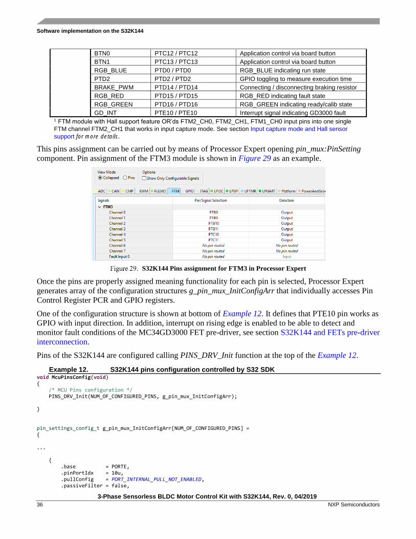
This pins assignment can be carried out by means of Processor Expert opening pin_mux:PinSetting
component. Pin assignment of the FTM3 module is shown in Figure 29 as an example.
S32K144 Pins assignment for FTM3 in Processor Expert
Once the pins are properly assigned meaning functionality for each pin is selected, Processor Expert
generates array of the configuration structures g_pin_mux_InitConfigArr that individually accesses Pin
Control Register PCR and GPIO registers.
One of the configuration structure is shown at bottom of Example 12. It defines that PTE10 pin works as
GPIO with input direction. In addition, interrupt on rising edge is enabled to be able to detect and
monitor fault conditions of the MC34GD3000 FET pre-driver, see section S32K144 and FETs pre-driver
interconnection.
Pins of the S32K144 are configured calling PINS_DRV_Init function at the top of the Example 12.
Example 12. S32K144 pins configuration controlled by S32 SDK void McuPinsConfig(void) { /* MCU Pins configuration */ PINS_DRV_Init(NUM_OF_CONFIGURED_PINS, g_pin_mux_InitConfigArr); } pin_settings_config_t g_pin_mux_InitConfigArr[NUM_OF_CONFIGURED_PINS] = { ... { .base = PORTE, .pinPortIdx = 10u, .pullConfig = PORT_INTERNAL_PULL_NOT_ENABLED, .passiveFilter = false,
Software implementation on the S32K144
3-Phase Sensorless BLDC Motor Control Kit with S32K144, Rev. 0, 04/2019
NXP Semiconductors 37
.driveSelect = PORT_LOW_DRIVE_STRENGTH, .mux = PORT_MUX_AS_GPIO, .pinLock = false, .intConfig = PORT_INT_RISING_EDGE, .clearIntFlag = false, .gpioBase = PTE, .direction = GPIO_INPUT_DIRECTION, .digitalFilter = false, }, ... }
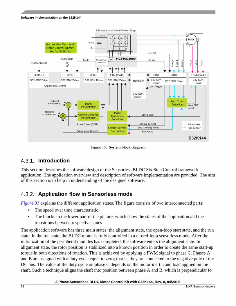
4.3. Software architecture
Figure 30 presents the conceptual system block diagram of the BLDC Six-step control technique
working either in sensorless or Hall sensor-based mode. This section is focused on the software design
of the Sensorless algorithm based on the zero-crossing detection technique.
The application is optimized for S32K144 motor control peripherals to achieve the least possible core
involvement in state variable acquisition and output action application. The motor control peripherals
(FTM0/FTM2, FTM3, PDB0, PDB1, ADC0, ADC1) are internally linked together to work
independently from the core, and to achieve deterministic sampling of analog quantities and precise
commutation of the stator field. The software part of the application consists of different blocks which
are described below. The entire application behavior is controlled from a PC through the FreeMASTER
run-time debugging tool.
The system block diagram is shown in Figure 30. The motor control algorithm blocks utilize the
Automotive Math and Motor control Library for ARM Cortex-M4(see section References).
The inputs of the control loop are the measured voltages and current on the power stage, in particular
the phase voltages, the DC bus current, and DC bus voltage. The DC bus current is amplified by the
current sense amplifier, which is part of the MC34GD3000 FET pre-driver, and then routed together
with the DC bus voltage and phase voltages to the ADC for measurement acquisition. From a control perspective, the block diagram can be divided into two logical parts:
• Commutation control, where the phase voltages and DC bus voltage are used to calculate the
actual position of the shaft. According to the identified position, the next commutation event can
be prepared. • Speed/torque control, where the required shaft velocity is compared to the actual measured
speed and regulated by the PI controller. The output of the speed PI controller is the duty cycle.
The duty cycle is limited by the current PI controller and assigned to the PWM.
Software implementation on the S32K144
3-Phase Sensorless BLDC Motor Control Kit with S32K144, Rev. 0, 04/2019
38 NXP Semiconductors
System block diagram
4.3.1. Introduction
This section describes the software design of the Sensorless BLDC Six Step Control framework
application. The application overview and description of software implementation are provided. The aim
of this section is to help in understanding of the designed software.
4.3.2. Application flow in Sensorless mode
Figure 31 explains the different application states. The figure consists of two interconnected parts:
• The speed over time characteristic • The blocks in the lower part of the picture, which show the states of the application and the
transitions between respective states The application software has three main states: the alignment state, the open-loop start state, and the run
state. In the run state, the BLDC motor is fully controlled in a closed-loop sensorless mode. After the
initialization of the peripheral modules has completed, the software enters the alignment state. In
alignment state, the rotor position is stabilized into a known position in order to create the same start-up
torque in both directions of rotation. This is achieved by applying a PWM signal to phase C. Phases A
and B are assigned with a duty cycle equal to zero; that is, they are connected to the negative pole of the
DC bus. The value of the duty cycle on phase C depends on the motor inertia and load applied on the
shaft. Such a technique aligns the shaft into position between phase A and B, which is perpendicular to
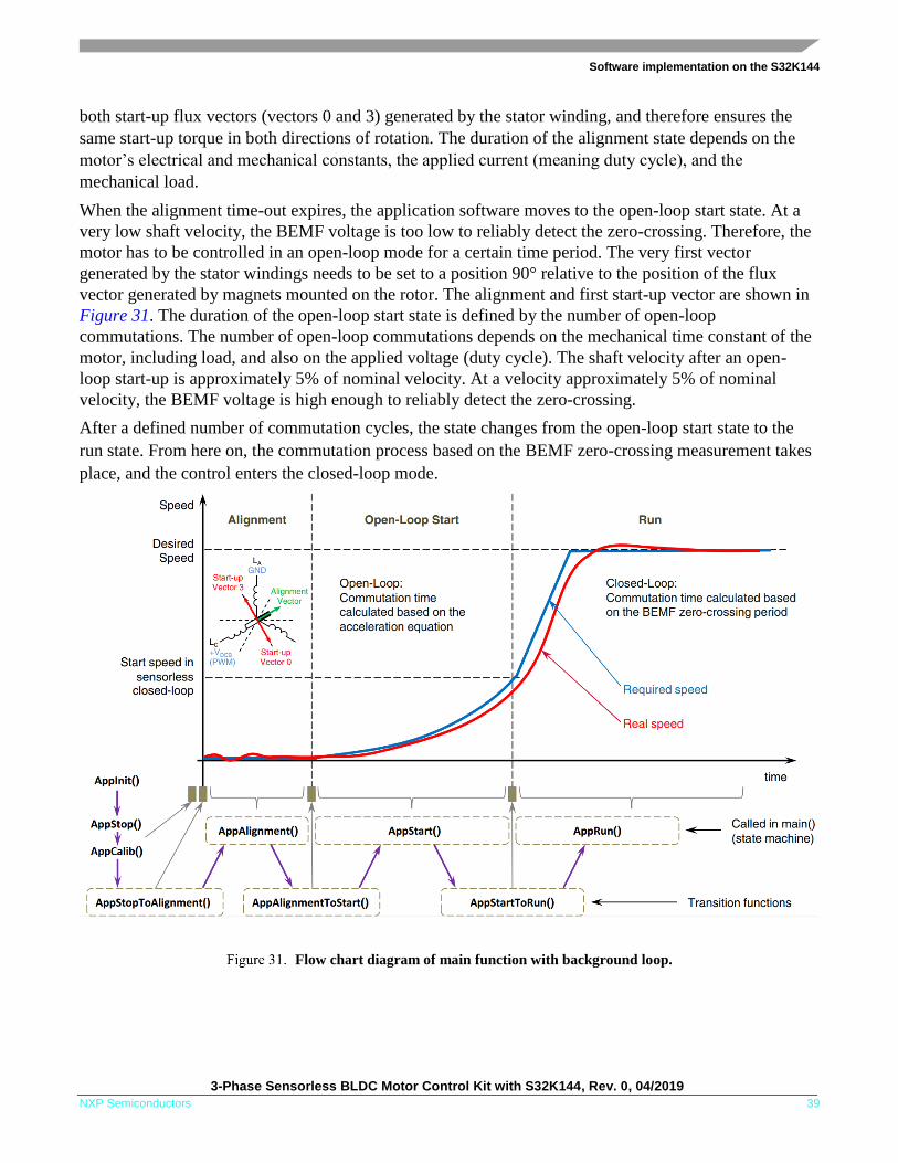
Software implementation on the S32K144
3-Phase Sensorless BLDC Motor Control Kit with S32K144, Rev. 0, 04/2019
NXP Semiconductors 39
both start-up flux vectors (vectors 0 and 3) generated by the stator winding, and therefore ensures the
same start-up torque in both directions of rotation. The duration of the alignment state depends on the
motor’s electrical and mechanical constants, the applied current (meaning duty cycle), and the
mechanical load. When the alignment time-out expires, the application software moves to the open-loop start state. At a
very low shaft velocity, the BEMF voltage is too low to reliably detect the zero-crossing. Therefore, the
motor has to be controlled in an open-loop mode for a certain time period. The very first vector
generated by the stator windings needs to be set to a position 90° relative to the position of the flux
vector generated by magnets mounted on the rotor. The alignment and first start-up vector are shown in
Figure 31. The duration of the open-loop start state is defined by the number of open-loop
commutations. The number of open-loop commutations depends on the mechanical time constant of the
motor, including load, and also on the applied voltage (duty cycle). The shaft velocity after an open-
loop start-up is approximately 5% of nominal velocity. At a velocity approximately 5% of nominal
velocity, the BEMF voltage is high enough to reliably detect the zero-crossing. After a defined number of commutation cycles, the state changes from the open-loop start state to the
run state. From here on, the commutation process based on the BEMF zero-crossing measurement takes
place, and the control enters the closed-loop mode.
Flow chart diagram of main function with background loop.
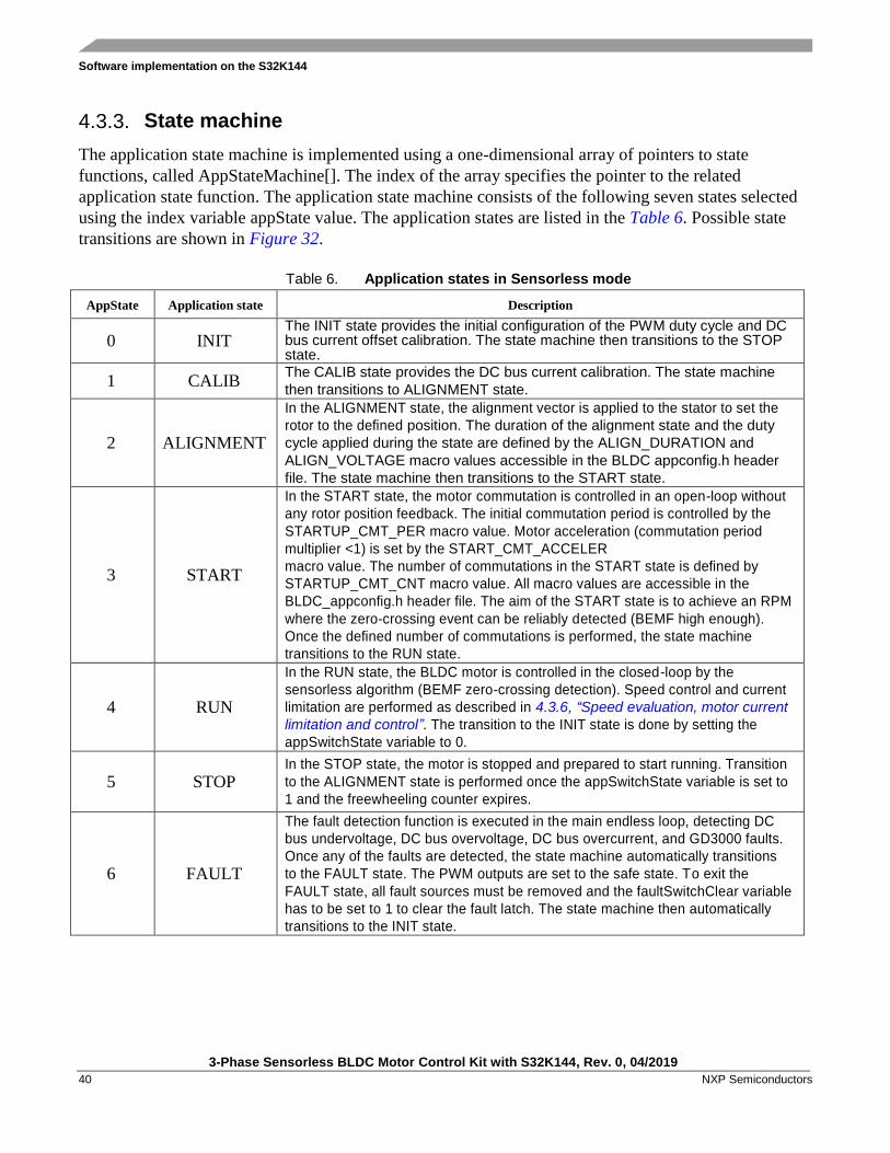
Software implementation on the S32K144
3-Phase Sensorless BLDC Motor Control Kit with S32K144, Rev. 0, 04/2019
40 NXP Semiconductors
4.3.3. State machine
The application state machine is implemented using a one-dimensional array of pointers to state
functions, called AppStateMachine[]. The index of the array specifies the pointer to the related
application state function. The application state machine consists of the following seven states selected
using the index variable appState value. The application states are listed in the Table 6. Possible state
transitions are shown in Figure 32.
Table 6. Application states in Sensorless mode
AppState Application state Description
0 INIT The INIT state provides the initial configuration of the PWM duty cycle and DC bus current offset calibration. The state machine then transitions to the STOP state.
1 CALIB The CALIB state provides the DC bus current calibration. The state machine
then transitions to ALIGNMENT state.
2 ALIGNMENT
In the ALIGNMENT state, the alignment vector is applied to the stator to set the
rotor to the defined position. The duration of the alignment state and the duty
cycle applied during the state are defined by the ALIGN_DURATION and
ALIGN_VOLTAGE macro values accessible in the BLDC appconfig.h header
file. The state machine then transitions to the START state.
3 START
In the START state, the motor commutation is controlled in an open-loop without
any rotor position feedback. The initial commutation period is controlled by the
STARTUP_CMT_PER macro value. Motor acceleration (commutation period
multiplier <1) is set by the START_CMT_ACCELER
macro value. The number of commutations in the START state is defined by
STARTUP_CMT_CNT macro value. All macro values are accessible in the
BLDC_appconfig.h header file. The aim of the START state is to achieve an RPM
where the zero-crossing event can be reliably detected (BEMF high enough).
Once the defined number of commutations is performed, the state machine
transitions to the RUN state.
4 RUN
In the RUN state, the BLDC motor is controlled in the closed-loop by the
sensorless algorithm (BEMF zero-crossing detection). Speed control and current
limitation are performed as described in 4.3.6, “Speed evaluation, motor current
limitation and control”. The transition to the INIT state is done by setting the
appSwitchState variable to 0.
5 STOP In the STOP state, the motor is stopped and prepared to start running. Transition
to the ALIGNMENT state is performed once the appSwitchState variable is set to
1 and the freewheeling counter expires.
6 FAULT
The fault detection function is executed in the main endless loop, detecting DC
bus undervoltage, DC bus overvoltage, DC bus overcurrent, and GD3000 faults.
Once any of the faults are detected, the state machine automatically transitions
to the FAULT state. The PWM outputs are set to the safe state. To exit the
FAULT state, all fault sources must be removed and the faultSwitchClear variable
has to be set to 1 to clear the fault latch. The state machine then automatically
transitions to the INIT state.
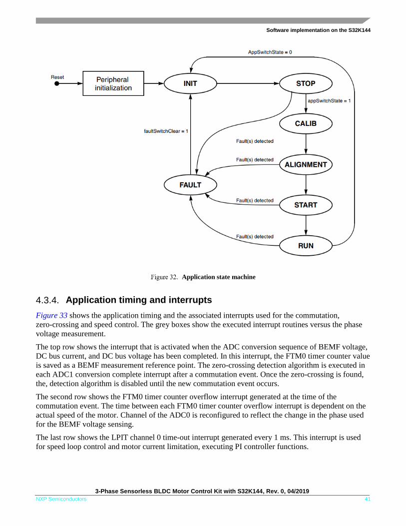
Software implementation on the S32K144
3-Phase Sensorless BLDC Motor Control Kit with S32K144, Rev. 0, 04/2019
NXP Semiconductors 41
Application state machine
4.3.4. Application timing and interrupts
Figure 33 shows the application timing and the associated interrupts used for the commutation,
zero-crossing and speed control. The grey boxes show the executed interrupt routines versus the phase
voltage measurement.
The top row shows the interrupt that is activated when the ADC conversion sequence of BEMF voltage,
DC bus current, and DC bus voltage has been completed. In this interrupt, the FTM0 timer counter value
is saved as a BEMF measurement reference point. The zero-crossing detection algorithm is executed in
each ADC1 conversion complete interrupt after a commutation event. Once the zero-crossing is found,
the, detection algorithm is disabled until the new commutation event occurs.
The second row shows the FTM0 timer counter overflow interrupt generated at the time of the
commutation event. The time between each FTM0 timer counter overflow interrupt is dependent on the
actual speed of the motor. Channel of the ADC0 is reconfigured to reflect the change in the phase used
for the BEMF voltage sensing.
The last row shows the LPIT channel 0 time-out interrupt generated every 1 ms. This interrupt is used
for speed loop control and motor current limitation, executing PI controller functions.
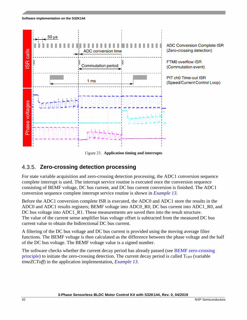
Software implementation on the S32K144
3-Phase Sensorless BLDC Motor Control Kit with S32K144, Rev. 0, 04/2019
42 NXP Semiconductors
Application timing and interrupts
4.3.5. Zero-crossing detection processing
For state variable acquisition and zero-crossing detection processing, the ADC1 conversion sequence
complete interrupt is used. The interrupt service routine is executed once the conversion sequence
consisting of BEMF voltage, DC bus current, and DC bus current conversion is finished. The ADC1
conversion sequence complete interrupt service routine is shown in Example 13.
Before the ADC1 conversion complete ISR is executed, the ADC0 and ADC1 store the results in the
ADC0 and ADC1 results registers; BEMF voltage into ADC0_R0, DC bus current into ADC1_R0, and
DC bus voltage into ADC1_R1. These measurements are saved then into the result structure.
The value of the current sense amplifier bias voltage offset is subtracted from the measured DC bus
current value to obtain the bidirectional DC bus current.
A filtering of the DC bus voltage and DC bus current is provided using the moving average filter
functions. The BEMF voltage is then calculated as the difference between the phase voltage and the half
of the DC bus voltage. The BEMF voltage value is a signed number.
The software checks whether the current decay period has already passed (see BEMF zero-crossing
principle) to initiate the zero-crossing detection. The current decay period is called TOFF (variable
timeZCToff) in the application implementation, Example 13.
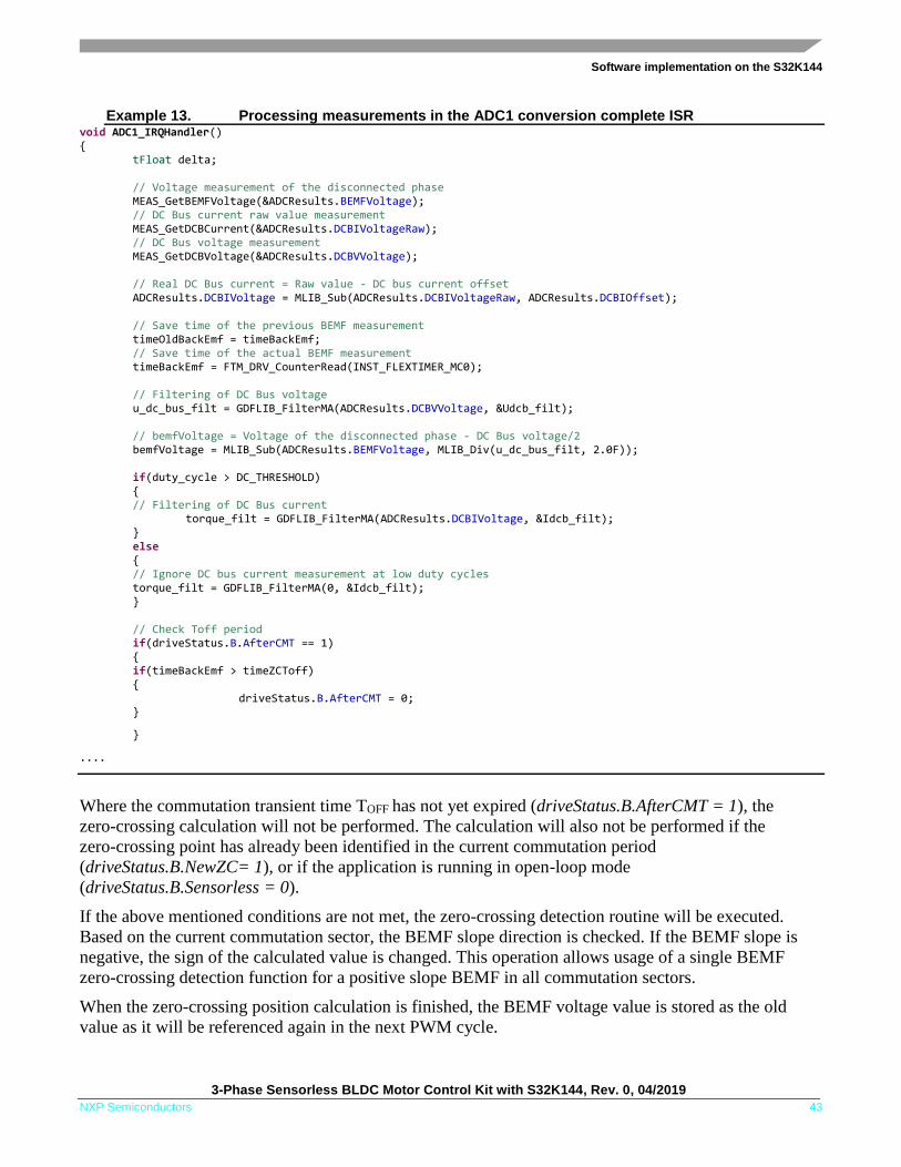
Software implementation on the S32K144
3-Phase Sensorless BLDC Motor Control Kit with S32K144, Rev. 0, 04/2019
NXP Semiconductors 43
Example 13. Processing measurements in the ADC1 conversion complete ISR void ADC1_IRQHandler() { tFloat delta; // Voltage measurement of the disconnected phase MEAS_GetBEMFVoltage(&ADCResults.BEMFVoltage); // DC Bus current raw value measurement MEAS_GetDCBCurrent(&ADCResults.DCBIVoltageRaw); // DC Bus voltage measurement MEAS_GetDCBVoltage(&ADCResults.DCBVVoltage); // Real DC Bus current = Raw value - DC bus current offset ADCResults.DCBIVoltage = MLIB_Sub(ADCResults.DCBIVoltageRaw, ADCResults.DCBIOffset); // Save time of the previous BEMF measurement timeOldBackEmf = timeBackEmf; // Save time of the actual BEMF measurement timeBackEmf = FTM_DRV_CounterRead(INST_FLEXTIMER_MC0); // Filtering of DC Bus voltage
u_dc_bus_filt = GDFLIB_FilterMA(ADCResults.DCBVVoltage, &Udcb_filt); // bemfVoltage = Voltage of the disconnected phase - DC Bus voltage/2 bemfVoltage = MLIB_Sub(ADCResults.BEMFVoltage, MLIB_Div(u_dc_bus_filt, 2.0F)); if(duty_cycle > DC_THRESHOLD) { // Filtering of DC Bus current
torque_filt = GDFLIB_FilterMA(ADCResults.DCBIVoltage, &Idcb_filt); } else { // Ignore DC bus current measurement at low duty cycles torque_filt = GDFLIB_FilterMA(0, &Idcb_filt); } // Check Toff period if(driveStatus.B.AfterCMT == 1) { if(timeBackEmf > timeZCToff) { driveStatus.B.AfterCMT = 0; }
}
....
Where the commutation transient time TOFF has not yet expired (driveStatus.B.AfterCMT = 1), the
zero-crossing calculation will not be performed. The calculation will also not be performed if the
zero-crossing point has already been identified in the current commutation period
(driveStatus.B.NewZC= 1), or if the application is running in open-loop mode
(driveStatus.B.Sensorless = 0).
If the above mentioned conditions are not met, the zero-crossing detection routine will be executed.
Based on the current commutation sector, the BEMF slope direction is checked. If the BEMF slope is
negative, the sign of the calculated value is changed. This operation allows usage of a single BEMF
zero-crossing detection function for a positive slope BEMF in all commutation sectors.
When the zero-crossing position calculation is finished, the BEMF voltage value is stored as the old
value as it will be referenced again in the next PWM cycle.
Software implementation on the S32K144
3-Phase Sensorless BLDC Motor Control Kit with S32K144, Rev. 0, 04/2019
44 NXP Semiconductors
Code listing in Example 15 describes the zero-crossing detection routine that was called in the interrupt
shown before.
Example 14. S32K144 BEMF Zero-crossing detection control
....
if((driveStatus.B.AfterCMT == 0) && (driveStatus.B.NewZC == 0) && (driveStatus.B.Sensorless == 1)) { /* If the BEMF voltage is falling, invert BEMF voltage value */ if((ActualCmtSector & 0x01) == 0) { bemfVoltage = -bemfVoltage; } /* Rising BEMF zero-crossing detection */ .... Save actual BEMF voltage (for ADC samples interpolation) bemfVoltageOld = bemfVoltage; driveStatus.B.AdcSaved = 1; } // Calibration timer for DC bus current offset measurement if(driveStatus.B.Calib) { calibTimer--; } // Application variables record FMSTR_Recorder();
}
In the case of a negative BEMF voltage (VBEMF < VDCB / 2), the zero-crossing point has not been
passed and the zero-crossing is not detectable. The software exits the zero-crossing detecting routine and
leaves the zero-crossing status bit unchanged (driveStatus.B.NewZC = 0). In the case of a zero or a
positive BEMF voltage (VBEMF ≥ VDCB / 2), the zero-crossing point was reached or passed and
Equation 7 is calculated, meaning that the BEMF voltage is divided by the delta of the two measured
points and multiplied by the measured PWM period (BEMF measurement period). After this calculation,
the old zero-crossing time and the new one are saved into the appropriate variables. The zero-crossing
period is then calculated based on the calculated time of zero-crossing and the time of the zero-crossing
in the previous commutation cycle. The zero-crossing period is also filtered to improve reliability
At the end of the routine, the new commutation time is calculated. Here, some motor characteristics
have to be taken into account. Instead of just adding half of a zero-crossing period to the actual zero-
crossing time, a so-called advance angle factor is taken into account, which actually activates the
commutation a bit earlier than calculated. This is usually a constant and depends on the motor
characteristics.
Finally, the zero-crossing status bit is set (driveStatus.B.NewZC = 1), so the zero-crossing detection
does not take place anymore in the current commutation cycle.
Software implementation on the S32K144
3-Phase Sensorless BLDC Motor Control Kit with S32K144, Rev. 0, 04/2019
NXP Semiconductors 45
Example 15. S32K144 BEMF Zero-crossing detection algorithm /* Rising BEMF zero-crossing detection */ if(bemfVoltage >= 0) { /* Rising interpolation */ delta = bemfVoltage - bemfVoltageOld; // Save delta of two measured points if((driveStatus.B.AdcSaved == 1) && (delta > bemfVoltage)) {
// Zero-crossing time calculation timeBackEmf -= MLIB_Mul(MLIB_Div(bemfVoltage, delta), MLIB_Sub(timeBackEmf, timeOldBackEmf));
} else {
// Zero-crossing time calculation timeBackEmf -= (MLIB_Div(MLIB_Sub(timeBackEmf, timeOldBackEmf), 2));
} // Save previous and actual zero-crossing time lastTimeZC = timeZC; timeZC = (uint16_t)timeBackEmf; // periodZC = (timeZC - lasTimeZC) + ftm_mod_old(no timer reset) periodZC[ActualCmtSector] = (ftm_mod_old - lastTimeZC) + timeZC; // Average of the previous and current ZC period actualPeriodZC = (actualPeriodZC + periodZC[ActualCmtSector]) >> 1; // advancedAngle(0.3815) = 0.5 * Advanced Angle(0.763) NextCmtPeriod = MLIB_Mul_F16(actualPeriodZC, advanceAngle); // Update commutation period -> FTM0_MOD = timeZC + nextCmtPeriod FTM_DRV_CounterStop(INST_FLEXTIMER_MC0); FTM_DRV_SetModuloCounterValue(INST_FLEXTIMER_MC0,timeZC+NextCmtPeriod, false); FTM_DRV_CounterStart(INST_FLEXTIMER_MC0); driveStatus.B.NewZC = 1;
}
4.3.6. Speed evaluation, motor current limitation and control
The speed controller in Example 16 is executed in a timer interrupt every 1 ms. First of all, the actual
speed is calculated from all of the last six zero-crossing periods, and this is stored as the actual speed.
The required speed is fed into the ramp function controlling the motor speed slope. The difference
between the speed ramp function output and actual speed defines the speed error.
In the closed-loop mode, the actual speed error is fed into the PI controller function. Inputs to the PI
controller function include the speed error and the PI controller’s parameters such as the proportional
and integral gain constants. The output of the PI controller is the duty cycle, which is scaled to the PWM
resolution.
At the end of the speed control function, the duty cycle is loaded into the FTM3 PWM module.
Software implementation on the S32K144
3-Phase Sensorless BLDC Motor Control Kit with S32K144, Rev. 0, 04/2019
46 NXP Semiconductors
Example 16. S32K144 Speed evaluation software flow void LPIT0_Ch0_IRQHandler() { uint8_t i; PTD->PSOR |= 1<<2; if(driveStatus.B.CloseLoop == 1) { torqueErr = MLIB_Sub(I_DCB_LIMIT, torque_filt); currentPIOut = GFLIB_ControllerPIpAW(torqueErr, ¤tPIPrms); /* Speed control */ period6ZC = periodZC[0]; for(i=1;i<6;i++) { period6ZC += periodZC[i]; } // Calculate actual rotor speed based on the BEMF zero cross period
actualSpeed = MLIB_Mul(MLIB_ConvertPU_FLTF32(MLIB_Div_F32(SPEED_SCALE_CONST, period6ZC)), N_MAX);
// Upper speed limit due to the limited DC bus voltage 12V if(requiredSpeed >= N_NOM) requiredSpeed = N_NOM; // Lower speed limit keeping reliable sensorless operation if(requiredSpeed < mcat_NMin) requiredSpeed = mcat_NMin; requiredSpeedRamp = GFLIB_Ramp(requiredSpeed, &speedRampPrms); speedErr = MLIB_Sub(requiredSpeedRamp, actualSpeed); speedPIOut = GFLIB_ControllerPIpAW(speedErr, &speedPIPrms); ....
The current limit controller is located in the same 1 ms timer interrupt (LPIT0_Ch0_IRQHandler() ) as
the speed controller because the inputs and outputs of both controllers are linked together.
When the actual speed has been calculated, the current limit PI controller can be called by feeding it
with the difference between the actual current and the maximum allowed current of the motor. The
output of the PI controller is scaled to the number proportional to the PWM period. After the current PI
controller has calculated its duty cycle, both duty cycle output values are compared to each other.
If the speed PI controller duty cycle output is higher than the current limit PI controller output, then the
speed PI Controller duty cycle output value is limited to the output value of the current limit PI
controller. Otherwise, the speed PI duty cycle output will be taken as the duty cycle update value. The
value of the duty cycle will be used to update the FTM3 PWM module. At the end, the integral portion
values of both the PI controllers need to be synchronized to avoid one of the controllers increasing its
internal value as far as the upper limit. If the duty cycle was limited to the current PI duty cycle output,
then the integral portion of the current PI controller will be copied into the integral portion of the speed
controller, and vice versa. The above described procedure is also described in Example 17.
At the end of LPIT0_Ch0_IRQHandler() PDB0 and PDB1 pre-trigger delays are calculated based on the
actual duty cycle to measure DC Bus voltage and BEMF voltage towards the end of the active PWM
pulse as discussed in section Application timing and interrupts. Double-buffered registers
PDBn_CHnDLYx are updated when PDB_DRV_LoadValuesCmd is called and FTM3 init_trig is
detected on PDB0 and PDB1 trigger input.
Software implementation on the S32K144
3-Phase Sensorless BLDC Motor Control Kit with S32K144, Rev. 0, 04/2019
NXP Semiconductors 47
Example 17. S32K144 Speed evaluation and current limitation ....
if(currentPIOut >= speedPIOut) { /* If max torque not achieved, use speed PI output */ currentPIPrms.fltIntegPartK_1 = speedPIOut; currentPIPrms.fltInK_1 = 0; /* PWM duty cycle update <- speed PI */ duty_cycle = speedPIOut; driveStatus.B.CurrentLimiting = 0; } else { /* Limit speed PI output by current PI if max. torque achieved */ speedPIPrms.fltIntegPartK_1 = currentPIOut; speedPIPrms.fltInK_1 = 0; /* PWM duty cycle update <- current PI */ duty_cycle = currentPIOut; driveStatus.B.CurrentLimiting = 1; } // Update PWM duty cycle ACTUATE_SetDutycycle(duty_cycle, HW_INPUT_TRIG0); } else { actualSpeed = 0; } if(driveStatus.B.Freewheeling) { if(freewheelTimer > 0) { freewheelTimer--; } else { driveStatus.B.Freewheeling = 0; } } /* pdb_delay calculated based on the actual duty_cycle * to measure DC bus voltage and Back EMF voltage * towards the end of the active PWM pulse */ pdb_delay = (uint16_t)(MLIB_Mul(MLIB_Div(duty_cycle, 100.0F), PDB_DELAY_MAX)); // Saturate, if pdb_delay is lower than PDB_DELAY_MIN if(pdb_delay < PDB_DELAY_MIN) pdb_delay = PDB_DELAY_MIN; /* Update PDBs delays */ PDB_DRV_SetAdcPreTriggerDelayValue(0, 0, 0, pdb_delay); PDB_DRV_SetAdcPreTriggerDelayValue(1, 0, 1, pdb_delay); PDB_DRV_LoadValuesCmd(0); PDB_DRV_LoadValuesCmd(1); CheckSwitchState(); LPIT_DRV_ClearInterruptFlagTimerChannels(0, 0b1); }

Application control
3-Phase Sensorless BLDC Motor Control Kit with S32K144, Rev. 0, 04/2019
48 NXP Semiconductors
4.3.7. Automotive Math and Motor Control Library
The application source code uses the NXP Automotive Math and Motor Control Library Set for
ARM Cortex-M4F (available at www.nxp.com) which consists of the following sub-libraries:
• Mathematical Library (MLIB) – includes basic mathematical functions such as addition,
multiplication, etc.
• General Function Library (GFLIB) – includes basic trigonometric and general mathematical
functions such as sine, cosine, ramp, PI controller, etc.
• General Digital Filters Library (GDFLIB) – includes digital FIR and IIR filters
• General Motor Control Library (GMLIB) – includes standard algorithms used for motor
control such as Clarke/Park transformations, Space Vector Modulation, etc.
• Advanced Motor Control Function Library (AMCLIB) – comprising advanced algorithms
used for motor control purposes.
5. Application control
5.1. FreeMASTER graphical user interface
The FreeMASTER run-time debugging tool is used to control the application and monitor application
variables during run-time. The FreeMASTER window with an opened application project comprises
several panes:
• Project Tree – Provides a logical project tree structure containing the main page, several
oscilloscopes and BEMF voltage recorder.
• Variable Stimulus – Allows you to enable automatic motor speed stimulus for motor speed
response observation.
• Variable Watch Grid – Contains the list of watched variables and provides a simple interface to
start/stop the motor and to set the rotation speed of the motor.
• Detailed View Area – Displays the Motor Control Application Tuning (MCAT) tool GUI by
default. Contents of the detailed view area change based on the selected item in the project tree.
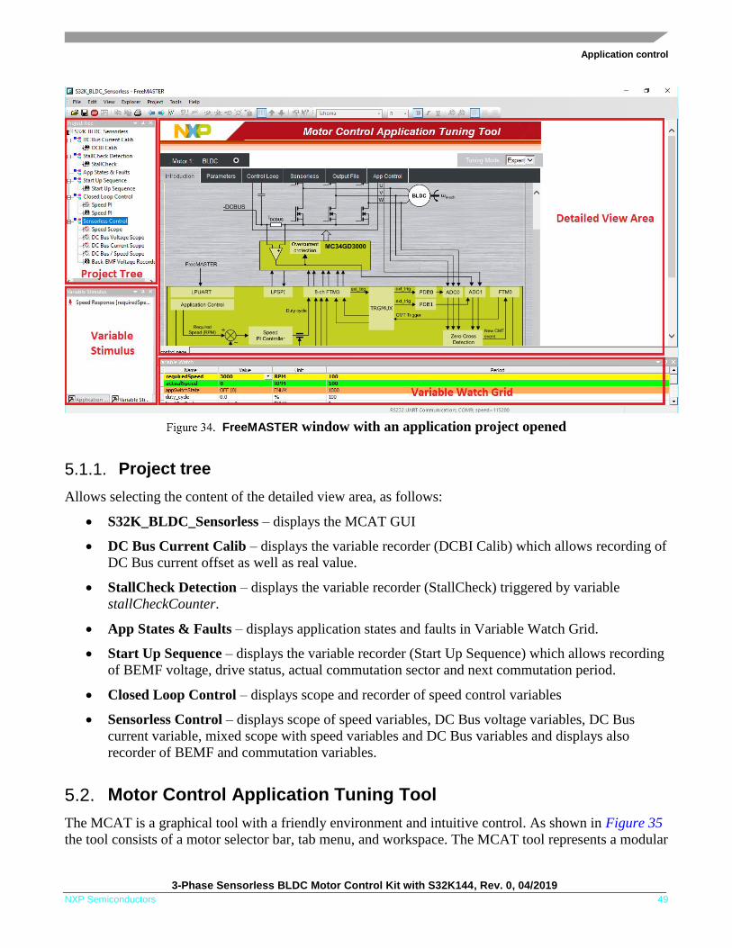
Application control
3-Phase Sensorless BLDC Motor Control Kit with S32K144, Rev. 0, 04/2019
NXP Semiconductors 49
FreeMASTER window with an application project opened
5.1.1. Project tree
Allows selecting the content of the detailed view area, as follows:
• S32K_BLDC_Sensorless – displays the MCAT GUI
• DC Bus Current Calib – displays the variable recorder (DCBI Calib) which allows recording of
DC Bus current offset as well as real value.
• StallCheck Detection – displays the variable recorder (StallCheck) triggered by variable
stallCheckCounter.
• App States & Faults – displays application states and faults in Variable Watch Grid.
• Start Up Sequence – displays the variable recorder (Start Up Sequence) which allows recording
of BEMF voltage, drive status, actual commutation sector and next commutation period.
• Closed Loop Control – displays scope and recorder of speed control variables
• Sensorless Control – displays scope of speed variables, DC Bus voltage variables, DC Bus
current variable, mixed scope with speed variables and DC Bus variables and displays also
recorder of BEMF and commutation variables.
5.2. Motor Control Application Tuning Tool
The MCAT is a graphical tool with a friendly environment and intuitive control. As shown in Figure 35
the tool consists of a motor selector bar, tab menu, and workspace. The MCAT tool represents a modular
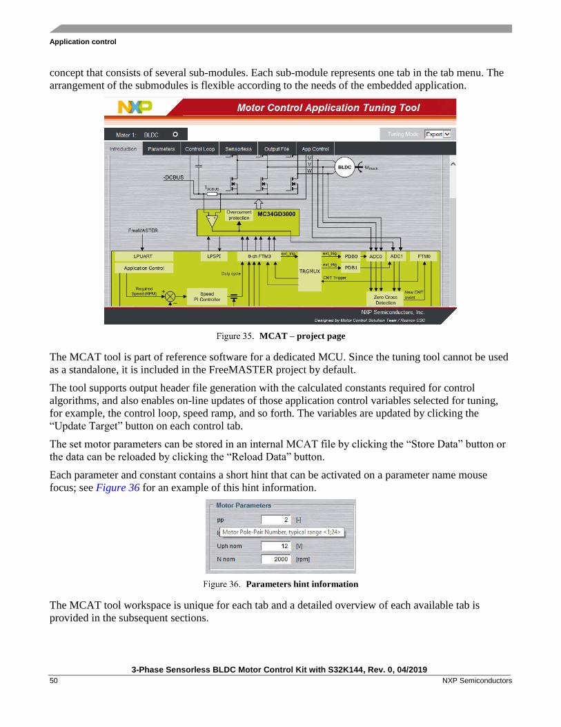
Application control
3-Phase Sensorless BLDC Motor Control Kit with S32K144, Rev. 0, 04/2019
50 NXP Semiconductors
concept that consists of several sub-modules. Each sub-module represents one tab in the tab menu. The
arrangement of the submodules is flexible according to the needs of the embedded application.
MCAT – project page
The MCAT tool is part of reference software for a dedicated MCU. Since the tuning tool cannot be used
as a standalone, it is included in the FreeMASTER project by default.
The tool supports output header file generation with the calculated constants required for control
algorithms, and also enables on-line updates of those application control variables selected for tuning,
for example, the control loop, speed ramp, and so forth. The variables are updated by clicking the
“Update Target” button on each control tab.
The set motor parameters can be stored in an internal MCAT file by clicking the “Store Data” button or
the data can be reloaded by clicking the “Reload Data” button.
Each parameter and constant contains a short hint that can be activated on a parameter name mouse
focus; see Figure 36 for an example of this hint information.
Parameters hint information
The MCAT tool workspace is unique for each tab and a detailed overview of each available tab is
provided in the subsequent sections.
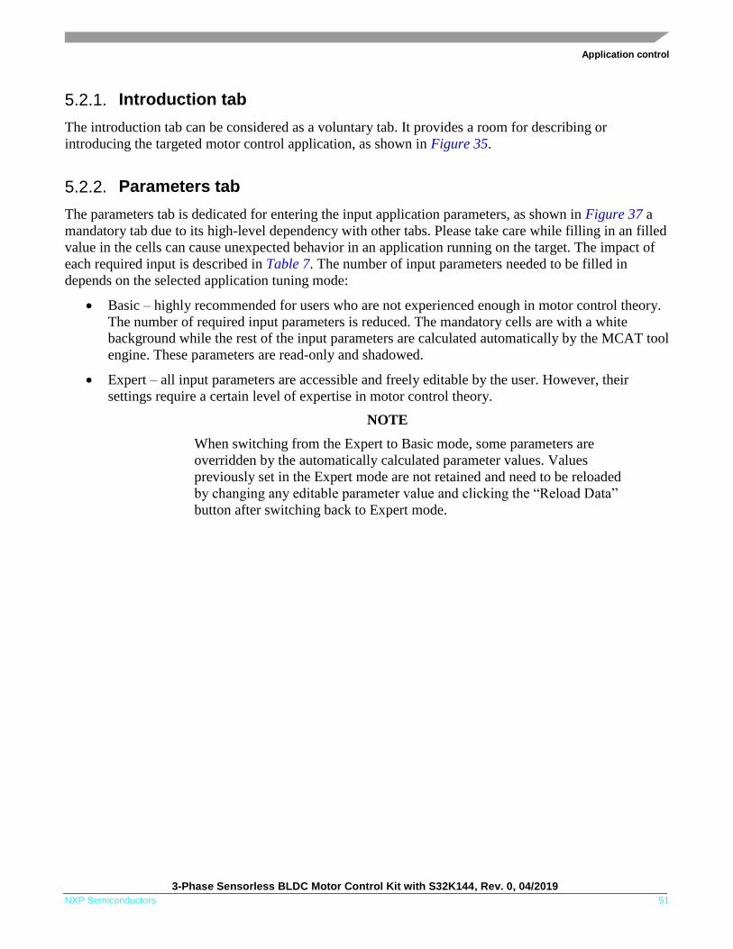
Application control
3-Phase Sensorless BLDC Motor Control Kit with S32K144, Rev. 0, 04/2019
NXP Semiconductors 51
5.2.1. Introduction tab
The introduction tab can be considered as a voluntary tab. It provides a room for describing or
introducing the targeted motor control application, as shown in Figure 35.
5.2.2. Parameters tab
The parameters tab is dedicated for entering the input application parameters, as shown in Figure 37 a
mandatory tab due to its high-level dependency with other tabs. Please take care while filling in an filled
value in the cells can cause unexpected behavior in an application running on the target. The impact of
each required input is described in Table 7. The number of input parameters needed to be filled in
depends on the selected application tuning mode:
• Basic – highly recommended for users who are not experienced enough in motor control theory.
The number of required input parameters is reduced. The mandatory cells are with a white
background while the rest of the input parameters are calculated automatically by the MCAT tool
engine. These parameters are read-only and shadowed.
• Expert – all input parameters are accessible and freely editable by the user. However, their
settings require a certain level of expertise in motor control theory.
NOTE
When switching from the Expert to Basic mode, some parameters are
overridden by the automatically calculated parameter values. Values
previously set in the Expert mode are not retained and need to be reloaded
by changing any editable parameter value and clicking the “Reload Data”
button after switching back to Expert mode.
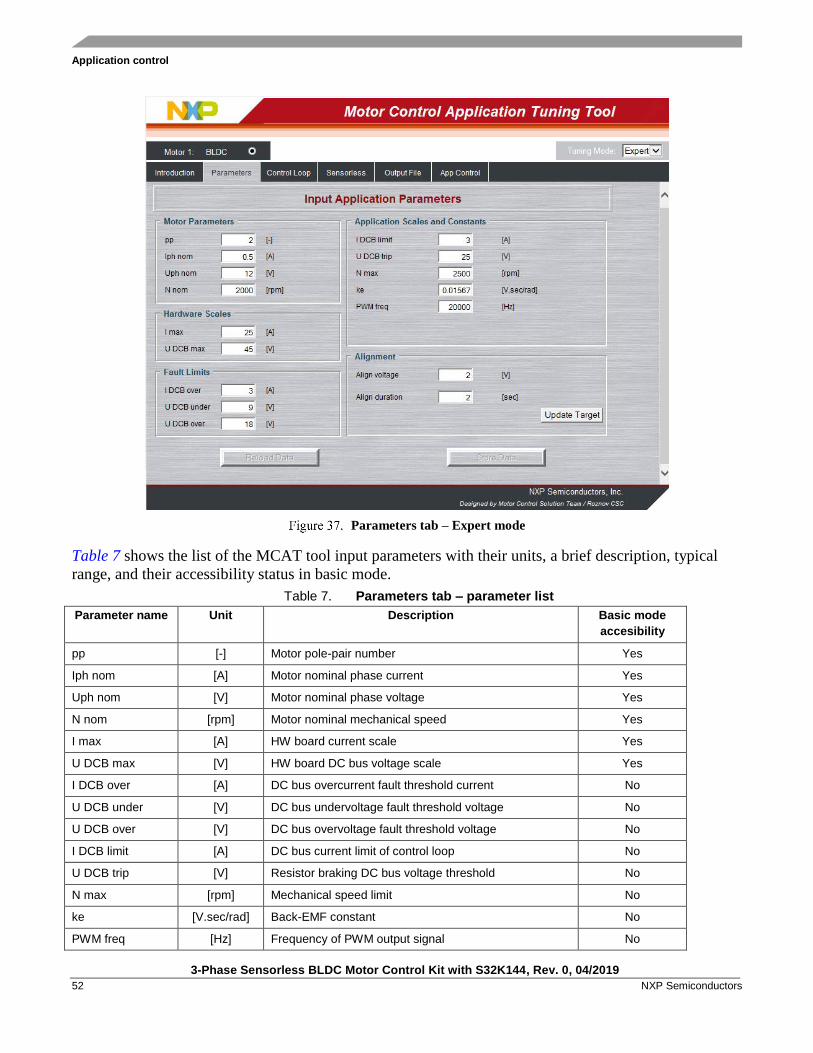
Application control
3-Phase Sensorless BLDC Motor Control Kit with S32K144, Rev. 0, 04/2019
52 NXP Semiconductors
Parameters tab – Expert mode
Table 7 shows the list of the MCAT tool input parameters with their units, a brief description, typical
range, and their accessibility status in basic mode.
Table 7. Parameters tab – parameter list
Parameter name Unit Description Basic mode
accesibility
pp [-] Motor pole-pair number Yes
Iph nom [A] Motor nominal phase current Yes
Uph nom [V] Motor nominal phase voltage Yes
N nom [rpm] Motor nominal mechanical speed Yes
I max [A] HW board current scale Yes
U DCB max [V] HW board DC bus voltage scale Yes
I DCB over [A] DC bus overcurrent fault threshold current No
U DCB under [V] DC bus undervoltage fault threshold voltage No
U DCB over [V] DC bus overvoltage fault threshold voltage No
I DCB limit [A] DC bus current limit of control loop No
U DCB trip [V] Resistor braking DC bus voltage threshold No
N max [rpm] Mechanical speed limit No
ke [V.sec/rad] Back-EMF constant No
PWM freq [Hz] Frequency of PWM output signal No
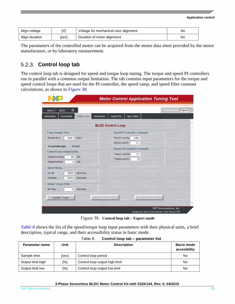
Application control
3-Phase Sensorless BLDC Motor Control Kit with S32K144, Rev. 0, 04/2019
NXP Semiconductors 53
Align voltage [V] Voltage for mechanical rotor alignment No
Align duration [sec] Duration of motor alignment No
The parameters of the controlled motor can be acquired from the motor data sheet provided by the motor
manufacturer, or by laboratory measurement.
5.2.3. Control loop tab
The control loop tab is designed for speed and torque loop tuning. The torque and speed PI controllers
run in parallel with a common output limitation. The tab contains input parameters for the torque and
speed control loops that are used for the PI controller, the speed ramp, and speed filter constant
calculations, as shown in Figure 38.
Control loop tab – Expert mode
Table 8 shows the list of the speed/torque loop input parameters with their physical units, a brief
description, typical range, and their accessibility status in basic mode.
Table 8. Control loop tab – parameter list
Parameter name Unit Description Bacis mode
accesibility
Sample time [sec] Control loop period No
Output limit high [%] Control loop output high limit No
Output limit low [%] Control loop output low limit No
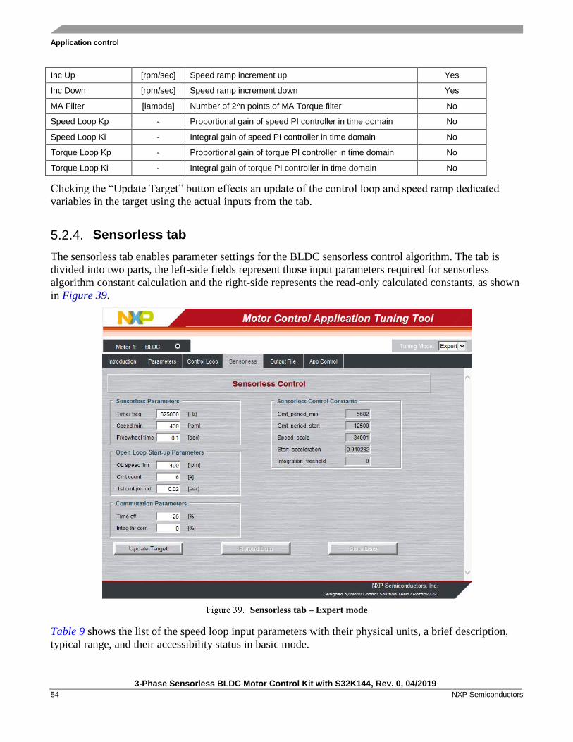
Application control
3-Phase Sensorless BLDC Motor Control Kit with S32K144, Rev. 0, 04/2019
54 NXP Semiconductors
Inc Up [rpm/sec] Speed ramp increment up Yes
Inc Down [rpm/sec] Speed ramp increment down Yes
MA Filter [lambda] Number of 2^n points of MA Torque filter No
Speed Loop Kp - Proportional gain of speed PI controller in time domain No
Speed Loop Ki - Integral gain of speed PI controller in time domain No
Torque Loop Kp - Proportional gain of torque PI controller in time domain No
Torque Loop Ki - Integral gain of torque PI controller in time domain No
Clicking the “Update Target” button effects an update of the control loop and speed ramp dedicated
variables in the target using the actual inputs from the tab.
5.2.4. Sensorless tab
The sensorless tab enables parameter settings for the BLDC sensorless control algorithm. The tab is
divided into two parts, the left-side fields represent those input parameters required for sensorless
algorithm constant calculation and the right-side represents the read-only calculated constants, as shown
in Figure 39.
Sensorless tab – Expert mode
Table 9 shows the list of the speed loop input parameters with their physical units, a brief description,
typical range, and their accessibility status in basic mode.
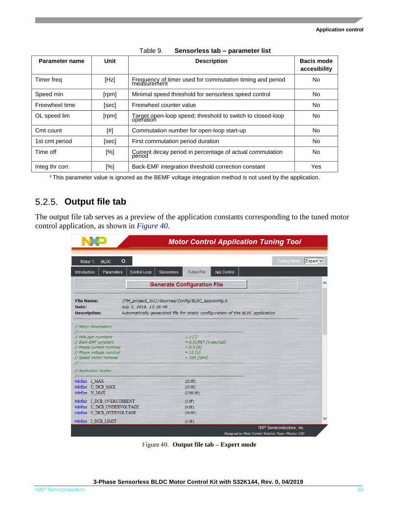
Application control
3-Phase Sensorless BLDC Motor Control Kit with S32K144, Rev. 0, 04/2019
NXP Semiconductors 55
Table 9. Sensorless tab – parameter list
Parameter name Unit Description Bacis mode
accesibility
Timer freq [Hz] Frequency of timer used for commutation timing and period measurement
No
Speed min [rpm] Minimal speed threshold for sensorless speed control No
Freewheel time [sec] Freewheel counter value No
OL speed lim [rpm] Target open-loop speed; threshold to switch to closed-loop operation
No
Cmt count [#] Commutation number for open-loop start-up No
1st cmt period [sec] First commutation period duration No
Time off [%] Current decay period in percentage of actual commutation period
No
Integ thr corr. [%] Back-EMF integration threshold correction constant Yes
1 This parameter value is ignored as the BEMF voltage integration method is not used by the application.
5.2.5. Output file tab
The output file tab serves as a preview of the application constants corresponding to the tuned motor
control application, as shown in Figure 40.
Output file tab – Expert mode
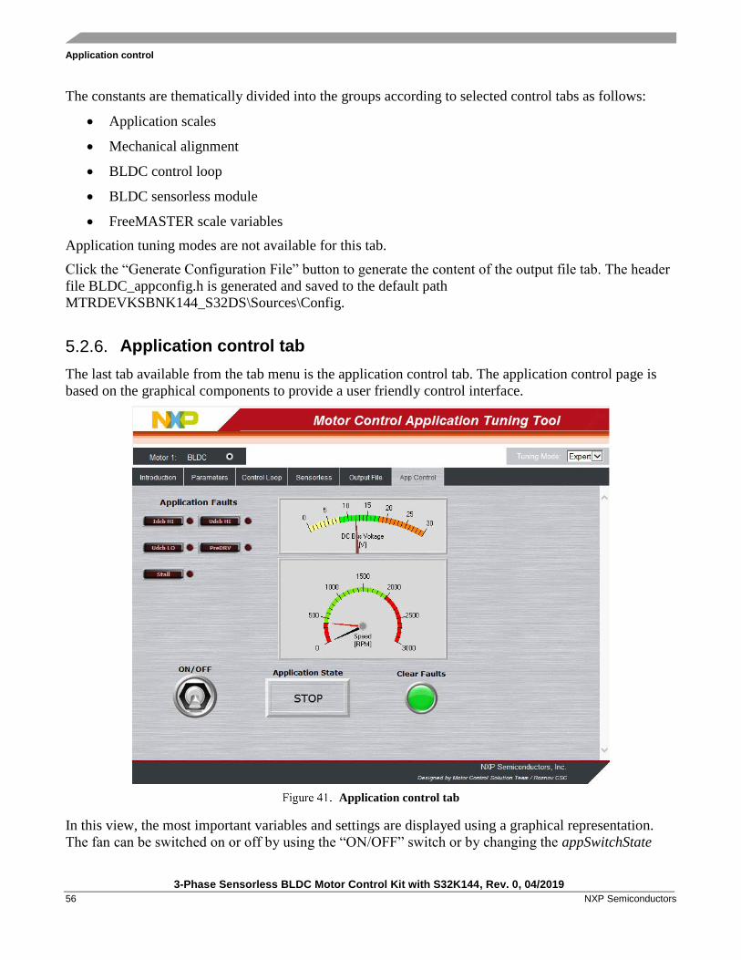
Application control
3-Phase Sensorless BLDC Motor Control Kit with S32K144, Rev. 0, 04/2019
56 NXP Semiconductors
The constants are thematically divided into the groups according to selected control tabs as follows:
• Application scales
• Mechanical alignment
• BLDC control loop
• BLDC sensorless module
• FreeMASTER scale variables
Application tuning modes are not available for this tab.
Click the “Generate Configuration File” button to generate the content of the output file tab. The header
file BLDC_appconfig.h is generated and saved to the default path
MTRDEVKSBNK144_S32DS\Sources\Config.
5.2.6. Application control tab
The last tab available from the tab menu is the application control tab. The application control page is
based on the graphical components to provide a user friendly control interface.
Application control tab
In this view, the most important variables and settings are displayed using a graphical representation.
The fan can be switched on or off by using the “ON/OFF” switch or by changing the appSwitchState
Conclusion
3-Phase Sensorless BLDC Motor Control Kit with S32K144, Rev. 0, 04/2019
NXP Semiconductors 57
variable value in the Variable Watch Grid. The required speed can be selected either by clicking the
speed gauge or by manually changing the requiredSpeed variable value in the Variable Watch Grid.
Where any fault is detected, it has to be cleared manually by clicking the green “Fault Clear” button or
by setting the faultSwitchClear variable value to 0 in the Variable Watch Grid. Then, the application can
be switched on again. Faults present in the system are signalized by the red fault indicators. Pending
faults are signalized by small red circle indicators next to respective fault indicator.
6. Conclusion
The design described shows the simplicity and efficiency in using the S32K144 microcontroller for
Sensorless BLDC motor control and introduces it as an appropriate candidate for various low-cost
applications in the automotive area. MCAT tool provides interactive online tool which makes the BLDC
drive application tuning friendly and intuitive.
References
3-Phase Sensorless BLDC Motor Control Kit with S32K144, Rev. 0, 04/2019
58 NXP Semiconductors
7. References
• MTRDEVKSBNK144: S32K144 Development Kit for sensorless BLDC
• S32 Design Studio IDE for ARM® based MCUs
• FreeMASTER Run-Time Debugging Tool
• S32K14XMCLUG , Automotive Math and Motor Control Library Set for S32K14x User Manual
• S32K1XXRM, S32K1xx Series Reference Manual
• S32K144EVB: S32K144 Evaluation Board
• DEVKIT-MOTORGD: Low-Cost Motor Control Solution for DEVKIT Platform
• GD3000: 3-Phase Brushless Motor Pre-Driver
• Rashid, M. H. Power Electronics Handbook, 2nd Edition. Academic Press
• Motor Control Application Tuning (MCAT) Tool

Document Number: AN12435 Rev. 0
04/2019
How to Reach Us:
Home Page:
nxp.com
Web Support:
nxp.com/support
Information in this document is provided solely to enable system and software
implementers to use NXP products. There are no express or implied copyright licenses
granted hereunder to design or fabricate any integrated circuits based on the
information in this document. NXP reserves the right to make changes without further
notice to any products herein.
NXP makes no warranty, representation, or guarantee regarding the suitability of its
products for any particular purpose, nor does NXP assume any liability arising out of
the application or use of any product or circuit, and specifically disclaims any and all
liability, including without limitation consequential or incidental damages. “Typical”
parameters that may be provided in NXP data sheets and/or specifications can and do
vary in different applications, and actual performance may vary over time. All operating
parameters, including “typicals,” must be validated for each customer application by
customer’s technical experts. NXP does not convey any license under its patent rights
nor the rights of others. NXP sells products pursuant to standard terms and conditions
of sale, which can be found at the following address: nxp.com/SalesTermsandConditions.
While NXP has implemented advanced security features, all products may be subject to
unidentified vulnerabilities. Customers are responsible for the design and operation of
their applications and products to reduce the effect of these vulnerabilities on
customer’s applications and products, and NXP accepts no liability for any vulnerability
that is discovered. Customers should implement appropriate design and operating
safeguards to minimize the risks associated with their applications and products.
NXP, the NXP logo, NXP SECURE CONNECTIONS FOR A SMARTER WORLD,
COOLFLUX, EMBRACE, GREENCHIP, HITAG, I2C BUS, ICODE, JCOP, LIFE VIBES,
MIFARE, MIFARE CLASSIC, MIFARE DESFire, MIFARE PLUS, MIFARE FLEX,
MANTIS, MIFARE ULTRALIGHT, MIFARE4MOBILE, MIGLO, NTAG, ROADLINK,
SMARTLX, SMARTMX, STARPLUG, TOPFET, TRENCHMOS, UCODE, Freescale, the
Freescale logo, AltiVec, C 5, CodeTEST, CodeWarrior, ColdFire, ColdFire+, C Ware,
the Energy Efficient Solutions logo, Kinetis, Layerscape, MagniV, mobileGT, PEG,
PowerQUICC, Processor Expert, QorIQ, QorIQ Qonverge, Ready Play, SafeAssure, the
SafeAssure logo, StarCore, Symphony, VortiQa, Vybrid, Airfast, BeeKit, BeeStack,
CoreNet, Flexis, MXC, Platform in a Package, QUICC Engine, SMARTMOS, Tower,
TurboLink, and UMEMS are trademarks of NXP B.V. All other product or service names
are the property of their respective owners. Arm, AMBA, Arm Powered, Artisan, Cortex,
Jazelle, Keil, SecurCore, Thumb, TrustZone, and μVision are registered trademarks of
Arm Limited (or its subsidiaries) in the EU and/or elsewhere. Arm7, Arm9, Arm11,
big.LITTLE, CoreLink, CoreSight, DesignStart, Mali, Mbed, NEON, POP, Sensinode,
Socrates, ULINK and Versatile are trademarks of Arm Limited (or its subsidiaries) in the
EU and/or elsewhere. All rights reserved. Oracle and Java are registered trademarks of
Oracle and/or its affiliates. The Power Architecture and Power.org word marks and the
Power and Power.org logos and related marks are trademarks and service marks
licensed by Power.org.
© 2019 NXP B.V.
Related Documents