RF Power LDMOS Transistors High Ruggedness N--Channel Enhancement--Mode Lateral MOSFETs RF power transistors designed for both narrowband and broadband ISM, broadcast and aerospace applications operating at frequencies from 1.8 to 2000 MHz. These devices are fabricated using NXP’s enhanced ruggedness platform and are suitable for use in applications where high VSWRs are encountered. Typical Performance: V DD = 50 Volts Frequency (MHz) Signal Type P out (W) G ps (dB) D (%) IMD (1) (dBc) 1.8 to 30 (2,6) Two--Tone (10 kHz spacing) 25 PEP 25 51 --30 30--512 (3,6) Two--Tone (200 kHz spacing) 25 PEP 17.1 30.1 --32 512 (4) Pulse (100 sec, 20% Duty Cycle) 25 Peak 25.4 74.5 — 512 (4) CW 25 25.5 74.7 — 1030 (5) CW 25 22.5 60 — Load Mismatch/Ruggedness Frequency (MHz) Signal Type VSWR P in (W) Test Voltage Result 30 (2) CW >65:1 at all Phase Angles 0.23 (3 dB Overdrive) 50 No Device Degradation 512 (3) CW 1.6 (3 dB Overdrive) 512 (4) Pulse (100 sec, 20% Duty Cycle) 0.14 Peak (3 dB Overdrive) 512 (4) CW 0.14 (3 dB Overdrive 1030 (5) CW 0.34 (3 dB Overdrive 1. Distortion products are referenced to one of two tones. See p. 13, 20. 2. Measured in 1.8--30 MHz broadband reference circuit. 3. Measured in 30--512 MHz broadband reference circuit. 4. Measured in 512 MHz narrowband test circuit. 5. Measured in 1030 MHz narrowband test circuit. 6. The values shown are the minimum measured performance numbers across the in- dicated frequency range. Features Wide operating frequency range Extreme ruggedness Unmatched, capable of very broadband operation Integrated stability enhancements Low thermal resistance Extended ESD protection circuit Document Number: MRFE6VS25N Rev. 2, 03/2019 NXP Semiconductors Technical Data 1.8--2000 MHz, 25 W, 50 V WIDEBAND RF POWER LDMOS TRANSISTORS MRFE6VS25NR1 MRFE6VS25GNR1 Note: The backside of the package is the source terminal for the transistor. Figure 1. Pin Connections TO--270--2 PLASTIC MRFE6VS25NR1 TO--270G--2 PLASTIC MRFE6VS25GNR1 (Top View) Drain 2 1 Gate 2012, 2019 NXP B.V .

Welcome message from author
This document is posted to help you gain knowledge. Please leave a comment to let me know what you think about it! Share it to your friends and learn new things together.
Transcript
MRFE6VS25NR1 MRFE6VS25GNR1
1RF Device DataNXP Semiconductors
RF Power LDMOS TransistorsHigh Ruggedness N--ChannelEnhancement--Mode Lateral MOSFETsRF power transistors designed for both narrowband and broadband ISM,
broadcast and aerospace applications operating at frequencies from 1.8 to2000 MHz. These devices are fabricated using NXP’s enhanced ruggednessplatform and are suitable for use in applications where high VSWRs areencountered.
Typical Performance: VDD = 50 Volts
Frequency(MHz) Signal Type
Pout(W)
Gps(dB)
D(%)
IMD (1)
(dBc)
1.8 to 30 (2,6) Two--Tone(10 kHz spacing)
25 PEP 25 51 --30
30--512 (3,6) Two--Tone(200 kHz spacing)
25 PEP 17.1 30.1 --32
512 (4) Pulse (100 sec,20% Duty Cycle)
25 Peak 25.4 74.5 —
512 (4) CW 25 25.5 74.7 —
1030 (5) CW 25 22.5 60 —
Load Mismatch/Ruggedness
Frequency(MHz) Signal Type VSWR
Pin(W)
TestVoltage Result
30 (2) CW >65:1at all PhaseAngles
0.23(3 dB
Overdrive)
50 No DeviceDegradation
512 (3) CW 1.6(3 dB
Overdrive)
512 (4) Pulse(100 sec, 20%Duty Cycle)
0.14 Peak(3 dB
Overdrive)
512 (4) CW 0.14(3 dB
Overdrive
1030 (5) CW 0.34(3 dB
Overdrive
1. Distortion products are referenced to one of two tones. See p. 13, 20.2. Measured in 1.8--30 MHz broadband reference circuit.3. Measured in 30--512 MHz broadband reference circuit.4. Measured in 512 MHz narrowband test circuit.5. Measured in 1030 MHz narrowband test circuit.6. The values shown are theminimummeasured performance numbers across the in-
dicated frequency range.
Features
Wide operating frequency range Extreme ruggedness Unmatched, capable of very broadband operation Integrated stability enhancements Low thermal resistance Extended ESD protection circuit
Document Number: MRFE6VS25NRev. 2, 03/2019
NXP SemiconductorsTechnical Data
1.8--2000 MHz, 25 W, 50 VWIDEBAND
RF POWER LDMOS TRANSISTORS
MRFE6VS25NR1MRFE6VS25GNR1
Note: The backside of the package is thesource terminal for the transistor.
Figure 1. Pin Connections
TO--270--2PLASTIC
MRFE6VS25NR1
TO--270G--2PLASTIC
MRFE6VS25GNR1
(Top View)
Drain2 1Gate
2012, 2019 NXP B.V.
2RF Device Data
NXP Semiconductors
MRFE6VS25NR1 MRFE6VS25GNR1
Table 1. Maximum Ratings
Rating Symbol Value Unit
Drain--Source Voltage VDSS --0.5, +133 Vdc
Gate--Source Voltage VGS --6.0, +10 Vdc
Storage Temperature Range Tstg --65 to +150 C
Case Operating Temperature TC --40 to +150 C
Operating Junction Temperature (1,2) TJ --40 to +225 C
Table 2. Thermal Characteristics
Characteristic Symbol Value (2,3) Unit
Thermal Resistance, Junction to CaseCW: Case Temperature 80C, 25 W CW, 50 Vdc, IDQ = 10 mA, 512 MHz
RJC 1.2 C/W
Thermal Impedance, Junction to CasePulse: Case Temperature 77C, 25 W Peak, 100 sec Pulse Width,20% Duty Cycle, 50 Vdc, IDQ = 10 mA, 512 MHz
ZJC 0.29 C/W
Table 3. ESD Protection Characteristics
Test Methodology Class
Human Body Model (per JESD22--A114) 2, passes 2500 V
Machine Model (per EIA/JESD22--A115) B, passes 250 V
Charge Device Model (per JESD22--C101) IV, passes 2000 V
Table 4. Moisture Sensitivity Level
Test Methodology Rating Package Peak Temperature Unit
Per JESD22--A113, IPC/JEDEC J--STD--020 3 260 C
Table 5. Electrical Characteristics (TA = 25C unless otherwise noted)
Characteristic Symbol Min Typ Max Unit
Off Characteristics
Gate--Source Leakage Current(VGS = 5 Vdc, VDS = 0 Vdc)
IGSS — — 400 nAdc
Drain--Source Breakdown Voltage(VGS = 0 Vdc, ID = 50 mA)
V(BR)DSS 133 142 — Vdc
Zero Gate Voltage Drain Leakage Current(VDS = 50 Vdc, VGS = 0 Vdc)
IDSS — — 2 Adc
Zero Gate Voltage Drain Leakage Current(VDS = 100 Vdc, VGS = 0 Vdc)
IDSS — — 7 Adc
On Characteristics
Gate Threshold Voltage(VDS = 10 Vdc, ID = 85 Adc)
VGS(th) 1.5 2.0 2.5 Vdc
Gate Quiescent Voltage(VDD = 50 Vdc, ID = 10 mAdc, Measured in Functional Test)
VGS(Q) 2.0 2.4 3.0 Vdc
Drain--Source On--Voltage(VGS = 10 Vdc, ID = 210 mAdc)
VDS(on) — 0.28 — Vdc
Dynamic Characteristics
Reverse Transfer Capacitance(VDS = 50 Vdc 30 mV(rms)ac @ 1 MHz, VGS = 0 Vdc)
Crss — 0.26 — pF
Output Capacitance(VDS = 50 Vdc 30 mV(rms)ac @ 1 MHz, VGS = 0 Vdc)
Coss — 14.2 — pF
Input Capacitance(VDS = 50 Vdc, VGS = 0 Vdc 30 mV(rms)ac @ 1 MHz)
Ciss — 39.2 — pF
1. Continuous use at maximum temperature will affect MTTF.2. MTTF calculator available at http://www.nxp.com/RF/calculators.3. Refer to AN1955, Thermal Measurement Methodology of RF Power Amplifiers. Go to http://www.nxp.com/RF and search for AN1955.
(continued)
MRFE6VS25NR1 MRFE6VS25GNR1
3RF Device DataNXP Semiconductors
Table 5. Electrical Characteristics (TA = 25C unless otherwise noted) (continued)
Characteristic Symbol Min Typ Max Unit
Functional Tests (1) (In NXP Test Fixture, 50 ohm system) VDD = 50 Vdc, IDQ = 10 mA, Pout = 25 W Peak (5 W Avg.), f = 512 MHz,100 sec Pulse Width, 20% Duty Cycle
Power Gain Gps 24.0 25.4 27.0 dB
Drain Efficiency D 70.0 74.5 — %
Input Return Loss IRL — --16 --10 dB
Load Mismatch/Ruggedness (In NXP Test Fixture, 50 ohm system) IDQ = 10 mA
Frequency(MHz)
SignalType VSWR
Pin(W) Test Voltage, VDD Result
512 Pulse(100 sec, 20% Duty Cycle)
>65:1at all Phase Angles
0.14 Peak(3 dB Overdrive)
50 No Device Degradation
CW 0.14(3 dB Overdrive)
Table 6. Ordering Information
Device Shipping Information Package
MRFE6VS25NR1R1 Suffix = 500 Units, 24 mm Tape Width, 13--Inch Reel
TO--270--2
MRFE6VS25GNR1 TO--270G--2
1. Measurements made with device in straight lead configuration before any lead forming operation is applied. Lead forming is used for gull wing(GN) parts.
4RF Device Data
NXP Semiconductors
MRFE6VS25NR1 MRFE6VS25GNR1
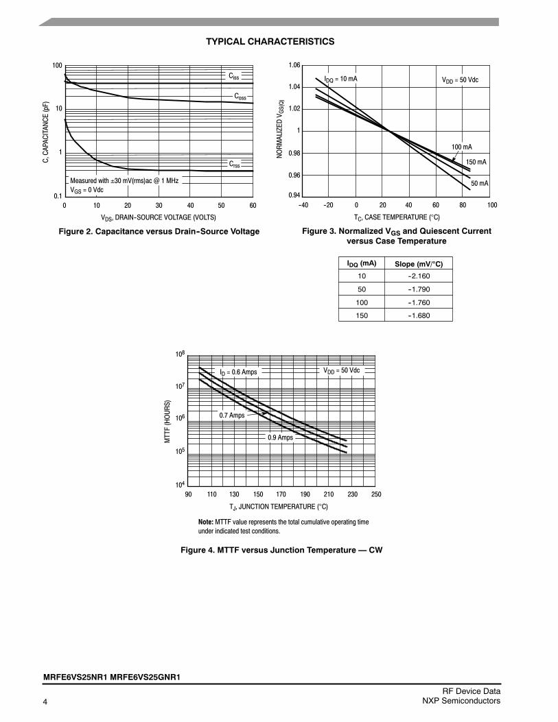
TYPICAL CHARACTERISTICS
600.1
100
0 2010
VDS, DRAIN--SOURCE VOLTAGE (VOLTS)
Figure 2. Capacitance versus Drain--Source Voltage
C,CAPACITANCE(pF)
30
Ciss
10
1
Coss
Crss
Measured with 30 mV(rms)ac @ 1 MHzVGS = 0 Vdc
IDQ = 10 mA
Figure 3. Normalized VGS and Quiescent Currentversus Case Temperature
NORMALIZED
V GS(Q)
TC, CASE TEMPERATURE (C)
1.06
1.04
1.02
1
0.98
0.96
0.94100--40 0--20 20 40 60
VDD = 50 Vdc
250
108
90
TJ, JUNCTION TEMPERATURE (C)
107
106
104
110 130 150 170 190
MTTF(HOURS)
210 230
105
ID = 0.6 Amps
0.7 Amps
0.9 Amps
150 mA
VDD = 50 Vdc
40 50 80
100 mA
50 mA
Figure 4. MTTF versus Junction Temperature — CW
Note: MTTF value represents the total cumulative operating timeunder indicated test conditions.
10
IDQ (mA) Slope (mV/C)
50
100
150
--2.160
--1.790
--1.760
--1.680

MRFE6VS25NR1 MRFE6VS25GNR1
5RF Device DataNXP Semiconductors
512 MHz NARROWBAND PRODUCTION TEST FIXTURE
Figure 5. MRFE6VS25NR1 Narrowband Test Circuit Component Layout — 512 MHz
MRFE6VS25NRev. 1
CUTOUTAREA
C1
B1
C2 C3
L1
C4
C8C7
C5*
C6
C9*
C10* C11
C12
C15
B2
L3
L2
C13C14
*C5, C9 and C10 are mounted vertically.
Table 7. MRFE6VS25NR1 Narrowband Test Circuit Component Designations and Values — 512 MHzPart Description Part Number Manufacturer
B1, B2 Long Ferrite Beads 2743021447 Fair-Rite
C1 22 F, 35 V Tantalum Capacitor T491X226K035AT Kemet
C2, C13 0.1 F Chip Capacitors CDR33BX104AKWY AVX
C3, C14 0.01 F Chip Capacitors C0805C103K5RAC Kemet
C4, C11, C12 180 pF Chip Capacitors ATC100B181JT300XT ATC
C5 18 pF Chip Capacitor ATC100B180JT500XT ATC
C6 2.7 pF Chip Capacitor ATC100B2R7BT500XT ATC
C7 15 pF Chip Capacitor ATC100B150JT500XT ATC
C8 36 pF Chip Capacitor ATC100B360JT500XT ATC
C9 4.3 pF Chip Capacitor ATC100B4R3CT500XT ATC
C10 13 pF Chip Capacitor ATC100B130JT500XT ATC
C15 470 F, 63 V Electrolytic Capacitor MCGPR63V477M13X26-RH Multicomp
L1 33 nH Inductor 1812SMS-33NJLC Coilcraft
L2 12.5 nH Inductor A04TJLC Coilcraft
L3 82 nH Inductor 1812SMS-82NJLC Coilcraft
PCB 0.030, r = 2.55 AD255A Arlon
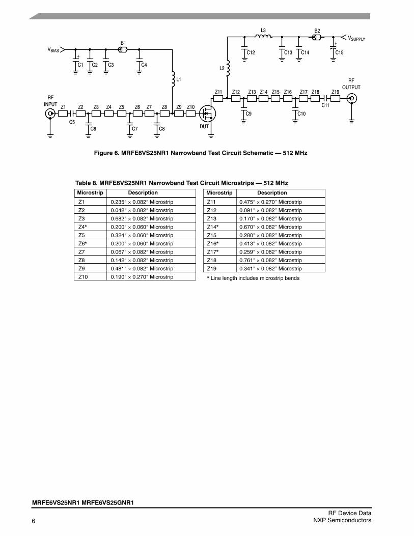
6RF Device Data
NXP Semiconductors
MRFE6VS25NR1 MRFE6VS25GNR1
Z1 0.235 0.082 Microstrip
Z2 0.042 0.082 Microstrip
Z3 0.682 0.082 Microstrip
Z4* 0.200 0.060 Microstrip
Z5 0.324 0.060 Microstrip
Z6* 0.200 0.060 Microstrip
Z7 0.067 0.082 Microstrip
Z8 0.142 0.082 Microstrip
Z9 0.481 0.082 Microstrip
Z10 0.190 0.270 Microstrip
Z11 0.475 0.270 Microstrip
Z12 0.091 0.082 Microstrip
Z13 0.170 0.082 Microstrip
Z14* 0.670 0.082 Microstrip
Z15 0.280 0.082 Microstrip
Z16* 0.413 0.082 Microstrip
Z17* 0.259 0.082 Microstrip
Z18 0.761 0.082 Microstrip
Z19 0.341 0.082 Microstrip
* Line length includes microstrip bends
Table 8. MRFE6VS25NR1 Narrowband Test Circuit Microstrips — 512 MHz
DescriptionMicrostrip DescriptionMicrostrip
Figure 6. MRFE6VS25NR1 Narrowband Test Circuit Schematic — 512 MHz
Z1
RFINPUT
C5
Z2 Z4
DUT
C11
RFOUTPUT
VBIAS
VSUPPLY
C2
C13 C15
+
Z16
Z3 Z5
C3
Z15Z14Z13Z12Z11
Z10Z8Z7Z6
C1
Z17 Z18
C14
C6 C7 C8
L1
B1
+
C4
Z9
L2
C9 C10
Z19
B2L3
C12

MRFE6VS25NR1 MRFE6VS25GNR1
7RF Device DataNXP Semiconductors
TYPICAL CHARACTERISTICS — 512 MHz
Pin, INPUT POWER (dBm)
40
35
30
25
P out,OUTPUTPOWER
(dBm
)
45
15 20
50
20
15
25
0 105
512 27.8 31.4
f(MHz)
P1dB(W)
P3dB(W)
0
VGS, GATE--SOURCE VOLTAGE (VOLTS)
Figure 7. CW Output Power versus Gate--SourceVoltage at a Constant Input Power
0
35
30
P out,OUTPUTPOWER
(WATTS)
15
10
5
2 3 4
VDD = 50 VdcPin = 0.07 Wf = 512 MHz
Figure 8. CW Output Power versus Input Power
19
27
0.310
90
1
25
23
70
60
50
40
30
Pout, OUTPUT POWER (WATTS)
Figure 9. Power Gain and Drain Efficiencyversus CW Output Power
Gps,POWER
GAIN(dB)
D,DRAINEFFICIENCY(%)
26
24
22
10 50
25_C
TC = --30_C
85_C
85_C
VDD = 50 VdcIDQ = 10 mAf = 512 MHz
25_C
--30_C
21
20
25
20
1
Gps
VDD = 50 VdcIDQ = 10 mAf = 512 MHz
20
80
D

8RF Device Data
NXP Semiconductors
MRFE6VS25NR1 MRFE6VS25GNR1
512 MHz NARROWBAND PRODUCTION TEST FIXTURE
VDD = 50 Vdc, IDQ = 10 mA, Pout = 25 W Peak
fMHz
Zsource
Zload
512 1.56 + j11.6 9.5 + j18.3
Zsource = Test circuit impedance as measured fromgate to ground.
Zload = Test circuit impedance as measured fromdrain to ground.
Figure 10. Narrowband Series Equivalent Source and Load Impedance — 512 MHz
InputMatchingNetwork
DeviceUnderTest
OutputMatchingNetwork
Zsource Zload
5050

MRFE6VS25NR1 MRFE6VS25GNR1
9RF Device DataNXP Semiconductors
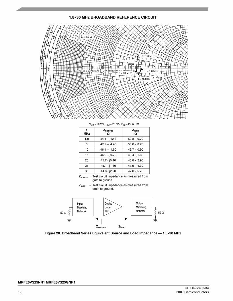
1.8--30 MHz BROADBAND REFERENCE CIRCUIT
Table 9. 1.8--30 MHz Broadband Performance (In NXP Reference Circuit, 50 ohm system)VDD = 50 Volts, IDQ = 100 mA
Signal TypePout(W)
f(MHz)
Gps(dB)
D(%)
IMD(dBc)
Two-Tone(10 kHz spacing)
25 PEP 1.8 25.7 51.5 --30.7
10 25.8 50.7 --34.8
30 24.8 50.7 --33.0
Table 10. Load Mismatch/Ruggedness (In NXP Reference Circuit)
Frequency(MHz) Signal Type VSWR
Pin(W) Test Voltage, VDD Result
30 CW >65:1at all PhaseAngles
0.23(3 dB Overdrive)
50 No DeviceDegradation

10RF Device Data
NXP Semiconductors
MRFE6VS25NR1 MRFE6VS25GNR1
1.8--30 MHz BROADBAND REFERENCE CIRCUIT
Figure 11. MRFE6VS25NR1 Broadband Reference Circuit Component Layout — 1.8--30 MHz
+
MRFE6VS25L/NRev. 0
CUTOUTAREA
C3
*C1 and C11 are mounted vertically.
C2
C4 C5
E1, L1
C1*
R1
C9
Q1
E2, L2 C11*
C10
C8C7C6
Table 11. MRFE6VS25NR1 Broadband Reference Circuit Component Designations and Values — 1.8--30 MHzPart Description Part Number Manufacturer
C1, C5, C6, C9, C11 20K pF Chip Capacitors ATC200B203KT50XT ATC
C2 10 F, 35 V Tantalum Capacitor T491D106K035AT Kemet
C3 0.1 F Chip Capacitor CDR33BX104AKWY AVX
C4 2.2 F Chip Capacitor C3225X7R1H225KT TDK
C7 0.1 F Chip Capacitor GRM319R72A104KA01D Murata
C8 2.2 F Chip Capacitor G2225X7R225KT3AB ATC
C10 220 F, 100 V Electolytic Capacitor MCGPR100V227M16X26-RH Multicomp
E1 #43 Ferrite Toroid 5943001101 Fair--Rite
E2 #61 Ferrite Toroid 5961001101 Fair--Rite
L1 4 Turns, 22 AWG, Toroid Transformer with Ferrite E1 8077 Copper Magnetic Wire Belden
L2 26 Turns, 22 AWG, Toroid Transformer with Ferrite E2 8077 Copper Magnetic Wire Belden
Q1 RF Power LDMOS Transistor MRFE6VS25NR1 NXP
R1 1 k, 3 W Axial Leaded Resistor CPF31K0000FKE14 Vishay
PCB 0.030, r = 4.8 S1000 Shenzhen MultilayerPCB Technology

MRFE6VS25NR1 MRFE6VS25GNR1
11RF Device DataNXP Semiconductors
Z1, Z10 0.141 0.047 Microstrip
Z2, Z9 0.625 0.047 Microstrip
Z3 0.119 0.219 Microstrip
Z4, Z8 0.422 0.241 Microstrip
Z5, Z6 0.469 0.263 Microstrip
Z7 0.119 0.063 Microstrip
Table 12. MRFE6VS25NR1 Broadband Reference Test Circuit Microstrips — 1.8--30 MHz
DescriptionMicrostrip DescriptionMicrostrip
Figure 12. MRFE6VS25NR1 Broadband Reference Circuit Schematic — 1.8--30 MHz
Z1
RFINPUT
C1
Z2
DUT
C11
RFOUTPUT
VBIAS
VSUPPLYC3
C7 C10
+
Z5
C4
Z6
C2
Z9
C8
+
C5
Z10
E1, L1
Z3
Z4 R1
Z8
C9
Z7E2, L2
C6

12RF Device Data
NXP Semiconductors
MRFE6VS25NR1 MRFE6VS25GNR1
TYPICAL CHARACTERISTICS — 1.8--30 MHzBROADBAND REFERENCE CIRCUIT
Pin, INPUT POWER (dBm)
38
42
P out,OUTPUTPOWER
(dBm
)
40
44
46
3612 14
f = 10 MHz
16 18 24 28
VDD = 50 VdcIDQ = 25 mA
20 22 26
P out,OUTPUT
POWER
(WATTS)
D,DRAIN
EFFICIENCY(%)
0
Gps
f, FREQUENCY (MHz)
Figure 13. Power Gain, CW Output Power and DrainEfficiency versus Frequency at a Constant Input Power
20
28
27
22
75
69
66
26
24
D
Gps,POWER
GAIN(dB)
26
25
24
21
5 10 15 30
63
VDD = 50 Vdc, Pin = 0.1 WIDQ = 25 mA
Pout
23
22
20 25
28
0
VGS, GATE--SOURCE VOLTAGE (VOLTS)
Figure 14. CW Output Power versus Gate--SourceVoltage at a Constant Input Power
0
35
30
P out,OUTPUTPOWER
(WATTS)
20
10
0.5 1 2.5 31.5 2 3.5
VDD = 50 VdcPin = 0.1 W
30 MHz
72
25
15
5
f = 10 MHz
1.8 MHz
Figure 15. CW Output Power versus Input Power
1.8
10
30
23
25
25
28
30
30
f(MHz)
P1dB(W)
P3dB(W)
18
26
510
90
10
24
22
60
50
40
30
20
Pout, OUTPUT POWER (WATTS)
Figure 16. Power Gain and Drain Efficiency versus CW Output Power
Gps,POWER
GAIN(dB)
D,DRAINEFFICIENCY(%)
23
21
20
30 35
25
70Gps
VDD = 50 VdcIDQ = 25 mA
D
10 MHz
19
15 20 25
80
10 MHz
1.8 MHz
30 MHz
1.8 MHz
30 MHz
30 MHz
1.8 MHz

MRFE6VS25NR1 MRFE6VS25GNR1
13RF Device DataNXP Semiconductors
TYPICAL CHARACTERISTICS — 1.8--30 MHzBROADBAND REFERENCE CIRCUIT — TWO--TONE (1)
Figure 17. Intermodulation DistortionProducts versus Output Power — 1.8 MHz
--70
--20
10
7th Order
Pout, OUTPUT POWER (WATTS) PEP
VDD = 50 Vdc, IDQ = 100 mAf1 = 1.795 MHz, f2 = 1.805 MHzTwo--Tone Measurements
3rd Order
--30
--40
--50
30
IMD,INTERMODULATIONDISTORTION(dBc)
--60
5th Order
2
Figure 18. Intermodulation DistortionProducts versus Output Power — 10 MHz
--60
--25
10
7th Order
Pout, OUTPUT POWER (WATTS) PEP
3rd Order
--30
--40
--50
30
IMD,INTERMODULATIONDISTORTION(dBc)
--55
5th Order
2
Figure 19. Intermodulation DistortionProducts versus Output Power — 30 MHz
--60
--25
10
7th Order
Pout, OUTPUT POWER (WATTS) PEP
VDD = 50 Vdc, IDQ = 100 mAf1 = 29.995 MHz, f2 = 30.005 MHzTwo--Tone Measurements
3rd Order
--30
--35
--40
30
IMD,INTERMODULATIONDISTORTION(dBc)
--50 5th Order
2
VDD = 50 Vdc, IDQ = 100 mAf1 = 9.995 MHz, f2 = 10.005 MHzTwo--Tone Measurements
--45
--35
--55
--45
1. The distortion products are referenced to one of the two tones and the peak envelope power (PEP) is 6 dB above the power in a single tone.
14RF Device Data
NXP Semiconductors
MRFE6VS25NR1 MRFE6VS25GNR1
1.8--30 MHz BROADBAND REFERENCE CIRCUIT
Zo = 50
Zsource
Zload
f = 30 MHz
f = 1.8 MHz
f = 1.8 MHz
f = 30 MHz
VDD = 50 Vdc, IDQ = 25 mA, Pout = 25 W CW
fMHz
Zsource
Zload
1.8 44.4 + j12.8 50.8 - j0.70
5 47.2 + j4.40 50.0 - j0.70
10 46.4 + j1.50 49.7 - j0.90
15 46.0 + j0.70 49.4 - j1.60
20 45.7 - j0.40 48.8 - j2.90
25 45.1 - j1.60 47.9 - j4.30
30 44.6 - j2.90 47.0 - j5.70
Zsource = Test circuit impedance as measured fromgate to ground.
Zload = Test circuit impedance as measured fromdrain to ground.
Figure 20. Broadband Series Equivalent Source and Load Impedance — 1.8--30 MHz
InputMatchingNetwork
DeviceUnderTest
OutputMatchingNetwork
Zsource Zload
5050
MRFE6VS25NR1 MRFE6VS25GNR1
15RF Device DataNXP Semiconductors
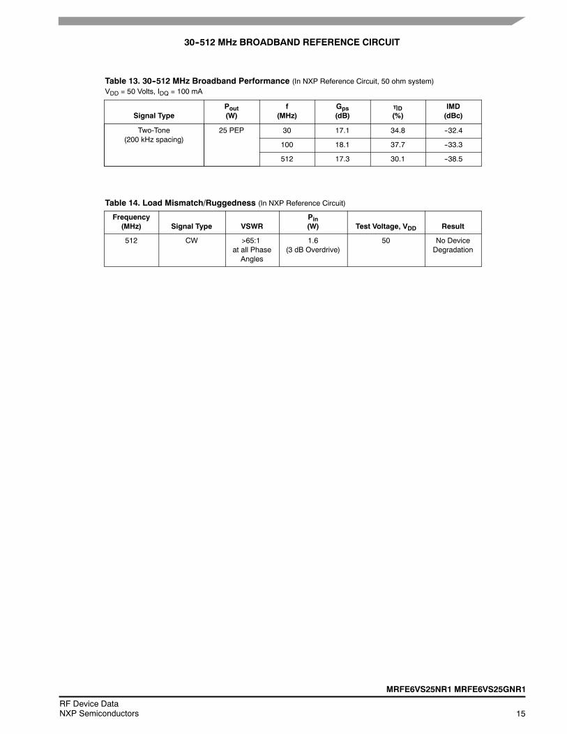
30--512 MHz BROADBAND REFERENCE CIRCUIT
Table 13. 30--512 MHz Broadband Performance (In NXP Reference Circuit, 50 ohm system)VDD = 50 Volts, IDQ = 100 mA
Signal TypePout(W)
f(MHz)
Gps(dB)
D(%)
IMD(dBc)
Two-Tone(200 kHz spacing)
25 PEP 30 17.1 34.8 --32.4
100 18.1 37.7 --33.3
512 17.3 30.1 --38.5
Table 14. Load Mismatch/Ruggedness (In NXP Reference Circuit)
Frequency(MHz) Signal Type VSWR
Pin(W) Test Voltage, VDD Result
512 CW >65:1at all PhaseAngles
1.6(3 dB Overdrive)
50 No DeviceDegradation

16RF Device Data
NXP Semiconductors
MRFE6VS25NR1 MRFE6VS25GNR1
30--512 MHz BROADBAND REFERENCE CIRCUIT
Figure 21. MRFE6VS25NR1 Broadband Reference Circuit Component Layout — 30--512 MHz
MRFE6VS25L/NRev. 0
D1 C5
R3
C7
L1
R2C2
C1 C3
E1
Q1
E4
C4
E3
T2
T3T1
E2, L2C11
C10
C9
C8R1
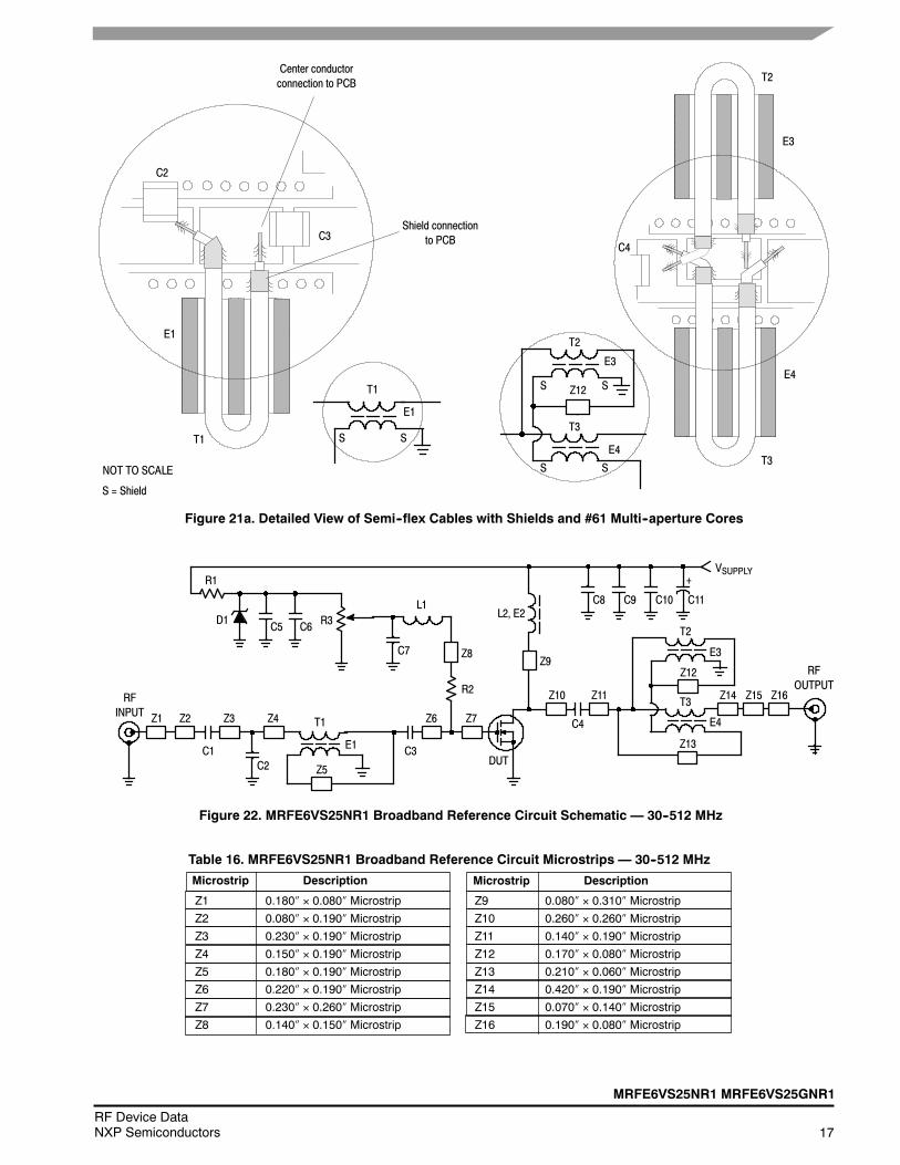
Note: See Figure 21a for a more detailed view of the semi--flex cables with shields and #61 multi--aperture cores.
C6
Table 15. MRFE6VS25NR1 Broadband Reference Circuit Component Designations and Values — 30--512 MHzPart Description Part Number Manufacturer
C1, C3, C6, C7, C8 1,000 pF Chip Capacitors ATC100B102JT50XT ATC
C2 2.7 pF Chip Capacitor ATC100B2R7BT500XT ATC
C4 15 nF Chip Capacitor C3225CH2A153JT TDK
C5, C9 10 nF Chip Capacitors GRM3195C1E103JA01 Murata
C10 1 F Chip Capacitor C3225JB2A105KT TDK
C11 220 F, 100 V Electrolytic Capacitor MCGPR100V227M16X26-RH Multicomp
D1 8.2 V, 1 W Zener Diode 1N4738A Fairchild Semiconductor
E1, E3, E4 #61 Multi-aperture Cores 2861001502 Fair-Rite
E2 Ferrite Core Bead 21-201-J Ferronics
L1 47 nH Inductor 1812SMS-47NJLC Coilcraft
L2 4 Turns, 20 AWG, Toroid Transformer withFerrite E2
8076 Copper Magnetic Wire Belden
Q1 RF Power LDMOS Transistor MRFE6VS25NR1 NXP
R1 5.6 k, 1/4 W Chip Resistor CRCW12065K60FKEA Vishay
R2 15 , 1/4 W Chip Resistor CRCW120615R0FKEA Vishay
R3 5 k Potentiometer CMS Cermet Multi--turn 3224W-1-502E Bourns
T1 25 Semi-flex Cable, 0.945 Shield Length D260-4118-0000 Microdot
T2, T3 25 Semi-flex Cables, 1.340 Shield Length D260-4118-0000 Microdot
PCB 0.030, r = 3.5 TC350 Arlon
MRFE6VS25NR1 MRFE6VS25GNR1
17RF Device DataNXP Semiconductors
Figure 21a. Detailed View of Semi--flex Cables with Shields and #61 Multi--aperture Cores
NOT TO SCALE
Center conductorconnection to PCB
Shield connectionto PCB
C2
C3
E1
T1
E4
T3
E3
T2
C4
T1
E1
T2
T3
E3
E4
Z12
ST3
S = Shield
S
S S
S S
Z1 0.180 0.080 Microstrip
Z2 0.080 0.190 Microstrip
Z3 0.230 0.190 Microstrip
Z4 0.150 0.190 Microstrip
Z5 0.180 0.190 Microstrip
Z6 0.220 0.190 Microstrip
Z7 0.230 0.260 Microstrip
Z8 0.140 0.150 Microstrip
Z9 0.080 0.310 Microstrip
Z10 0.260 0.260 Microstrip
Z11 0.140 0.190 Microstrip
Z12 0.170 0.080 Microstrip
Z13 0.210 0.060 Microstrip
Z14 0.420 0.190 Microstrip
Z15 0.070 0.140 Microstrip
Z16 0.190 0.080 Microstrip
Table 16. MRFE6VS25NR1 Broadband Reference Circuit Microstrips — 30--512 MHz
DescriptionMicrostrip DescriptionMicrostrip
Figure 22. MRFE6VS25NR1 Broadband Reference Circuit Schematic — 30--512 MHz
Z1
RFINPUT
C1
Z2 Z4
DUT
RFOUTPUT
VSUPPLY
C5
C11
+
Z14
Z3
C6
Z11
Z8
Z7
Z15
C2
Z16
C7
C9 C10
R1
L2, E2L1
R2
D1 R3T2
T3
E3
E4
Z12
C4
Z10
C8
Z9
Z6
C3
T1
E1
Z5
Z13

18RF Device Data
NXP Semiconductors
MRFE6VS25NR1 MRFE6VS25GNR1
TYPICAL CHARACTERISTICS — 30--512 MHzBROADBAND REFERENCE CIRCUIT
P out,OUTPUTPOWER
(WATTS)
D,DRAINEFFICIENCY(%)
0
Gps
f, FREQUENCY (MHz)
Figure 23. Power Gain, CW Output Power and DrainEfficiency versus Frequency at a Constant Input Power
0
20
0
100
90
40
30
20
DGps,POWER
GAIN(dB)
18
16
14
12
2
50 100 150 200 250 300 550
70
10
VDD = 50 Vdc, Pin = 0.8 WIDQ = 25 mA
Pout
10
8
6
4
350 400 450 500
50
60
80
0
VGS, GATE--SOURCE VOLTAGE (VOLTS)
Figure 24. CW Output Power versus Gate--SourceVoltage at a Constant Input Power — 0.65 W
0
45
P out,OUTPUTPOWER
(WATTS)
30
20
1 3 42
512 MHz
VDD = 50 VdcPin = 0.65 W
f = 100 MHz
30 MHz
0
VGS, GATE--SOURCE VOLTAGE (VOLTS)
Figure 25. CW Output Power versus Gate--SourceVoltage at a Constant Input Power — 0.325 W
0
40
P out,OUTPUTPOWER
(WATTS)
10
41
100 MHz
VDD = 50 VdcPin = 0.325 W
10
40
5
15
25
35
0.5 1.5 2.5 3.5 4.5
20
30
2 3
35
25
15
5
0.5 1.5 2.5 3.5
f = 512 MHz
30 MHz
MRFE6VS25NR1 MRFE6VS25GNR1
19RF Device DataNXP Semiconductors
TYPICAL CHARACTERISTICS — 30--512 MHzBROADBAND REFERENCE CIRCUIT
Figure 26. CW Output Power versus Input Power
12
19
10
70
10
17
15
50
40
30
Pout, OUTPUT POWER (WATTS)
Figure 27. Power Gain and Drain Efficiencyversus CW Output Power
Gps,POWER
GAIN(dB)
D,DRAINEFFICIENCY(%)
16
14
13
60
18
Gps
VDD = 50 VdcIDQ = 25 mA
D
60
f(MHz)
P1dB(W)
P3dB(W)
30
100
512
34.4
37.2
30.1
52.5
47.8
34.3
20
10
f = 100 MHz
512 MHz 100 MHz
30 MHz
30 MHz
512 MHz
16
Pin, INPUT POWER (dBm)
30
48
40
P out,OUTPUTPOWER
(WATTS)
36
34
18 22 3220
512 MHz
f = 100 MHz 30 MHz
VDD = 50 VdcIDQ = 25 mA
32
38
42
44
46
2624 3028
20RF Device Data
NXP Semiconductors
MRFE6VS25NR1 MRFE6VS25GNR1
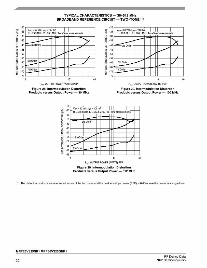
TYPICAL CHARACTERISTICS — 30--512 MHzBROADBAND REFERENCE CIRCUIT — TWO--TONE (1)
Figure 28. Intermodulation DistortionProducts versus Output Power — 30 MHz
--75
--20
10
7th Order
Pout, OUTPUT POWER (WATTS) PEP
--30
--40
--50
40
IMD,INTERMODULATIONDISTORTION(dBc)
--605th Order
1
--70
--25
--35
--45
--55
--65
VDD = 50 Vdc, IDQ = 100 mAf1 = 29.9 MHz, f2 = 30.1 MHz, Two--Tone Measurements
3rd Order
Figure 29. Intermodulation DistortionProducts versus Output Power — 100 MHz
--75
--20
10
7th Order
Pout, OUTPUT POWER (WATTS) PEP
--30
--40
--50
40
IMD,INTERMODULATIONDISTORTION(dBc)
--60
1
--70
--25
--35
--45
--55
--65
VDD = 50 Vdc, IDQ = 100 mAf1 = 99.9 MHz, f2 = 100.1 MHz, Two--Tone Measurements
3rd Order
5th Order
Figure 30. Intermodulation DistortionProducts versus Output Power — 512 MHz
--75
--20
10
7th Order
Pout, OUTPUT POWER (WATTS) PEP
--30
--40
--50
40
IMD,INTERMODULATIONDISTORTION(dBc)
--60
1
--70
--25
--35
--45
--55
--65
VDD = 50 Vdc, IDQ = 100 mAf1 = 511.9 MHz, f2 = 512.1 MHz, Two--Tone Measurements
3rd Order
5th Order
1. The distortion products are referenced to one of the two tones and the peak envelope power (PEP) is 6 dB above the power in a single tone.

MRFE6VS25NR1 MRFE6VS25GNR1
21RF Device DataNXP Semiconductors
30--512 MHz BROADBAND REFERENCE CIRCUIT
Zo = 50
Zsource
f = 30 MHz
Zload
f = 30 MHz
f = 512 MHz
f = 512 MHz
VDD = 50 Vdc, IDQ = 25 mA, Pout = 25 W CW
fMHz
Zsource
Zload
30 7.60 - j0.40 18.3 + j9.40
64 9.30 + j1.40 21.9 + j4.00
88 10.3 + j1.40 22.2 + j1.90
98 10.6 + j1.20 22.2 + j1.40
100 10.7 + j1.20 22.3 + j1.30
108 10.9 + j0.90 22.5 + j0.50
144 10.7 - j0.40 21.2 - j1.50
170 9.70 - j0.60 19.8 - j1.80
230 8.10 + j0.30 17.4 - j0.80
352 7.20 + j4.30 17.0 + j2.80
450 7.40 + j5.00 21.3 + j4.60
512 8.10 + j7.60 25.2 + j5.90
Zsource = Test circuit impedance as measured fromgate to ground.
Zload = Test circuit impedance as measured fromdrain to ground.
Figure 31. Broadband Series Equivalent Source and Load Impedance — 30--512 MHz
InputMatchingNetwork
DeviceUnderTest
OutputMatchingNetwork
Zsource Zload
5050

22RF Device Data
NXP Semiconductors
MRFE6VS25NR1 MRFE6VS25GNR1
1030 MHz NARROWBAND REFERENCE CIRCUIT
Table 17. 1030 MHz Narrowband Performance (In NXP Reference Circuit, 50 ohm system)VDD = 50 Volts, IDQ = 25 mA
Signal TypePout(W)
f(MHz)
Gps(dB)
D(%)
CW 25 1030 22.5 60.0
Table 18. Load Mismatch/Ruggedness (In NXP Reference Circuit)
Frequency(MHz) Signal Type VSWR
Pin(W) Test Voltage, VDD Result
1030 CW >65:1at all PhaseAngles
0.34(3 dB Overdrive)
50 No DeviceDegradation
MRFE6VS25NR1 MRFE6VS25GNR1
23RF Device DataNXP Semiconductors
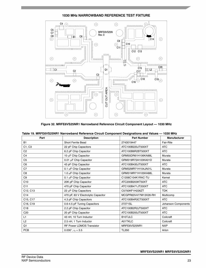
1030 MHz NARROWBAND REFERENCE TEST FIXTURE
Figure 32. MRFE6VS25NR1 Narrowband Reference Circuit Component Layout — 1030 MHz
MRFE6VS25NRev. 0
CUTOUTAREA
C4
C5C7C8 B1 C6
C1 C2 Q1
C3
C14
C12 C13
C9C10
C11
C15L1
C16
C17
C18
L2C20
C19
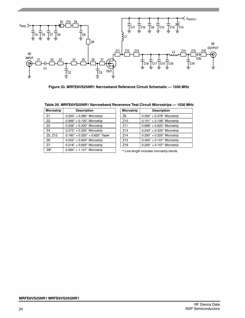
Table 19. MRFE6VS25NR1 Narrowband Reference Circuit Component Designations and Values — 1030 MHzPart Description Part Number Manufacturer
B1 Short Ferrite Bead 2743019447 Fair-Rite
C1, C3 22 pF Chip Capacitors ATC100B220JT500XT ATC
C2 6.2 pF Chip Capacitor ATC100B6R2BT500XT ATC
C4 10 F Chip Capacitor GRM55DR61H106KA88L Murata
C5 0.01 F Chip Capacitor GRM319R72A103KA01D Murata
C6 43 pF Chip Capacitor ATC100B430JT500XT ATC
C7 0.1 F Chip Capacitor GRM32MR71H104JA01L Murata
C8 1.0 F Chip Capacitor GRM31MR71H105KA88L Murata
C9 0.1 F Chip Capacitor C1206C104K1RAC-TU Kemet
C10 20K pF Chip Capacitor ATC200B203KT50XT ATC
C11 470 pF Chip Capacitor ATC100B471JT200XT ATC
C12, C13 22 F Chip Capacitors C5750KF1H226ZT TDK
C14 470 pF, 63 V Electrolytic Capacitor MCGPR63V477M13X26-RH Multicomp
C15, C17 4.3 pF Chip Capacitors ATC100B4R3CT500XT ATC
C16, C19 0.6-4.5 pF Tuning Capacitors 27271SL Johanson Components
C18 2.2 pF Chip Capacitor ATC100B2R2JT500XT ATC
C20 20 pF Chip Capacitor ATC100B200JT500XT ATC
L1 43 nH, 10 Turn Inductor B10TJLC Coilcraft
L2 2.5 nH, 1 Turn Inductor A01TKLC Coilcraft
Q1 RF Power LDMOS Transistor MRFE6VS25NR1 NXP
PCB 0.030, r = 3.5 TL350 Arlon
24RF Device Data
NXP Semiconductors
MRFE6VS25NR1 MRFE6VS25GNR1
Z1 0.200 0.080 Microstrip
Z2 0.569 0.120 Microstrip
Z3 0.339 0.320 Microstrip
Z4 0.272 0.320 Microstrip
Z5, Z12 0.160 0.320 0.620 Taper
Z6 0.522 0.620 Microstrip
Z7 0.218 0.620 Microstrip
Z8* 0.094 1.121 Microstrip
Z9 0.350 0.378 Microstrip
Z10 0.151 0.108 Microstrip
Z11 0.699 0.620 Microstrip
Z13 0.243 0.320 Microstrip
Z14 0.350 0.320 Microstrip
Z15 0.450 0.107 Microstrip
Z16 0.200 0.107 Microstrip
* Line length includes microstrip bends
Table 20. MRFE6VS25NR1 Narrowband Reverence Test Circuit Microstrips — 1030 MHz
DescriptionMicrostrip DescriptionMicrostrip
Figure 33. MRFE6VS25NR1 Narrowband Reference Circuit Schematic — 1030 MHz
Z1
RFINPUT
C1
Z2 Z4
DUT
C20
RFOUTPUT
VBIAS
VSUPPLY
C5
C11 C14
+
Z14
Z3 Z5
C7
Z13Z12Z11
Z8
Z7Z6
C4
Z15
C10
C2 C3
B1
C8L1
C19
Z16
Z9
C6
C9 C12 C13
L2
C18C15C17C16
Z10

MRFE6VS25NR1 MRFE6VS25GNR1
25RF Device DataNXP Semiconductors
TYPICAL CHARACTERISTICS — 1030 MHzNARROWBAND REFERENCE CIRCUIT
0
VGS, GATE--SOURCE VOLTAGE (VOLTS)
Figure 34. CW Output Power versus Gate--SourceVoltage at a Constant Input Power
0
30
P out,OUTPUTPOWER
(WATTS)
20
10
0.5 1 2.5 31.5 2 3.5
VDD = 50 VdcPin = 0.14 Wf = 1030 MHz
25
15
5
Figure 35. CW Output Power versus Input Power
Pin, INPUT POWER (dBm)
38
42
P out,OUTPUTPOWER
(dBm
)
40
44
46
3616 18
1030 29 31
f(MHz)
P1dB(W)
P3dB(W)
22 26
VDD = 50 VdcIDQ = 25 mAf = 1030 MHz
19
23
025
65
10
22
21
50
45
40
35
30
Pout, OUTPUT POWER (WATTS)
Figure 36. Power Gain and Drain Efficiencyversus CW Output Power
Gps,POWER
GAIN(dB)
D,DRAINEFFICIENCY(%)
21.5
20.5
20
30 35
22.5
55
Gps
VDD = 50 VdcIDQ = 25 mAf = 1030 MHz
D19.5
15 20 25
60
4 20 24
5
26RF Device Data
NXP Semiconductors
MRFE6VS25NR1 MRFE6VS25GNR1
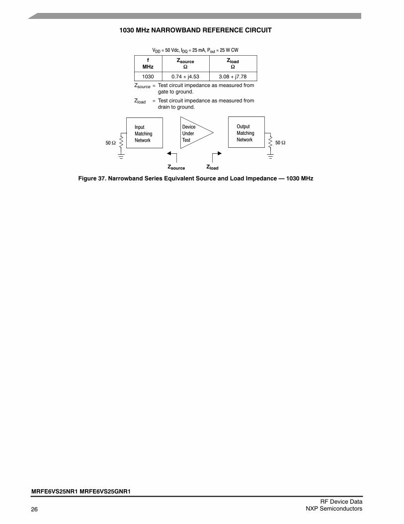
1030 MHz NARROWBAND REFERENCE CIRCUIT
VDD = 50 Vdc, IDQ = 25 mA, Pout = 25 W CW
fMHz
Zsource
Zload
1030 0.74 + j4.53 3.08 + j7.78
Zsource = Test circuit impedance as measured fromgate to ground.
Zload = Test circuit impedance as measured fromdrain to ground.
Figure 37. Narrowband Series Equivalent Source and Load Impedance — 1030 MHz
InputMatchingNetwork
DeviceUnderTest
OutputMatchingNetwork
Zsource Zload
5050

MRFE6VS25NR1 MRFE6VS25GNR1
27RF Device DataNXP Semiconductors
PACKAGE DIMENSIONS
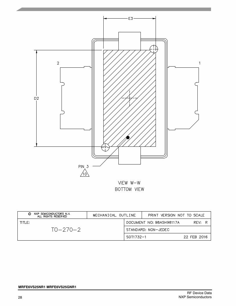
28RF Device Data
NXP Semiconductors
MRFE6VS25NR1 MRFE6VS25GNR1

MRFE6VS25NR1 MRFE6VS25GNR1
29RF Device DataNXP Semiconductors

30RF Device Data
NXP Semiconductors
MRFE6VS25NR1 MRFE6VS25GNR1
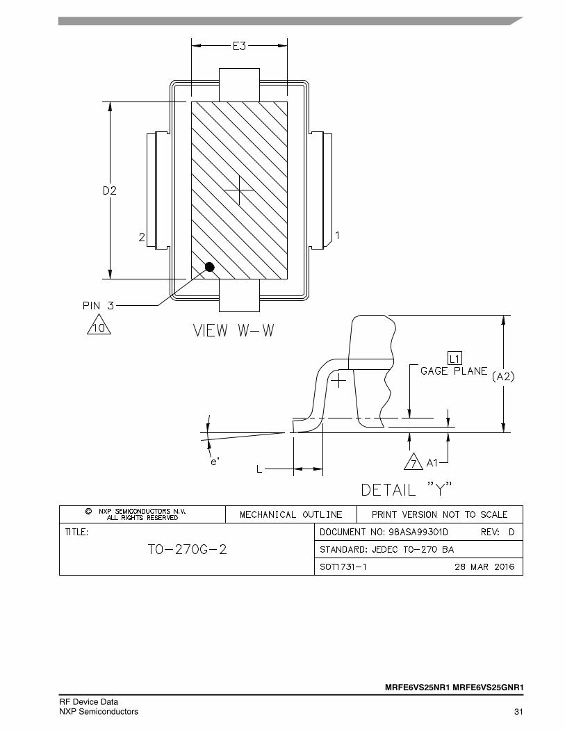
MRFE6VS25NR1 MRFE6VS25GNR1
31RF Device DataNXP Semiconductors

32RF Device Data
NXP Semiconductors
MRFE6VS25NR1 MRFE6VS25GNR1
MRFE6VS25NR1 MRFE6VS25GNR1
33RF Device DataNXP Semiconductors
PRODUCT DOCUMENTATION, SOFTWARE AND TOOLS
Refer to the following documents, software and tools to aid your design process.
Application Notes AN1907: Solder Reflow Attach Method for High Power RF Devices in Over--Molded Plastic Packages
AN1955: Thermal Measurement Methodology of RF Power Amplifiers
AN3263: Bolt Down Mounting Method for High Power RF Transistors and RFICs in Over--Molded Plastic Packages
AN3789: Clamping of High Power RF Transistors and RFICs in Over--Molded Plastic Packages
Engineering Bulletins EB212: Using Data Sheet Impedances for RF LDMOS Devices
EB38: Measuring the Intermodulation Distortion of Linear Amplifiers
Software Electromigration MTTF Calculator
RF High Power Model
.s2p File
Development Tools Printed Circuit Boards
For Software and Tools, do a Part Number search at http://www.nxp.com, and select the “Part Number” link. Go to theSoftware & Tools tab on the part’s Product Summary page to download the respective tool.
REVISION HISTORY
The following table summarizes revisions to this document.
Revision Date Description
0 June 2012 Initial Release of Data Sheet
1 Dec. 2012 Added part number MRFE6VS25GNR1, p. 1 Added 1265A--03 (TO--270--2 Gull) package isometric, p. 1, and Mechanical Outline, p. 30--32 Load Mismatch/Ruggedness tables: changed output power to input power to clarify the conditions used
during test, p. 1, 3, 9, 22
Figs. 17, 18 and 19, Intermodulation Distortion Products versus Output Power (1.8, 10, 30 MHz): correctedx--axis data to show Watts (PEP) measurement, p. 13
Added 30--512 MHz Broadband Reference Circuit as follows:-- Typical Performance table, p. 1-- Table 12, Broadband Performance, p. 15-- Table 13, Load Mismatch/Ruggedness, p. 15-- Fig. 21, Broadband Reference Circuit Component Layout, p. 16-- Table 14, Broadband Reference Circuit Component Designations and Values, p. 16-- Fig. 21a, Detailed View of Semi--flex Cables with Shields and #61 Multi--aperture Cores, p. 17-- Fig. 22, Broadband Reference Circuit Schematic, p. 17-- Table 15, Broadband Reference Circuit Microstrips, p. 17-- Fig. 23, Power Gain, CW Output Power and Drain Efficiency versus Frequency at a Constant InputPower, p. 18
-- Fig. 24, CW Output Power versus Gate--Source Voltage at a Constant Input Power, Pin = 0.65 W, p. 18-- Fig. 25, CW Output Power versus Gate--Source Voltage at a Constant Input Power, Pin = 0.325 W, p. 18-- Fig. 26, CW Output Power versus Input Power, p. 19-- Fig. 27, Power Gain and Drain Efficiency versus CW Output Power, p. 19-- Fig. 28, Intermodulation Distortion Products versus Output Power -- 30 MHz, p. 20-- Fig. 29, Intermodulation Distortion Products versus Output Power -- 100 MHz, p. 20-- Fig. 30, Intermodulation Distortion Products versus Output Power -- 512 MHz, p. 20-- Fig. 31, Broadband Series Equivalent Source and Load Impedance, p. 21
2 Mar. 2019 Fig. 1, Pin Connections, corrected Drain (Pin 1) and Gate (Pin 2) to reflect correct pin numbers, p. 1
Table 6, Ordering Information, added table, p. 3
Package Outline Drawings: TO--270--2 package outline updated to Rev. R, pp. 27–29. TO--270G--2package outline updated to Rev. D, pp. 30–32.
34RF Device Data
NXP Semiconductors
MRFE6VS25NR1 MRFE6VS25GNR1
How to Reach Us:
Home Page:nxp.com
Web Support:nxp.com/support
Information in this document is provided solely to enable system and softwareimplementers to use NXP products. There are no express or implied copyright licensesgranted hereunder to design or fabricate any integrated circuits based on the informationin this document. NXP reserves the right to make changes without further notice to anyproducts herein.
NXP makes no warranty, representation, or guarantee regarding the suitability of itsproducts for any particular purpose, nor does NXP assume any liability arising out of theapplication or use of any product or circuit, and specifically disclaims any and all liability,including without limitation consequential or incidental damages. “Typical” parametersthat may be provided in NXP data sheets and/or specifications can and do vary indifferent applications, and actual performance may vary over time. All operatingparameters, including “typicals,” must be validated for each customer application bycustomer’s technical experts. NXP does not convey any license under its patent rightsnor the rights of others. NXP sells products pursuant to standard terms and conditions ofsale, which can be found at the following address: nxp.com/SalesTermsandConditions.
NXP, the NXP logo, Freescale and the Freescale logo are trademarks of NXP B.V.All other product or service names are the property of their respective owners.E 2012, 2019 NXP B.V.
Document Number: MRFE6VS25NRev. 2, 03/2019
Related Documents