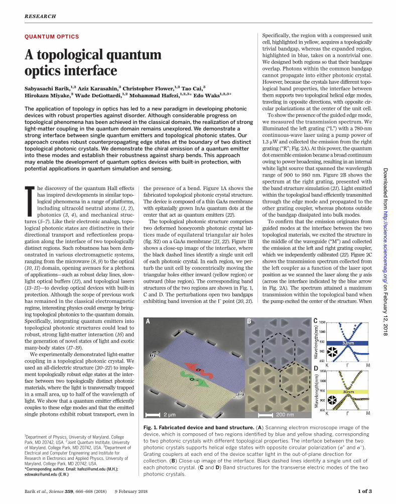
QUANTUM OPTICS A topological quantum optics interface Sabyasachi Barik, 1,2 Aziz Karasahin, 3 Christopher Flower, 1,2 Tao Cai, 3 Hirokazu Miyake, 2 Wade DeGottardi, 1,2 Mohammad Hafezi, 1,2,3 * Edo Waks 1,2,3 * The application of topology in optics has led to a new paradigm in developing photonic devices with robust properties against disorder. Although considerable progress on topological phenomena has been achieved in the classical domain, the realization of strong light-matter coupling in the quantum domain remains unexplored. We demonstrate a strong interface between single quantum emitters and topological photonic states. Our approach creates robust counterpropagating edge states at the boundary of two distinct topological photonic crystals. We demonstrate the chiral emission of a quantum emitter into these modes and establish their robustness against sharp bends. This approach may enable the development of quantum optics devices with built-in protection, with potential applications in quantum simulation and sensing. T he discovery of the quantum Hall effects has inspired developments in similar topo- logical phenomena in a range of platforms, including ultracold neutral atoms (1, 2), photonics (3, 4), and mechanical struc- tures (5–7). Like their electronic analogs, topo- logical photonic states are distinctive in their directional transport and reflectionless propa- gation along the interface of two topologically distinct regions. Such robustness has been dem- onstrated in various electromagnetic systems, ranging from the microwave (8, 9) to the optical (10, 11) domain, opening avenues for a plethora of applications—such as robust delay lines, slow- light optical buffers (12), and topological lasers (13–15)—to develop optical devices with built-in protection. Although the scope of previous work has remained in the classical electromagnetic regime, interesting physics could emerge by bring- ing topological photonics to the quantum domain. Specifically, integrating quantum emitters into topological photonic structures could lead to robust, strong light-matter interaction (16) and the generation of novel states of light and exotic many-body states (17–19). We experimentally demonstrated light-matter coupling in a topological photonic crystal. We used an all-dielectric structure (20–22) to imple- ment topologically robust edge states at the inter- face between two topologically distinct photonic materials, where the light is transversally trapped in a small area, up to half of the wavelength of light. We show that a quantum emitter efficiently couples to these edge modes and that the emitted single photons exhibit robust transport, even in the presence of a bend. Figure 1A shows the fabricated topological photonic crystal structure. The device is composed of a thin GaAs membrane with epitaxially grown InAs quantum dots at the center that act as quantum emitters (22). The topological photonic structure comprises two deformed honeycomb photonic crystal lat- tices made of equilateral triangular air holes (fig. S2) on a GaAs membrane (21, 22). Figure 1B shows a close-up image of the interface, where the black dashed lines identify a single unit cell of each photonic crystal. In each region, we per- turb the unit cell by concentrically moving the triangular holes either inward (yellow region) or outward (blue region). The corresponding band structures of the two regions are shown in Fig. 1, C and D. The perturbations open two bandgaps exhibiting band inversion at the G point (20, 21). Specifically, the region with a compressed unit cell, highlighted in yellow, acquires a topologically trivial bandgap, whereas the expanded region, highlighted in blue, takes on a nontrivial one. We designed both regions so that their bandgaps overlap. Photons within the common bandgap cannot propagate into either photonic crystal. However, because the crystals have different topo- logical band properties, the interface between them supports two topological helical edge modes, traveling in opposite directions, with opposite cir- cular polarizations at the center of the unit cell. To show the presence of the guided edge mode, we measured the transmission spectrum. We illuminated the left grating (“L”) with a 780-nm continuous-wave laser using a pump power of 1.3 mW and collected the emission from the right grating (“R”; Fig. 2A). At this power, the quantum dot ensemble emission became a broad continuum owing to power broadening, resulting in an internal white light source that spanned the wavelength range of 900 to 980 nm. Figure 2B shows the spectrum at the right grating, presented with the band structure simulation (21). Light emitted within the topological band efficiently transmitted through the edge mode and propagated to the other grating coupler, whereas photons outside of the bandgap dissipated into bulk modes. To confirm that the emission originates from guided modes at the interface between the two topological materials, we excited the structure in the middle of the waveguide (“M”) and collected the emission at the left and right grating coupler, which we independently calibrated ( 22). Figure 2C shows the transmission spectrum collected from the left coupler as a function of the laser spot position as we scanned the laser along the y axis (across the interface indicated by the blue arrow in Fig. 2A). The spectrum attained a maximum transmission within the topological band when the pump excited the center of the structure. When RESEARCH Barik et al., Science 359, 666–668 (2018) 9 February 2018 1 of 3 1 Department of Physics, University of Maryland, College Park, MD 20742, USA. 2 Joint Quantum Institute, University of Maryland, College Park, MD 20742, USA. 3 Department of Electrical and Computer Engineering and Institute for Research in Electronics and Applied Physics, University of Maryland, College Park, MD 20742, USA. *Corresponding author. Email: [email protected] (M.H.); [email protected] (E.W.) Fig. 1. Fabricated device and band structure. (A) Scanning electron microscope image of the device, which is composed of two regions identified by blue and yellow shading, corresponding to two photonic crystals with different topological properties. The interface between the two photonic crystals supports helical edge states with opposite circular polarization (s + and s – ). Grating couplers at each end of the device scatter light in the out-of-plane direction for collection. (B) Close-up image of the interface. Black dashed lines identify a single unit cell of each photonic crystal. (C and D) Band structures for the transverse electric modes of the two photonic crystals. on February 12, 2018 http://science.sciencemag.org/ Downloaded from

Welcome message from author
This document is posted to help you gain knowledge. Please leave a comment to let me know what you think about it! Share it to your friends and learn new things together.
Transcript
QUANTUM OPTICS
A topological quantumoptics interfaceSabyasachi Barik,1,2 Aziz Karasahin,3 Christopher Flower,1,2 Tao Cai,3
Hirokazu Miyake,2 Wade DeGottardi,1,2 Mohammad Hafezi,1,2,3* Edo Waks1,2,3*
The application of topology in optics has led to a new paradigm in developing photonicdevices with robust properties against disorder. Although considerable progress ontopological phenomena has been achieved in the classical domain, the realization of stronglight-matter coupling in the quantum domain remains unexplored. We demonstrate astrong interface between single quantum emitters and topological photonic states. Ourapproach creates robust counterpropagating edge states at the boundary of two distincttopological photonic crystals. We demonstrate the chiral emission of a quantum emitterinto these modes and establish their robustness against sharp bends. This approachmay enable the development of quantum optics devices with built-in protection, withpotential applications in quantum simulation and sensing.
The discovery of the quantum Hall effectshas inspired developments in similar topo-logical phenomena in a range of platforms,including ultracold neutral atoms (1, 2),photonics (3, 4), and mechanical struc-
tures (5–7). Like their electronic analogs, topo-logical photonic states are distinctive in theirdirectional transport and reflectionless propa-gation along the interface of two topologicallydistinct regions. Such robustness has been dem-onstrated in various electromagnetic systems,ranging from the microwave (8, 9) to the optical(10, 11) domain, opening avenues for a plethoraof applications—such as robust delay lines, slow-light optical buffers (12), and topological lasers(13–15)—to develop optical devices with built-inprotection. Although the scope of previous workhas remained in the classical electromagneticregime, interesting physics could emerge by bring-ing topological photonics to the quantum domain.Specifically, integrating quantum emitters intotopological photonic structures could lead torobust, strong light-matter interaction (16) andthe generation of novel states of light and exoticmany-body states (17–19).We experimentally demonstrated light-matter
coupling in a topological photonic crystal. Weused an all-dielectric structure (20–22) to imple-ment topologically robust edge states at the inter-face between two topologically distinct photonicmaterials, where the light is transversally trappedin a small area, up to half of the wavelength oflight. We show that a quantum emitter efficientlycouples to these edge modes and that the emittedsingle photons exhibit robust transport, even in
the presence of a bend. Figure 1A shows thefabricated topological photonic crystal structure.The device is composed of a thin GaAs membranewith epitaxially grown InAs quantum dots at thecenter that act as quantum emitters (22).The topological photonic structure comprises
two deformed honeycomb photonic crystal lat-tices made of equilateral triangular air holes(fig. S2) on a GaAs membrane (21, 22). Figure 1Bshows a close-up image of the interface, wherethe black dashed lines identify a single unit cellof each photonic crystal. In each region, we per-turb the unit cell by concentrically moving thetriangular holes either inward (yellow region) oroutward (blue region). The corresponding bandstructures of the two regions are shown in Fig. 1,C and D. The perturbations open two bandgapsexhibiting band inversion at the G point (20, 21).
Specifically, the region with a compressed unitcell, highlighted in yellow, acquires a topologicallytrivial bandgap, whereas the expanded region,highlighted in blue, takes on a nontrivial one.We designed both regions so that their bandgapsoverlap. Photons within the common bandgapcannot propagate into either photonic crystal.However, because the crystals have different topo-logical band properties, the interface betweenthem supports two topological helical edge modes,traveling in opposite directions, with opposite cir-cular polarizations at the center of the unit cell.To show the presence of the guided edgemode,
we measured the transmission spectrum. Weilluminated the left grating (“L”) with a 780-nmcontinuous-wave laser using a pump power of1.3 mW and collected the emission from the rightgrating (“R”; Fig. 2A). At this power, the quantumdot ensemble emissionbecameabroad continuumowing to power broadening, resulting in an internalwhite light source that spanned the wavelengthrange of 900 to 980 nm. Figure 2B shows thespectrum at the right grating, presented withthe band structure simulation (21). Light emittedwithin the topological band efficiently transmittedthrough the edge mode and propagated to theother grating coupler, whereas photons outsideof the bandgap dissipated into bulk modes.To confirm that the emission originates from
guided modes at the interface between the twotopological materials, we excited the structure inthe middle of the waveguide (“M”) and collectedthe emission at the left and right grating coupler,which we independently calibrated (22). Figure 2Cshows the transmission spectrum collected fromthe left coupler as a function of the laser spotposition as we scanned the laser along the y axis(across the interface indicated by the blue arrowin Fig. 2A). The spectrum attained a maximumtransmission within the topological band whenthe pump excited the center of the structure. When
RESEARCH
Barik et al., Science 359, 666–668 (2018) 9 February 2018 1 of 3
1Department of Physics, University of Maryland, CollegePark, MD 20742, USA. 2Joint Quantum Institute, Universityof Maryland, College Park, MD 20742, USA. 3Department ofElectrical and Computer Engineering and Institute forResearch in Electronics and Applied Physics, University ofMaryland, College Park, MD 20742, USA.*Corresponding author. Email: [email protected] (M.H.);[email protected] (E.W.)
Fig. 1. Fabricated device and band structure. (A) Scanning electron microscope image of thedevice, which is composed of two regions identified by blue and yellow shading, correspondingto two photonic crystals with different topological properties. The interface between the twophotonic crystals supports helical edge states with opposite circular polarization (s+ and s–).Grating couplers at each end of the device scatter light in the out-of-plane direction forcollection. (B) Close-up image of the interface. Black dashed lines identify a single unit cell ofeach photonic crystal. (C and D) Band structures for the transverse electric modes of the twophotonic crystals.
on February 12, 2018
http://science.sciencemag.org/
Dow
nloaded from

we displaced the excitation beam by ~1.5 mm alongthe y direction, the transmission vanished, in-dicating that the photons were coming only fromthe waveguide.A key feature of topological edge modes is
the chiral nature of the coupling between thehelical topological edge mode and the quantumemitter. Specifically, different dipole spins radi-atively couple to opposite propagating helicaledge states. To demonstrate this helical light-matter coupling, we applied a magnetic field inthe out-of-plane (Faraday) direction on the entiresample. This field induced a Zeeman splitting inthe quantum dot excited state, resulting in twonondegenerate states that emitted with oppositecircular polarizations (fig. S5), denoted as s±
(Fig. 3A) (22, 23). Although this magnetic fielddoes not play a role in the topological natureof the waveguide, it enabled us to identify thepolarization of the dipole by the frequency ofemitted photons. By spectrally resolving the emis-sions, we were able to identify the dipole spinand correlate it with the propagation directionof the emitted photon.To isolate a single quantum emitter within the
topological edge mode, we reduced the power to10 nW, which is well below the quantum dot sat-uration power. Using the intensities of the col-lected light at the two ends, we calculated a lowerbound on the coupling efficiency of 68% (tableS1), defined as the ratio of the photon emissionrate into the waveguide to the total emission rate(22). This high efficiency is due to the tight elec-tromagnetic confinement of the guided modes,which enhances light-matter interactions. Figure3B shows the emission spectrum as a function ofmagnetic field, where we collected the emissiondirectly from point M indicated in Fig. 2A. Asthe magnetic field increases, the quantum dotresonance splits into two branches correspond-ing to the two Zeeman split bright exciton states.We compared this spectrum with the one col-lected from the left and right gratings (Fig. 3, Cand D). At the left grating, we observed onlythe emission from the s– branch, whereas atthe right grating, we observed only the emissionfrom the s+ branch. These results establish thechiral emission and spin-momentum lockingof the emitted photons and provide strong evi-dence that the emitter is coupling to topologicaledge states that exhibit unidirectional transport.Such chiral coupling is in direct analogy to one-dimensional systems (16, 24, 25); however, thewaveguided modes of our structure originatefrom two-dimensional topology. As a result, thetopological edge mode should exhibit robustnessto certain deformations, such as bends.To establish this topological robustness, we
analyzed the propagation of emitted photons inthe presence of a bend. We introduced a 60° bendinto the structure, as shown in Fig. 4A, and per-formed measurements similar to those in Fig. 3.Again, we observed that emitted photons prop-agate in opposite directions in a chiral fashionand arrive at the grating associated with theirrespective polarization (Fig. 4, B and C). Thepreservation of the chiral nature of the emission
Barik et al., Science 359, 666–668 (2018) 9 February 2018 2 of 3
Fig. 2. Transmission characteristics of the topological waveguide. (A) A schematic of theexcitation scheme identifying the three relevant regions (L, left grating; R, right grating; M, middleof the waveguide). (B) Simulated band structure of transverse electromagnetic modes of astraight topological waveguide. The gray region corresponds to bulk modes of the individualtopological photonic crystals, and red lines represent modes within the bandgap corresponding totopological edge states. The adjacent panel shows the measured spectrum at the transmitted endof the waveguide. The red shaded region identifies the topological edge band. kx, reciprocal wavevector; a, lattice constant. (C) Transmission spectrum at point L as a function of the excitationlaser position.
Fig. 3. Chirality in a straight topological waveguide. (A) Schematic of quantum dot–levelstructure in the presence of a magnetic field and radiative transitions with opposite circularpolarizations. (B) Emission spectrum collected from the excitation region as a functionof magnetic field (B). (C and D) Transmission spectra to left and right gratings, respectively.
RESEARCH | REPORTon February 12, 2018
http://science.sciencemag.org/
Dow
nloaded from

demonstrates an absence of back-reflection atthe bend, which would result in a strong signalfor both polarizations at the left grating. Wealso confirmed that these routed photons aresingle photons by performing a second-ordercorrelation measurement for photons collectedfrom both ends of the waveguide, which exhibitsstrong antibunching (Fig. 4, D and E). The ro-bustness in this system is due to C6v symmetry,and the boundary and disorder can break thissymmetry and lead to backscattering of the edgemodes. In the supplementary materials, we anal-yze the effect of certain types of disorder on thetransmission properties of the edge modes andshow that the unidirectional propagation is robust.The full characterization of robustness, beyondnumerical simulations and the tight-bindingmodel(26), requires further study.
In this work, we demonstrated coupling be-tween single quantum emitters and topologicallyrobust photonic edge states. Our approach opensnew prospects at the interface of quantum opticsand topological photonics. In the context of chiralquantum optics, one can explore new regimes ofdipole emission in the vicinity of topologicalphotonic structures and exploit the robustnessof the electromagnetic modes (16). Furthermore,in a chiral waveguide, photon-mediated interac-tions between emitters are location-independent(27). This property could facilitate the couplingof multiple solid-state emitters via photons whileovercoming scalability issues associated with ran-dom emitter position, enabling large-scale super-radiant states and spin-squeezing. Ultimately,such an approach could constitute a versatileplatform to explore many-body quantum physics
at a topological edge (28), create chiral spinnetworks (27, 29), and realize fractional quan-tum Hall states of light (30, 31).
REFERENCES AND NOTES
1. J. Dalibard, F. Gerbier, G. Juzeliūnas, P. Öhberg, Rev. Mod. Phys.83, 1523–1543 (2011).
2. C. Eckardt, Rev. Mod. Phys. 89, 011004 (2017).3. M. Hafezi, J. M. Taylor, Phys. Today 67, 68–69 (2014).4. L. Lu, J. D. Joannopoulos, M. Soljačić, Nat. Photonics 8,
821–829 (2014).5. L. Kane, T. C. Lubensky, Nat. Phys. 10, 39–45 (2014).6. J. Paulose, B. G. G. Chen, V. Vitelli, Nat. Phys. 11, 153–156
(2015).7. R. Süsstrunk, S. D. Huber, Science 349, 47–50 (2015).8. Z. Wang, Y. Chong, J. D. Joannopoulos, M. Soljacić, Nature 461,
772–775 (2009).9. X. Cheng et al., Nat. Mater. 15, 542–548 (2016).10. M. Hafezi, S. Mittal, J. Fan, A. Migdall, J. M. Taylor,
Nat. Photonics 7, 1001–1005 (2013).11. M. C. Rechtsman et al., Nature 496, 196–200 (2013).12. M. Hafezi, E. A. Demler, M. D. Lukin, J. M. Taylor, Nat. Phys. 7,
907–912 (2011).13. L. Pilozzi, C. Conti, Phys. Rev. B 93, 195317 (2016).14. G. Harari et al., “Topological lasers,” in Conference on Lasers and
Electro-Optics [OSA Technical Digest (online), Optical Society ofAmerica, 2016], FM3A.3.
15. P. St-Jean et al., Nat. Photonics 11, 651–656 (2017).16. P. Lodahl et al., Nature 541, 473–480 (2017).17. I. Carusotto, C. Ciuti, Rev. Mod. Phys. 85, 299–366
(2013).18. J. I. Cirac, H. J. Kimble, Nat. Photonics 11, 18–20 (2017).19. D. G. Angelakis, Ed., Quantum Simulations with Photons and
Polaritons (Springer International Publishing, 2017).20. L. H. Wu, X. Hu, Phys. Rev. Lett. 114, 223901 (2015).21. S. Barik, H. Miyake, W. DeGottardi, E. Waks, M. Hafezi,
New J. Phys. 18, 113013 (2016).22. Materials and methods are available as supplementary materials.23. M. Bayer et al., Phys. Rev. B 65, 195315 (2002).24. J. Petersen, J. Volz, A. Rauschenbeutel, Science 346, 67–71
(2014).25. I. Söllner et al., Nat. Nanotechnol. 10, 775–778 (2015).26. T. Kariyado, X. Hu, Sci. Rep. 7, 16515 (2017).27. H. Pichler, T. Ramos, A. J. Daley, P. Zoller, Phys. Rev. A 91,
042116 (2014).28. M. Ringel, M. Pletyukhov, V. Gritsev, New J. Phys. 16, 113030
(2014).29. A. Metelmann, A. A. Clerk, Phys. Rev. X 5, 021025 (2015).30. R. O. Umucalılar, I. Carusotto, Phys. Rev. Lett. 108, 206809 (2012).31. M. Hafezi, M. D. Lukin, J. M. Taylor, New J. Phys. 15, 063001
(2013).
ACKNOWLEDGMENTS
The authors acknowledge fruitful discussions with S. Mittal.All data needed to evaluate the conclusions are present in thepaper and/or the supplementary materials. This research wassupported by the Office of Naval Research, the Air ForceOffice of Scientific Research–Multidisciplinary UniversityResearch Initiative (grant FA9550-16-1-0323), the SloanFoundation, and the Physics Frontier Center at the JointQuantum Institute.
SUPPLEMENTARY MATERIALS
www.sciencemag.org/content/359/6376/666/suppl/DC1Materials and MethodsSupplementary TextFigs. S1 to S5Table S1
24 September 2017; accepted 11 December 201710.1126/science.aaq0327
Barik et al., Science 359, 666–668 (2018) 9 February 2018 3 of 3
Fig. 4. Robust transport in two dimensions along a bend. (A) Schematic of a modified topologicalwaveguide with a bend. (B and C) Photoluminescence collected from points L and R, respectively,showing only one branch of the quantum dot. (D and E) Second-order correlation measurement[g2(t), where t is the time delay] data obtained from points L and R, respectively, showing antibunching.Red dots represent the experimental data, and the black line corresponds to fitting.
RESEARCH | REPORTon February 12, 2018
http://science.sciencemag.org/
Dow
nloaded from

Materials and Methods Device Fabrication
To fabricate the device, we began with an initial wafer composed of a 160 nm GaAs membrane on top of 1 𝜇m sacrificial layer of Al0.8Ga0.2As with quantum dots grown at the center. The quantum dot density was approximately 50 𝜇m-2. Based on the given quantum density and cross-sectional area of the waveguide, the probability of finding two dots in the structure with the same resonance is less than 0.7%. Thus, it is extremely unlikely in a given device for a photon emitted by one dot to be scattered by a second.
We fabricated the topological photonic crystal structure using electron beam
lithography, followed by dry etching and selective wet etching of the sacrificial layer. We first spin-coated the wafer with ZEP520A e-beam resist, then patterned the structure using 100 keV acceleration voltage and developed the resist using ZED50 developer. After patterning, we used chlorine-based inductively coupled plasma etching to transfer the pattern on the GaAs membrane. We finally performed selective wet etching using HF to create a suspended structure with air on top and bottom. The rectangular structures in the periphery are included to facilitate undercut of the sacrificial layer.
Sharp corners with straight side walls are essential to observe the topological
helical edge modes. It is confirmed via simulation that triangles with rounded corners are detrimental for the device operation. However, even with highly directional dry etch, creating sharp features like triangles is challenging at such small length scales. We observed – by using a regular mask design (as shown in Figure S1.A) – that etching causes widening of holes which eventually results in rounded corners much like a Reuleaux triangle (Figure S1.B). We used a modified mask design to overcome this challenge. Triangles with shrunk edges shown in Figure S1.C are used as a mask; this results in sharp triangles with edge lengths of 140 nm. Close up SEM image of final structure is shown in Figure S1.D.
5
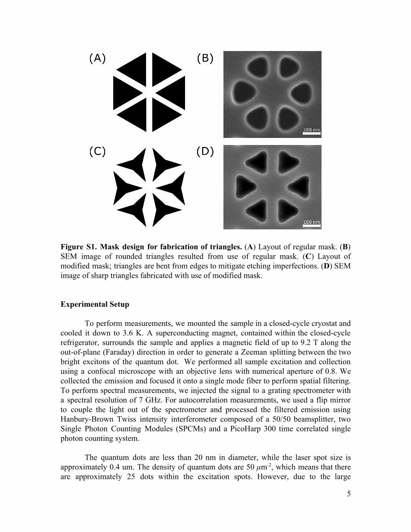
Figure S1. Mask design for fabrication of triangles. ( A ) Layout of regular mask. ( B) SEM image of rounded triangles resulted from use of regular mask. ( C ) Layout of modified mask; triangles are bent from edges to mitigate etching imperfections. ( D ) SEM image of sharp triangles fabricated with use of modified mask. Experimental Setup
To perform measurements, we mounted the sample in a closed-cycle cryostat and cooled it down to 3.6 K. A superconducting magnet, contained within the closed-cycle refrigerator, surrounds the sample and applies a magnetic field of up to 9.2 T along the out-of-plane (Faraday) direction in order to generate a Zeeman splitting between the two bright excitons of the quantum dot. We performed all sample excitation and collection using a confocal microscope with an objective lens with numerical aperture of 0.8. We collected the emission and focused it onto a single mode fiber to perform spatial filtering. To perform spectral measurements, we injected the signal to a grating spectrometer with a spectral resolution of 7 GHz. For autocorrelation measurements, we used a flip mirror to couple the light out of the spectrometer and processed the filtered emission using Hanbury-Brown Twiss intensity interferometer composed of a 50/50 beamsplitter, two Single Photon Counting Modules (SPCMs) and a PicoHarp 300 time correlated single photon counting system.
The quantum dots are less than 20 nm in diameter, while the laser spot size is
approximately 0.4 um. The density of quantum dots are 50 𝜇m-2, which means that there are approximately 25 dots within the excitation spots. However, due to the large
5

inhomogeneous broadening of the ensemble, each of these dots emits at a different wavelength. We isolate individual quantum dots by spectral filtering using a grating spectrometer with a resolution of 0.02 nm. The spectrometer selects the emission from only a single dot, as evidenced by the anti-bunching dip observed in Fig. 4D-E which dips below 0.5.
Supplementary Text
Device Design
Figure S2 shows a schematic of the device design. We begin with a honeycomb lattice of equilateral triangles exhibiting hexagonal symmetry as our baseline structure. This lattice is a triangular lattice of cells consisting of six equilateral triangular holes, indicated by the dashed line. We use a lattice constant of a0 = 445 nm, an edge length of the equilateral triangle of s =140 nm, and a slab thickness of h = 160 nm. R defines the distance from the center of a cell to the centroid of a triangle. In this structure a perfect honeycomb lattice corresponds to R = a0/3.
With these parameters we obtain doubly degenerate Dirac cones at 319 THz (940
nm). We form the two mirrors by concentrically expanding or contracting the unit cell. We create topologically distinct regions by deforming the unit cell of the pristine
honeycomb lattice. In the blue region in Figure 1A, we concentrically shift the triangular holes by increasing R to 1.05a0/3, thereby shifting all the triangular holes in an individual cell outward. This deformation results in the band structure shown in Figure 1C. In the yellow region, we decrease R to 0.94a0/3, which pulls the holes towards the center resulting in the band structure shown in Figure 1D.
Figure S2. Design of honeycomb-like photonic crystal.
5

Symmetry-Protected Topological Photonic Crystal
Once thought to be limited to the quantum Hall effect, the notion of topological insulating phases has revolutionized condensed matter physics and is the inspiration for topological photonic systems. These states are based on the fact that insulating Hamiltonians which obey certain combinations of symmetries (such as time-reversal) can be classified according to their topology. The photonic crystal considered here is described by a Z2 topological invariant, which takes the value 0 (trivial phase) or 1 (topological phase). The physical manifestation of this is that between regions of differing topology, protected edge modes are found. These modes cannot be coupled since such a term would violate the protected symmetry.
The photonic crystal considered in this work is an analog of a quantum spin Hall
system for photons and is discussed in greater detail in (20, 21) . The quantum spin Hall system exhibits topological protection that is based on time-reversal symmetry. In the context of the photonic crystal, the role of time-reversal symmetry is played by the six-fold rotational (C6v) crystal symmetry of the hexagonal unit cell. In the energy range of interest, the band structure of the system is described by the Dirac equation, where the mass is controlled by the spacing of triangles in a hexagonal cluster. The topological Z2 index reflects the sign of the mass, and is positive (negative) for compressed (expanded) regions. The topologically protected counterpropagating modes exist in the region at which the mass changes sign. In the context of the Dirac equation, these states are known as Jackiw-Rebbi states (21) .
The yellow and blue regions in Figure 1A represent the topologically distinct
phases discussed above. Topological modes exist at the boundary, and are protected from any disorder which respects the six-fold crystal symmetry. Disorder that breaks this symmetry can lead to the backscattering of the edge modes. In fact, the formation of the interface itself can break this symmetry, albeit weakly. Through extensive simulations, we have found that the zig-zag interface in our device adequately preserves the crystalline symmetry, thereby minimizing the coupling between the counterpropagating edge modes. Figure S3.A shows the propagating mode for this interface, while Figure S3.B shows the propagation length of the waveguide as a function of wavelength. The simulated propagation length is approximately 22 𝜇m. We note that although this propagation length is longer than our device (15 𝜇m), it is short compared to a conventional photonic crystal waveguide. This reduced propagation length is due to the fact that we are forming a guided mode from a perturbed hexagonal lattice. In the pure hexagonal lattice all modes exist below the light line (21), but after perturbation the structure exhibits a triangular rather than hexagonal symmetry. This change in symmetry can cause modes to scatter to the 𝚪 point which is above the light line. Using a progressively weaker perturbation leads to less scattering, and therefore longer propagation lengths (Figure S3.C), which must be traded off with a narrower topological bandgap. In Figure S3.D, we show simulations illustrating the robustness of the edge modes to a certain type of defect. The defect, an entire missing cell, breaks C6v crystal
5

symmetry. However, this defect does not adversely affect the transmission in the gapped region. We should note that the disorder seen in our device is considerably less severe.
Figure S3. Propagation loss and robustness of edge modes. (A) Simulation showing electric field intensity for propagation of edge state in a topological waveguide without a defect (B) Propagation length for the edge state in our measured device. The perturbation parameter is ΔR = R0 - Rin/out , where R is defined as in Fig S2. The parameter R0 corresponds to the unperturbed original honeycomb lattice, and Rin/out characterize the inward/outward perturbed lattices, respectively. (C) Simulation results showing propagation lengths of edge states in the topological photonic crystal waveguide as we change ΔR. (D) Simulation showing electric field intensity of edge states as it propagates around a defect. Grating Calibration
Since both left and right grating couplers are fabricated under similar condition they are identical in terms of coupling efficiency. To test this fact we calibrated them with respect to. the transmission spectrum of the topological waveguide. Figure S4.A shows the different positions on the device. We shine an intense excitation beam of 780 nm with 1.5uW power at the center of the waveguide (M). At this high power all the quantum dots are saturated and emit a broadband spectrum ranging from 900-980nm. We collected the transmitted signal from left (L) and right grating (R). Figure S4.B shows almost equal counts coming from both the gratings with almost overlapping transmission spectrum. Additionally, the area under the curves give approximately 40 million counts/sec for the gratings thus indicating equal coupling efficiency.
5

Figure S4. Transmission data from left and right gratings. ( A ) Scheme for excitation and collection. ( B) Transmitted signal collected from two gratings. Polarization of Quantum Dots in Bulk Under Magnetic Field
We first measured the photoluminescence from a bare QD in the bulk. With the application of magnetic field QD emission spectrum splitted into two branches with circularly polarized emission as shown in Figure S5. A and denoted by 𝜎 ±. At a very high magnetic field of 3T the separation between two branches becomes 0.3nm. at this stage to verify the selection rules we introduced a quarter wave plate and a polarizer before collecting the signal. Figure S5.B shows recorded photoluminescence obtained by rotating the polarizer angle. The antiphase relation between the two branches along with the detection scheme confirms that they are indeed circularly polarized in bulk under high magnetic field.
Figure S5. Polarization of quantum dot emission in bulk under magnetic field. ( A ) Splitting of single QD emission into σ+ and σ− exciton branches under application of magnetic field. ( B) Verification of circular polarization of excitonic branches with polarization selective photoluminescence.
5

Coupling Efficiency The coupling efficiency of emission from a single quantum emitter into the topological
waveguide is defined by where I L and I R are the integrated photon counts propagating to the left and right waveguide modes respectively, and I M is the photon counts emitted directly from the middle of the device into free space. We can estimate these intensities by measuring the brightness at the three locations denoted in the main text. Table S1 shows the coupling efficiencies calculated for different dots coupled to our topological device. The table reports integrated count rates for an integration time of 1s at each point. We determine the average to be 68%. If we take the estimated propagation loss into account (from Fig S3.B), the coupling efficiency will be higher at ~75%.
Coupled QDs I M I L I R (%) 1 699 772 740 77.98 2 655 755 735 88.89 3 680 780 780 84.93 4 1300 1400 1900 75.23 5 802 1080 933 81.17 6 739 1021 654 78.85 7 795 1206 645 77.95 8 1090 1061 724 53.50 9 976 934 667 50.00 10 677 1079 807 92.44 11 869 728 819 54.90 12 1531 809 986 37.56 13 884 716 700 39.06
Avg 68.65 Table S1. Estimation of coupling efficiency.
5

References and Notes 1. J. Dalibard, F. Gerbier, G. Juzeliūnas, P. Öhberg, Colloquium: Artificial gauge potentials for
neutral atoms. Rev. Mod. Phys. 83, 1523–1543 (2011). doi:10.1103/RevModPhys.83.1523
2. C. Eckardt, Atomic quantum gases in periodically driven optical lattices. Rev. Mod. Phys. 89, 011004 (2017). doi:10.1103/RevModPhys.89.011004
3. M. Hafezi, J. M. Taylor, Topological physics with light. Phys. Today 67, 68–69 (2014). doi:10.1063/PT.3.2394
4. L. Lu, J. D. Joannopoulos, M. Soljačić, Topological photonics. Nat. Photonics 8, 821–829 (2014). doi:10.1038/nphoton.2014.248
5. L. Kane, T. C. Lubensky, Topological boundary modes in isostatic lattices. Nat. Phys. 10, 39–45 (2014). doi:10.1038/nphys2835
6. J. Paulose, B. G. G. Chen, V. Vitelli, Topological modes bound to dislocations in mechanical metamaterials. Nat. Phys. 11, 153–156 (2015). doi:10.1038/nphys3185
7. R. Süsstrunk, S. D. Huber, Observation of phononic helical edge states in a mechanical topological insulator. Science 349, 47–50 (2015). doi:10.1126/science.aab0239 Medline
8. Z. Wang, Y. Chong, J. D. Joannopoulos, M. Soljacić, Observation of unidirectional backscattering-immune topological electromagnetic states. Nature 461, 772–775 (2009). doi:10.1038/nature08293 Medline
9. X. Cheng, C. Jouvaud, X. Ni, S. H. Mousavi, A. Z. Genack, A. B. Khanikaev, Robust reconfigurable electromagnetic pathways within a photonic topological insulator. Nat.
Mater. 15, 542–548 (2016). doi:10.1038/nmat4573 Medline
10. M. Hafezi, S. Mittal, J. Fan, A. Migdall, J. M. Taylor, Imaging topological edge states in silicon photonics. Nat. Photonics 7, 1001–1005 (2013). doi:10.1038/nphoton.2013.274
11. M. C. Rechtsman, J. M. Zeuner, Y. Plotnik, Y. Lumer, D. Podolsky, F. Dreisow, S. Nolte, M. Segev, A. Szameit, Photonic Floquet topological insulators. Nature 496, 196–200 (2013). doi:10.1038/nature12066 Medline
12. M. Hafezi, E. A. Demler, M. D. Lukin, J. M. Taylor, Robust optical delay lines with topological protection. Nat. Phys. 7, 907–912 (2011). doi:10.1038/nphys2063
13. L. Pilozzi, C. Conti, Topological lasing in resonant photonic structures. Phys. Rev. B 93, 195317 (2016). doi:10.1103/PhysRevB.93.195317
14. G. Harari, M. A. Bandres, Y. Lumer, Y. Plotnik, D. N. Christodoulides, M. Segev, “Topological lasers,” in Conference on Lasers and Electro-Optics [OSA Technical Digest (online), Optical Society of America, 2016], FM3A.3.
15. P. St-Jean, V. Goblot, E. Galopin, A. Lemaître, T. Ozawa, L. Le Gratiet, I. Sagnes, J. Bloch, A. Amo, Lasing in topological edge states of a one-dimensional lattice. Nat. Photonics 11, 651–656 (2017). doi:10.1038/s41566-017-0006-2

16. P. Lodahl, S. Mahmoodian, S. Stobbe, A. Rauschenbeutel, P. Schneeweiss, J. Volz, H. Pichler, P. Zoller, Chiral quantum optics. Nature 541, 473–480 (2017). doi:10.1038/nature21037 Medline
17. I. Carusotto, C. Ciuti, Quantum fluids of light. Rev. Mod. Phys. 85, 299–366 (2013). doi:10.1103/RevModPhys.85.299
18. J. I. Cirac, H. J. Kimble, Quantum optics, what next? Nat. Photonics 11, 18–20 (2017). doi:10.1038/nphoton.2016.259
19. D. G. Angelakis, Ed., Quantum Simulations with Photons and Polaritons (Springer International Publishing, 2017).
20. L. H. Wu, X. Hu, Scheme for achieving a topological photonic crystal by using dielectric material. Phys. Rev. Lett. 114, 223901 (2015). doi:10.1103/PhysRevLett.114.223901 Medline
21. S. Barik, H. Miyake, W. DeGottardi, E. Waks, M. Hafezi, Two-dimensionally confined topological edge states in photonic crystal. New J. Phys. 18, 113013 (2016). doi:10.1088/1367-2630/18/11/113013
22. Materials and methods are available as supplementary materials.
23. M. Bayer, G. Ortner, O. Stern, A. Kuther, A. A. Gorbunov, A. Forchel, P. Hawrylak, S. Fafard, K. Hinzer, T. L. Reinecke, S. N. Walck, J. P. Reithmaier, F. Klopf, F. Schäfer, Fine structure of neutral and charged excitons in self-assembled In(Ga)As/(Al)GaAs quantum dots. Phys. Rev. B 65, 195315 (2002). doi:10.1103/PhysRevB.65.195315
24. J. Petersen, J. Volz, A. Rauschenbeutel, Chiral nanophotonic waveguide interface based on spin-orbit interaction of light. Science 346, 67–71 (2014). doi:10.1126/science.1257671 Medline
25. I. Söllner, S. Mahmoodian, S. L. Hansen, L. Midolo, A. Javadi, G. Kiršanskė, T. Pregnolato, H. El-Ella, E. H. Lee, J. D. Song, S. Stobbe, P. Lodahl, Deterministic photon-emitter coupling in chiral photonic circuits. Nat. Nanotechnol. 10, 775–778 (2015). doi:10.1038/nnano.2015.159 Medline
26. T. Kariyado, X. Hu, Topological states characterized by mirror winding numbers in graphene with bond modulation. Sci. Rep. 7, 16515 (2017). doi:10.1038/s41598-017-16334-0 Medline
27. H. Pichler, T. Ramos, A. J. Daley, P. Zoller, Quantum optics of chiral spin networks. Phys.
Rev. A 91, 042116 (2014). doi:10.1103/PhysRevA.91.042116
28. M. Ringel, M. Pletyukhov, V. Gritsev, Topologically protected strongly correlated states of photons. New J. Phys. 16, 113030 (2014). doi:10.1088/1367-2630/16/11/113030
29. A. Metelmann, A. A. Clerk, Nonreciprocal photon transmission and amplification via reservoir engineering. Phys. Rev. X 5, 021025 (2015). doi:10.1103/PhysRevX.5.021025
30. R. O. Umucalılar, I. Carusotto, Fractional quantum Hall states of photons in an array of dissipative coupled cavities. Phys. Rev. Lett. 108, 206809 (2012). doi:10.1103/PhysRevLett.108.206809 Medline
31. M. Hafezi, M. D. Lukin, J. M. Taylor, Non-equilibrium fractional quantum Hall state of light. New J. Phys. 15, 063001 (2013). doi:10.1088/1367-2630/15/6/063001
Related Documents