PrimePACK™ with 2300 V and 1200 V TRENCHSTOP™ IGBT7 enabling 1500 V-DC NPC2 in MW solar central inverter Jürgen Esch 1 , Sergio Mansueto 1 , Wilhelm Rusche 1 , Koray Yilmaz 1 , Suresh Thangavel 1 1 Infineon Technologies AG, Germany Corresponding author: Jürgen Esch, [email protected] Abstract Solar power plants with central inverters are essential power sources for the worldwide energy supply of the future. Based on the continuous power increase of these solar plants, the elevated operation voltage of 1500 V has become the new standard. This paper introduces a new power semiconductor solution allowing NPC2 designs in megawatt solar central inverters using 1500 V DC operation voltage. The NPC2 solution is based on a PrimePACK™ 3+ IGBT power module rated at 2300 V combined with a PrimePACK™ 3+ 1200 V module in common collector configuration with the latest TRENCHSTOP™ IGBT7 technology from Infineon. The paper also demonstrates how the new NPC2 solution can be arranged to minimize the commutation loop inductance and show switching characteristics in conjunction with both voltage classes. In addition, the output power of the NPC2 solution is compared to an earlier evaluated NPC1 solution. 1 Challenges of the high power 3-level NPC1 topology The high voltage of the 1500 V solar array results in the requirement of a low, cosmic ray-induced failure rate (FIT) in the voltage operation range, FIT=f(Vdc, t) with good efficiency at the same time. Because of this contradictory requirement, the classical NPC1 topology, Fig. 1 left, with discrete 1200 V high-current power modules, is the preferred solution, today. However, the NPC1 topology has different challenges, especially during reactive power operation with the power factors PF<1. In this operation mode, the load current commutation takes place via the long commutation loop, Loop B in Fig. 2. With the assembly of a set of discrete power modules, the loop inductance can be very high in the regime of Ls≥100 nH. To avoid high voltage overshoots, ΔVce=L•di/dt, during IGBT turn-off due to this high loop inductance, a Vce clamping with a sophisticated gate unit, combined with a comprehensive multilevel turn-off feature, is essential [1] [2]. Fig. 1: Left: NPC1 topology; right: realized with PrimePACK™ modules Fig. 2: Long commutation loop during the reactive power mode (PF<1) in NPC1 PCIM Europe digital days 2020, 7 – 8 July 2020 ISBN 978-3-8007-5245-4 © VDE VERLAG GMBH · Berlin · Offenbach 1860

Welcome message from author
This document is posted to help you gain knowledge. Please leave a comment to let me know what you think about it! Share it to your friends and learn new things together.
Transcript

PrimePACK™ with 2300 V and 1200 V TRENCHSTOP™ IGBT7
enabling 1500 V-DC NPC2 in MW solar central inverter
Jürgen Esch1, Sergio Mansueto1, Wilhelm Rusche1, Koray Yilmaz1, Suresh Thangavel1
1Infineon Technologies AG, Germany
Corresponding author: Jürgen Esch, [email protected]
AbstractSolar power plants with central inverters are essential power sources for the worldwide energy supply of the future. Based on the continuous power increase of these solar plants, the elevated operation voltage of 1500 V has become the new standard. This paper introduces a new power semiconductor solution allowing NPC2 designs in megawatt solar central inverters using 1500 V DC operation voltage. The NPC2 solution is based on a PrimePACK™ 3+ IGBT power module rated at 2300 V combined with a PrimePACK™ 3+ 1200 V module in common collector configuration with the latest TRENCHSTOP™ IGBT7 technology from Infineon. The paper also demonstrates how the new NPC2 solution can be arranged to minimize the commutation loop inductance and show switching characteristics in conjunction with both voltage classes. In addition, the output power of the NPC2 solution is compared to an earlier evaluated NPC1 solution.
1 Challenges of the high power 3-level NPC1 topology
The high voltage of the 1500 V solar array results in the requirement of a low, cosmic ray-induced failure rate (FIT) in the voltage operation range, FIT=f(Vdc, t) with good efficiency at the same time. Because of this contradictory requirement, the classical NPC1 topology, Fig. 1 left, with discrete 1200 V high-current power modules, is the preferred solution, today.
However, the NPC1 topology has different challenges, especially during reactive power operation with the power factors PF<1. In this operation mode, the load current commutation takes place via the long commutation loop, Loop B
in Fig. 2. With the assembly of a set of discrete power modules, the loop inductance can be very high in the regime of Ls≥100 nH. To avoid high voltage overshoots, ΔVce=L•di/dt, during IGBTturn-off due to this high loop inductance, a Vceclamping with a sophisticated gate unit, combined with a comprehensive multilevel turn-off feature, is essential [1] [2].
Fig. 1: Left: NPC1 topology; right: realized with PrimePACK™ modules
Fig. 2: Long commutation loop during the reactive power mode (PF<1) in NPC1
PCIM Europe digital days 2020, 7 – 8 July 2020
ISBN 978-3-8007-5245-4 © VDE VERLAG GMBH · Berlin · Offenbach1860

1.1 High-power density NPC2 solutionUsing the less complex NPC2 topology illustrated in Fig. 3, and to address all the requirements of a MW solar power plant, advanced power modulesare needed that can properly operate at the high voltage of the 1500 V solar array. Besides,different performance requirements such as blocking capability and power losses, a low cosmic radiation-induced failure rate for the operation voltage of Vdc≤1500 V is necessary. Therefore, the cosmic radiation robustness is one essential design requirement for the 2300 V voltage class power modules. Furthermore, these advanced power modules support a low inductive setup.Such an advanced power module arrangement in a low inductive setup makes the NPC2 topology very attractive especially for the solar central inverter, where space inside the container is limited and high reliability with high efficiency is required.The proposed solution is the combination of two power modules based on the Infineon PrimePACK™ 3+ platform. The first one implements a 2300 V-rated TRENCHSTOP™ IGBT7 in a half-bridge configuration. The second features a 1200 V TRENCHSTOP™ IGBT7 in a common collector configuration. TRENCHSTOP™ IGBT7 is the latest technology developed at Infineon Technologies AG featuring a micro-pattern trench design (MPT).
The focus during the development of the 2300 Vhalf-bridge and the 1200 V common collector modules was to optimize their overall performance according to the requirements of solar central inverter applications. The technological evolution of the TRENCHSTOP™ IGBT7 technology allows for further optimizations and an additional boost in performance. Thereby, the 2300 V half-bridge module can achieve the nominal current rating of 1800 A despite the voltage class jump.
Furthermore, the new frontend technology, combined with the optimization of the module design, enables both modules to be operated at junction temperatures up to 175°C for short periods of time to support overload conditions. This feature is important for allowing a continuous operating temperature of Tvj=150°C and still have a 25 K margin in case of fault occurrences such as low voltage ride-through (LVRT) grid failure [3] [4].By implementing the TRENCHSTOP™ IGBT7 technology, static losses are reduced compared to previous 1200 V-rated power module generations. This provides a low resistive path towards the neutral point and prevents the common collector from becoming a bottleneck factor limiting the overall system performance. The combination can be used in a 1:1 (1 half–bridge + 1 common collector) NPC2, or in a more powerful NPC2 combination of 2:1 (2 half-bridge + 1 common collector).
2 Challenges for the application-oriented low parasitic-inductance design
Minimizing the loop inductance at the system level is a key lever for optimizing the overall system performance. Therefore, a bidirectional switch implemented within one package enables lower stray inductance than solutions based on series-connected, single-switch modules.For such purposes, Infineon has developed a new power module implementing a common collector topology in the PrimePACK™ 3+ (PP3+) package. Fig. 4 shows the common collector topology and a scheme of an open PP3+ package.
Fig. 4: left: common collector topology; right: scheme of an open PrimePACKTM 3+ common collector layout with interleaved design for reduced parasitic inductance
Fig. 3: NPC2 topology made by two PrimePACK™
power modules in half-bridge and common collector configuration
PCIM Europe digital days 2020, 7 – 8 July 2020
ISBN 978-3-8007-5245-4 © VDE VERLAG GMBH · Berlin · Offenbach1861

As a result, each bus bar pair forms a kind of strip line conductor where currents flow mainly in opposite directions, and the stray inductance is reduced (Fig. 4; right). With the four separate module-internal bus bars of the PP3+ package, low module parasitic inductance can be achieved with high current-carrying capability at the same time. This module design leads to an interleaved contact scheme of the main terminals, and requires an optimization of the DC link bus bar design in order to be implemented. The proposed design will be compared with an alternative layout, where both bus bars building a pair are set at the same potential. Fig. 5 shows different DC-link connection schemes to connect one common collector module and one half-bridge module (1:1) considering two different common collector designs. The number of layers has been limited to three in order to minimize complexity.
The first row shows a DC link setup of concept 1 with a simple bus bar design. The three layers in a bottom-to-top arrangement are depicted from left to right. The first layer shares and connects the individual DC+ and AC terminals. With the second layer, the DC neutral point potential is connected, while the connection to DC- is done at the third layer. Between all layers, an isolation layer is needed, and all DC layers have the same size. The second row shows the DC link setup of concept 2 with the interleaved common collector design. The first layer shares and connects the individual AC and DC+ terminals as seen in the previous case. Both layers are no longer rectangular, but rather L-shaped. The second layer
is again the DC neutral point and the third the DC-layer.Parasitic inductances have been simulated for both proposals. The simulation was done on the system level including the power modules and the bus bar setup. The parasitic inductances of the DC link capacitors are excluded, but can be assumed to be the same for both concepts. The simulation results show parasitic inductances of approximately Lstray=58 nH for the simple bus bar design of concept 1. Concept 2 provides a significantly lower parasitic inductance of 26 nH.The interleaved common collector design of concept 2 reduces the system inductance by nearly ΔLstray=30 nH. By adding an assumed stray inductance of 10 nH for the capacitors, a system design according to concept 2 with approximately 35 nH in 1:1 (1 half–bridge + 1 common collector) solution is feasible.
3 Dynamic switching characteristics of the new power modules in the NPC2 setup
This chapter shows some measured switching characteristics in a NPC2 setup with one common collector and one half-bridge module. The test setup has a stray inductance of Lstray~50 nH. Because of an additional current measuring device, which needed some structural measures in the setup, the stray inductance is slightly higher than the outcome of the simulation.First, the turn-off behavior of the 2300 V IGBT isshown with the full DC link voltage of 1500 V, which means 750 V at the device. Fig. 6 and Fig. 7 show the switching behavior at room temperature and Tvj=150°C, and rated module current 1800 A. The peak voltage is at Vcemax=1050 V for this working point.
Fig. 6: Turn-off 2300 V IGBTTvj=25°C; Vce=750 V; Ic=1800 A
Fig. 5: DC link concepts; first row: simple bus bar design; second row: bus bar design with interleaved common collector design
PCIM Europe digital days 2020, 7 – 8 July 2020
ISBN 978-3-8007-5245-4 © VDE VERLAG GMBH · Berlin · Offenbach1862

Fig. 8 and Fig. 9 show the turn-on behavior of the 2300 V IGBT at Tvj=25°C and 150°C. The IGBT is designed for high switching speeds (for silicon devices in this voltage range) and can be adjusted by the driver resistor to the used stray inductance and the required working range for soft switching behavior. Its commutation takes place with the 1200 V diode and the 1200 V IGBT of the common collector module.
Fig. 10 and Fig. 11 show the recovery of the 2300 V diode at Tvj=25°C and 150°C in conjunction with the 1200 V IGBT. The 2300 Vdiode is designed for fast switching, compatible
with the 2300 V IGBT (for 2-level operation), andshows dI/dt above 12 kA/µs without softness issues. Overvoltages in the visible range of 1200 V are not critical for the device.
Another interesting point is the turn-off behavior of the 1200 V IGBT in this current and stray inductance range. Fig. 12 and Fig. 13 show the turn-off characteristic of the 1200 V IGBT at Tvj=25°C and 150°C and Ic=2400 A.
Because of the good controllability by the external gate resistance, the overvoltage caused by thedi/dt can be adjusted to the used setup. In the case shown, the gate resistance was chosen to limit the
Fig. 7: Turn-off 2300 V IGBTTvj=150°C; Vce=750 V; Ic=1800 A
Fig. 9: Turn-on 2300 V IGBTTvj=150°C; Vce=750 V; Ic=1800 A
Fig. 8: Turn-on 2300 V IGBTTvj=25°C; Vce=750 V; Ic=1800 A
Fig. 10: Diode recovery 2300 V diodeTvj=25°C; Vr=750 V; Ic=1800 A
Fig. 11: Diode recovery 2300 V diodeTvj=150°C; Vr=750 V; Ic=1800 A
Fig. 12: Turn off 1200 V IGBTTvj=25°C; Vce=750 V; Ic=2400 A
PCIM Europe digital days 2020, 7 – 8 July 2020
ISBN 978-3-8007-5245-4 © VDE VERLAG GMBH · Berlin · Offenbach1863
overvoltage at Ic=3600 A below 1200 V without additional external clamping.
Solar central inverters are usually used with power factors close to one (PF=0.8 - 1). In this case, the 1200 V IGBT has to switch low currents, compared to those switched by the 2300 V IGBT. Limiting the di/dt of the 1200 V IGBT poses therefore no limitation to the inverter output power, despite thehigher turn-off losses. The 1200 V IGBT is able to serve grid failures of a few seconds (e.g. LVRT),which require a power factor close to zero and high switched currents of the 1200 V IGBT. Considering the limited duration of such events and the extended junction temperature specification in overload conditions up to 175°C, no performance limitations are expected.
4 System performance of NPC solutions with PrimePACK™
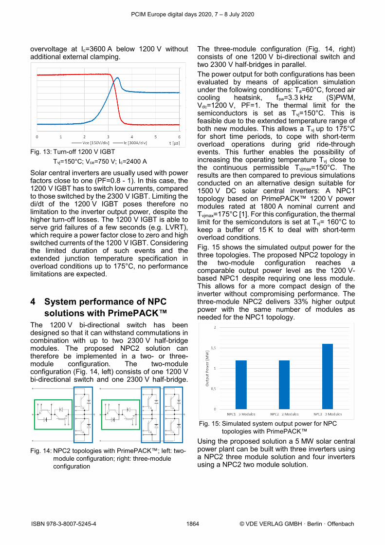
The 1200 V bi-directional switch has been designed so that it can withstand commutations in combination with up to two 2300 V half-bridge modules. The proposed NPC2 solution can therefore be implemented in a two- or three-module configuration. The two-moduleconfiguration (Fig. 14, left) consists of one 1200 Vbi-directional switch and one 2300 V half-bridge.
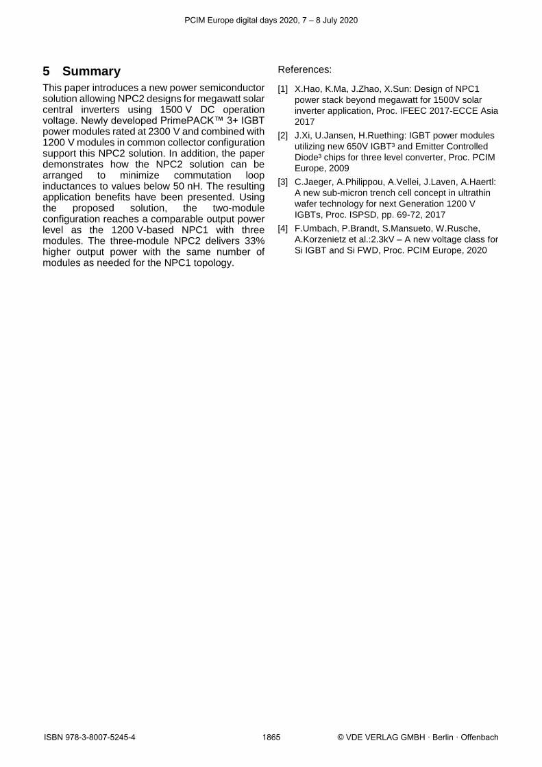
The three-module configuration (Fig. 14, right)consists of one 1200 V bi-directional switch and two 2300 V half-bridges in parallel.The power output for both configurations has been evaluated by means of application simulation under the following conditions: Ta=60°C, forced aircooling heatsink, fsw=3.3 kHz (S)PWM,Vdc=1200 V, PF=1. The thermal limit for the semiconductors is set as Tvj=150°C. This is feasible due to the extended temperature range of both new modules. This allows a Tvj up to 175°C for short time periods, to cope with short-term overload operations during grid ride-through events. This further enables the possibility ofincreasing the operating temperature Tvj close to the continuous permissible Tvjmax=150°C. The results are then compared to previous simulations conducted on an alternative design suitable for 1500 V DC solar central inverters: A NPC1 topology based on PrimePACK™ 1200 V power modules rated at 1800 A nominal current and Tvjmax=175°C [1]. For this configuration, the thermal limit for the semicondutors is set at Tvj= 160°C to keep a buffer of 15 K to deal with short-termoverload conditions.Fig. 15 shows the simulated output power for the three topologies. The proposed NPC2 topology inthe two-module configuration reaches acomparable output power level as the 1200 V-based NPC1 despite requiring one less module. This allows for a more compact design of the inverter without compromising performance. The three-module NPC2 delivers 33% higher output power with the same number of modules as needed for the NPC1 topology.
Using the proposed solution a 5 MW solar central power plant can be built with three inverters using a NPC2 three module solution and four inverters using a NPC2 two module solution.
Fig. 14: NPC2 topologies with PrimePACK™; left: two-module configuration; right: three-module configuration
Fig. 13: Turn-off 1200 V IGBTTvj=150°C; Vce=750 V; Ic=2400 A
Fig. 15: Simulated system output power for NPC topologies with PrimePACK™
PCIM Europe digital days 2020, 7 – 8 July 2020
ISBN 978-3-8007-5245-4 © VDE VERLAG GMBH · Berlin · Offenbach1864
5 Summary
This paper introduces a new power semiconductor solution allowing NPC2 designs for megawatt solar central inverters using 1500 V DC operation voltage. Newly developed PrimePACK™ 3+ IGBT power modules rated at 2300 V and combined with 1200 V modules in common collector configuration support this NPC2 solution. In addition, the paper demonstrates how the NPC2 solution can be arranged to minimize commutation loop inductances to values below 50 nH. The resulting application benefits have been presented. Using the proposed solution, the two-module configuration reaches a comparable output power level as the 1200 V-based NPC1 with three modules. The three-module NPC2 delivers 33% higher output power with the same number of modules as needed for the NPC1 topology.
References:
[1] X.Hao, K.Ma, J.Zhao, X.Sun: Design of NPC1
power stack beyond megawatt for 1500V solar
inverter application, Proc. IFEEC 2017-ECCE Asia
2017
[2] J.Xi, U.Jansen, H.Ruething: IGBT power modules
utilizing new 650V IGBT³ and Emitter Controlled
Diode³ chips for three level converter, Proc. PCIM
Europe, 2009
[3] C.Jaeger, A.Philippou, A.Vellei, J.Laven, A.Haertl:
A new sub-micron trench cell concept in ultrathin
wafer technology for next Generation 1200 V
IGBTs, Proc. ISPSD, pp. 69-72, 2017
[4] F.Umbach, P.Brandt, S.Mansueto, W.Rusche,
A.Korzenietz et al.:2.3kV – A new voltage class for
Si IGBT and Si FWD, Proc. PCIM Europe, 2020
PCIM Europe digital days 2020, 7 – 8 July 2020
ISBN 978-3-8007-5245-4 © VDE VERLAG GMBH · Berlin · Offenbach1865
Related Documents