Visit analog.com IN THIS ISSUE April 2018 Volume 1 Number 2 Power Management Journal of automotive USB Type-C power solution 12 triple bucks plus a boost controller for automotive applications 16 LED driver for high power machine vision flash 20 dual channel monolithic synchronous step-down Silent Switcher 2 regulator 28 60V and 100V, Low I Q Boost/SEPIC/ Inverting Converters for Compact, Efficient, Low EMI Power Supplies Joey Yurgelon , Jesus Rosales and Mark Marosek Automotive and industrial markets demand cool running power supplies that fit tight spaces and meet low EMI standards. The LT8362, LT8364 and LT8361 switching regulators meet these demands in boost, SEPIC or inverting topologies. Each supports a wide 2.8V to 60V input range, for industrial or automotive environments, low I Q Burst Mode capability and optional SSFM for reduced EMI. With built-in rugged power switches of 60V/2A, 60V/4A and 100V/2A, including efficient operation up to 2MHz, these devices can deliver high power in small spaces while meeting stringent thermal and EMI requirements. AUTOMOTIVE INPUT TRANSIENTS AND PRE-BOOST With the dramatic increase of electronic content in today’s automobiles, the number of power supplies has multiplied, with many required to directly convert a wide-ranging battery voltage to a usable, regulated output. With a minimum input voltage of 2.8V, all members of the LT836x family can operate during cold crank or stop-start events; the maximum input voltage (continued on page 4) With 10,000:1 dimming, the LT3932 buck LED driver makes cutting edge applications possible. (See page 20.)

Welcome message from author
This document is posted to help you gain knowledge. Please leave a comment to let me know what you think about it! Share it to your friends and learn new things together.
Transcript

Visit analog.com
I N T H I S I S S U E
April 2018 Volume 1 Number 2
Power ManagementJournal of
automotive USB Type-C
power solution 12
triple bucks plus a boost
controller for automotive
applications 16
LED driver for high power
machine vision flash 20
dual channel monolithic
synchronous step-down
Silent Switcher 2 regulator
28
60V and 100V, Low IQ Boost/SEPIC/Inverting Converters for Compact, Efficient, Low EMI Power SuppliesJoey Yurgelon , Jesus Rosales and Mark Marosek
Automotive and industrial markets demand cool running power supplies that fit tight spaces and meet low EMI standards. The LT8362, LT8364 and LT8361 switching regulators meet these demands in boost, SEPIC or inverting topologies. Each supports a wide 2.8V to 60V input range, for industrial or automotive environments, low IQ Burst Mode capability and optional SSFM for reduced EMI. With built-in rugged power switches of 60V/2A,
60V/4A and 100V/2A, including efficient operation up to 2MHz, these devices can deliver high power in small spaces while meeting stringent thermal and EMI requirements.
AUTOMOTIVE INPUT TRANSIENTS AND PRE-BOOST
With the dramatic increase of electronic content
in today’s automobiles, the number of power
supplies has multiplied, with many required to
directly convert a wide-ranging battery voltage
to a usable, regulated output. With a minimum
input voltage of 2.8V, all members of the
LT836x family can operate during cold crank or
stop-start events; the maximum input voltage
(continued on page 4)With 10,000:1 dimming, the LT3932 buck LED driver makes cutting edge applications possible. (See page 20.)

2 | April 2018 : Power by Linear Journal of Power Management
In this issue...
POWER DEMOS SHOWN AT APEC 2018
The ADI Power by Linear™ group was at APEC 2018 (Applied
Power Electronics Conference in San Antonio, Texas in March)
with a team of power experts to showcase innovative power
technologies. The demonstrations presented at APEC included:
•High power isolated gate driver board for Microsemi
half-bridge SiC power module
•Hot Swap and power management
•Power over Ethernet
•Power system management (see Spotlight below)
•Wireless power for industrial and medical handheld
devices and hearing aids (see Spotlight below)
•USB-C power delivery battery charger featuring the LTC4162
•Power µModule® solutions are simple & done
•Low electromagnetic emissions benefits of Silent Switchers
SPOTLIGHT ON APEC 2018: PSM & WIRELESS POWER
Power System Management (PSM), Hot Swap & LTpowerPlay
Mike Jones’ demonstration at APEC provided a live, interactive experience of the
Total Managed Power demo board (DC2578A) and the LTpowerPlay software.
Power System Management ICs give designers vast digital control of system
power rails. LTpowerPlay is a PC-based graphical interface that allows
designers to monitor and program the complete power system, from
Hot Swap, through intermediate buses, to point-of-load controllers.
The PSM family provides extremely accurate configurable power regu-
lation, configurable safety limits, coordinated fault responses, a full
suite of live telemetry, a rich set of configuration and control encapsu-
lated in EEPROM memory, and a comprehensive software tool that brings
together all of these features and ICs. PSM solutions provide:
•Extreme accuracy
•High reliability and safety
•Autonomous operation
•Complete telemetry and status information
•High system configurability across any number of supply rails
Open Circuit
COVER STORY
60V and 100V, Low IQ Boost/SEPIC/Inverting Converters for Compact, Efficient, Low EMI Power SuppliesJoey Yurgelon , Jesus Rosales and Mark Marosek 1
DESIGN FEATURES
Automotive USB Type-C Power Solution: 45W, 2MHz Buck-Boost Controller in 1-Inch SquareKyle Lawrence 12
Triple Bucks Plus a Boost Controller to Meet Tough Requirements of Wide Range VIN Automotive ApplicationsZhongming Ye 16
DESIGN IDEAS
LED Driver for High Power Machine Vision FlashKyle Lawrence and Keith Szolusha 20
1000V Output, No-Opto Isolated Flyback ConverterGeorge Qian, Michael Wu 23
40V Input, 3.5A Silent Switcher µModule Regulator for Automotive and Industrial ApplicationsZhongming Ye 25
Dual Channel 42V, 4A Monolithic Synchronous Step-Down Silent Switcher 2 with 6.2µA Quiescent CurrentHua (Walker) Bai 28
Active Rectifier Controller with Ultrafast Transient Response and Low Power DissipationBin Wu 30
back page circuits 32

April 2018 : Power by Linear Journal of Power Management | 3
open circuit
Wireless Battery Chargers for Hearing Aid and Handheld Applications
Brian Shaffer (Applications Engineering
Manager for Analog Devices Power
Business) demonstrated wireless
battery charging solutions for hearing
aids and handheld applications.
25mA Wireless NiMH Charger for Hearing
Aid Applications—On display was the
LTC4123, a complete 1.5V, 25mA, NiMH wireless battery charger. The LTC4123
features a temperature-compensated
charge voltage, an integrated rectifier
with overvoltage limit, zinc-air primary
battery detection and reverse polarity
protection. A complete solution
comprising the 2mm × 2mm LTC4126
and four additional components fits
on a PCB with less than 6mm diameter,
ideal for hearing aid applications.
Hearing Aid Wireless Charging and DC/DC Power:
7.5mA Wireless Li-Ion Charger & 1.2V/60mA
DC/DC—Shaffer also demonstrated the
LTC4126 wireless 7.5mA Li-ion battery
charger with integrated high efficiency
1.2V, 60mA multimode DC/DC charge
pump. The LTC4126 is perfectly suited
for hearing aid applications because of
its extremely small solution size and
numerous protection features, such as:
•Integrated rectifier with overvoltage
limit
•Pin-selectable charge voltages of 4.2V or
4.35V
•3V low battery disconnect
•NTC pin for temperature qualified
charging
•6-hour termination timer
The LTC4126 is offered in a thermally
enhanced 2mm × 2mm LQFN package.
The charge pump output is designed
to duplicate the load profile of a
NiMH battery so that existing hearing
aid ASICS can be powered directly,
without additional conversion.
Battery Charger Receiver and Transmitter
Combination for Higher Power Industrial Handheld
Solutions—For industrial handheld
applications, Brian demonstrated the
LTC4120 battery charger receiver and
the LTC4125 transmitter combination.
The LTC4120 is a wireless power receiver
and 400mA buck battery charger with
dynamic harmonization control, which
optimizes wireless charging over a wide
coupling gap. It can charge single or
multiple series lithium-ion batteries
and is offered in a thermally enhanced,
16-lead 3mm × 3mm QFN package.
The LTC4125, 5W AutoResonant™
wireless power transmitter works seam-
lessly with the LTC4120. The LTC4125’s
switching frequency adjusts to changes
in resonant capacitance and transmit coil
inductance. The LTC4125 reduces power
dissipation by automatically adjusting its
transmit power to the receiver load. It has
multiple foreign object detection methods,
programmable average input current limit
and an NTC input for system component
temperature-qualified power transfer. n
The Power by Linear group presented a variety of industry-specific power solutions at APEC 2018
VIN
LTXLRX 8µH
CRX68nF
2.2µF1.2V
TRANSMITTER
AIR GAP
ACIN
OUTVSEL
GND
Li-Ion4.2V
LTC4126 BAT
NTCCHRG
VCC
+–
+
ACPRSTAT2
DIGITAL I/OSTAT1
EN
TO BAT
The LTC4126 for hearing aid applicatins was demonnstrated at APEC 2018
4 | April 2018 : Power by Linear Journal of Power Management
of applications. The high power switch
voltage ratings of the LT836x family extend
output voltage capability in addition
to extending the input voltage range
for SEPICs and inverting converters.
capability of up to 60V handles high input
voltage transients such as load dump.
This wide input voltage range makes
the LT836x family ideal for automo-
tive pre-boost applications. Automotive
buck regulators require a pre-boost
stage in applications where battery input
voltage can drop below the buck output
voltage. The LT8361, LT8362 and LT8364
provide the necessary boosting during
low battery levels, and turn off with
minimal power consumption during
normal or load dump battery voltages.
RUGGED POWER SWITCHES
A key requirement for any switching
regulator is to provide enough power
for a given application over the entire
input voltage range while also guaran-
teeing reliability. Rugged power switches
with voltage/peak current offerings of
60V/2A (LT8362), 60V/4A (LT8364) and
100V/2A (LT8361) enable a wide range
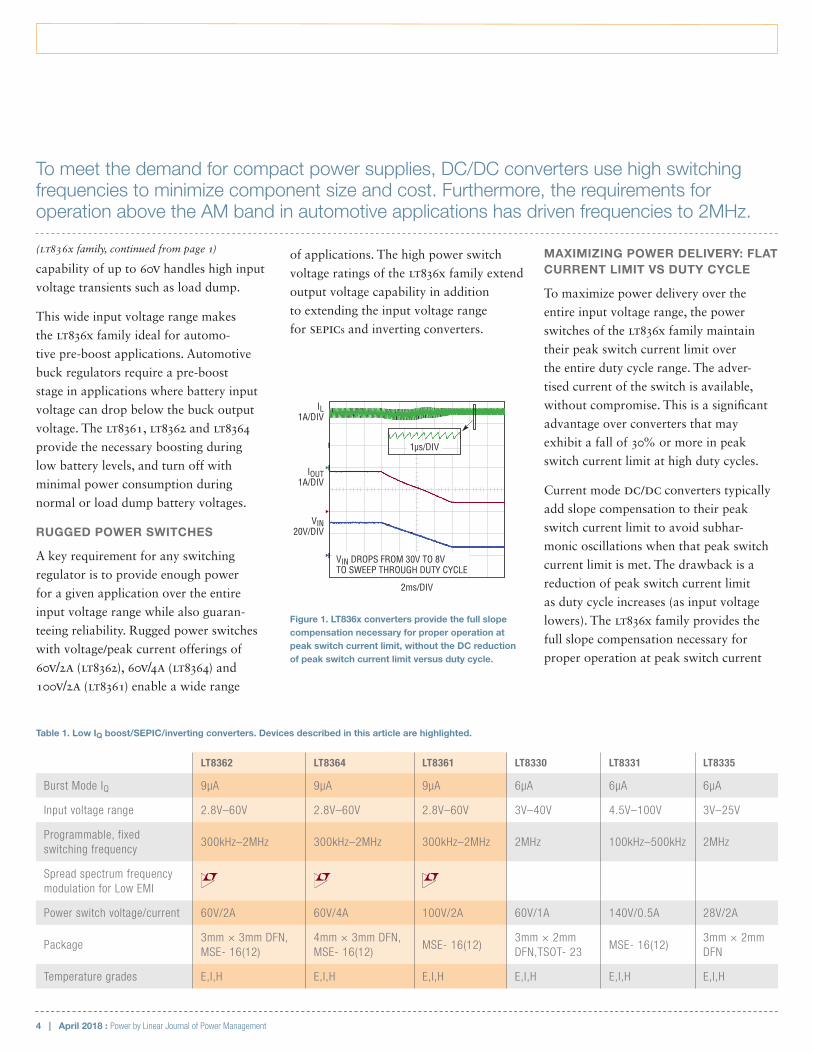
MAXIMIZING POWER DELIVERY: FLAT CURRENT LIMIT VS DUTY CYCLE
To maximize power delivery over the
entire input voltage range, the power
switches of the LT836x family maintain
their peak switch current limit over
the entire duty cycle range. The adver-
tised current of the switch is available,
without compromise. This is a significant
advantage over converters that may
exhibit a fall of 30% or more in peak
switch current limit at high duty cycles.
Current mode DC/DC converters typically
add slope compensation to their peak
switch current limit to avoid subhar-
monic oscillations when that peak switch
current limit is met. The drawback is a
reduction of peak switch current limit
as duty cycle increases (as input voltage
lowers). The LT836x family provides the
full slope compensation necessary for
proper operation at peak switch current
(LT836x family, continued from page 1)
To meet the demand for compact power supplies, DC/DC converters use high switching frequencies to minimize component size and cost. Furthermore, the requirements for operation above the AM band in automotive applications has driven frequencies to 2MHz.
Table 1. Low IQ boost/SEPIC/inverting converters. Devices described in this article are highlighted.
LT8362 LT8364 LT8361 LT8330 LT8331 LT8335
Burst Mode IQ 9µA 9µA 9µA 6µA 6µA 6µA
Input voltage range 2.8V–60V 2.8V–60V 2.8V–60V 3V–40V 4.5V–100V 3V–25V
Programmable, fixed switching frequency
300kHz–2MHz 300kHz–2MHz 300kHz–2MHz 2MHz 100kHz–500kHz 2MHz
Spread spectrum frequency modulation for Low EMI
Power switch voltage/current 60V/2A 60V/4A 100V/2A 60V/1A 140V/0.5A 28V/2A
Package3mm × 3mm DFN, MSE- 16(12)
4mm × 3mm DFN, MSE- 16(12)
MSE- 16(12)3mm × 2mm DFN,TSOT- 23
MSE- 16(12)3mm × 2mm DFN
Temperature grades E,I,H E,I,H E,I,H E,I,H E,I,H E,I,H
2ms/DIV
IOUT1A/DIV
VIN20V/DIV
IL1A/DIV
1µs/DIV
VIN DROPS FROM 30V TO 8VTO SWEEP THROUGH DUTY CYCLE
Figure 1. LT836x converters provide the full slope compensation necessary for proper operation at peak switch current limit, without the DC reduction of peak switch current limit versus duty cycle.

April 2018 : Power by Linear Journal of Power Management | 5
design features
limit, without the DC reduction of peak
switch current limit versus duty cycle.
2MHz OPERATION: COMPACT POWER SUPPLIES, ABOVE AM BAND
To meet the demand for compact
power supplies, DC/DC converters use
high switching frequencies to minimize
component size and cost. Furthermore,
the requirements for operation above
the AM band in automotive applica-
tions has driven frequencies to 2MHz.
Traditionally, high switching frequencies
result in increased switching losses and
limited duty cycle range. The LT836x
family minimizes AC switching losses using
fast power switch drivers and features
low minimum on- and off-times, enabling
support of a wide conversion range even
at 2MHz. For instance, the LT836x family
can achieve lower losses and a higher
duty cycle range than many applications
that would traditionally run at 400kHz to
maximize efficiency. Thermal performance
for each of the covered topologies—boost,
SEPIC and inverting—is shown in Figure 2.
Traditionally, high switching frequencies result in increased switching losses and limited duty cycle range. The LT836x family minimizes AC switching losses using fast power switch drivers and features low minimum on- and off-times, enabling support of a wide conversion range even at 2MHz.
Figure 2. Thermal performance of LT8362 Cuk inverting, LT8364 boost and LT8361 SEPIC solutions.
CukVIN = 12VVOUT = −12VIOUT = 750mA2MHz OPERATION
(a) LT8362 DC2517A inverting converter
BOOSTVIN = 12VVOUT = 24VIOUT = 1.2A2MHz OPERATION
(b) LT8364 DC2716A boost converter
SEPICVIN = 12VVOUT = 24VIOUT = 450mA400kHz OPERATION
(c) LT8361 DC2599A SEPIC converter
Figure 3. Compact, EMI friendly converter solutions
(a) LT8362 low EMI inverting converter (b) LT8364 low EMI boost converter (c) LT8361 low EMI SEPIC converter

6 | April 2018 : Power by Linear Journal of Power Management
BURST MODE OPERATION: HIGH EFFICIENCY AT LIGHT LOAD
High efficiency at light loads is a critical
feature in automotive environments where
extending battery life is of utmost impor-
tance. The LT836x family offers high effi-
ciency at light loads with optional Burst
Mode® operation—selectable using the
SYNC/MODE pin (see Table 2.). Burst Mode
operation uses single-switch pulses spaced
evenly at a lower switching frequency
to reduce switching losses, while mini-
mizing output voltage ripple. The LT836x
family can draw as little as 9µA from the
input pin when in deep sleep or in pass
through mode in a pre-boost application.
SSFM MODE: THREE TOPOLOGIES PASSING CISPR 25 CLASS 5
The LT836x family is capable of
meeting CISPR 25 Class 5 standards
using spread spectrum frequency
modulation (SSFM) mode and proper
board layout with some filtering.
Designers have traditionally avoided using
switching regulators throughout EMI sensitive environments. A switcher’s large
capacitors and troublesome hot loops
elevate the importance of PCB layout to
achieve good EMI performance and small
solution size, placing a burden on board
design and manufacture. The available
factory demonstration circuits for the
LT8362, LT8364 and LT8361 include the
requisite input/output filters and feature
exemplary PCB layout to meet CISPR 25
Class 5 standards (as tested) when SSFM
SYNC/MODE PIN INPUT CAPABLE MODES OF OPERATION
(1) GND or < 0.14V Burst Mode operation
(2) External clock Pulse-skipping/sync
(3) 100k resistor to GND Burst/SSFM
(4) Float (pin open) Pulse-skipping
(5) INTVCC or > 1.7V Pulse-skipping/SSFM
FREQUENCY (MHz)0.1 1 10 30
–20
–12
–4
4
12
20
28
36
44
52
60
AVG
COND
UCTE
D (d
BµV)
12V INPUT TO 24V OUTPUT AT 1A, fSW = 2MHz, SSFM ON
CLASS 5 AVERAGE LIMITMEASURED EMISSIONS
FREQUENCY (MHz)0.1 1 10 30
–20
–10
0
10
20
30
40
50
60
70
80CLASS 5 PEAK LIMITMEASURED EMISSIONS
12V INPUT TO 24V OUTPUT AT 1A, fSW = 2MHz, SSFM ON
PEAK
CON
DUCT
ED (d
BµV)
12V INPUT TO 24V OUTPUT AT 1A, fSW = 2MHz, SSFM ON
FREQUENCY (MHz)0 100 200 300 400 500 600 700 800 900 1000
–20
–10
0
10
20
30
40
50
60
PEAK
RAD
IATE
D (d
BµV/
m)
CLASS 5 PEAK LIMITMEASURED EMISSIONS
FREQUENCY (MHz)0 100 200 300 400 500 600 700 800 900 1000
–20
–10
0
10
20
30
40
50
60
AVG
RADI
ATED
(dBµ
V/m
)
CLASS 5 AVERAGE LIMITMEASURED EMISSIONS
12V INPUT TO 24V OUTPUT AT 1A, fSW = 2MHz, SSFM ON
Figure 4. EMI test results for LT8364 boost solution
Table 2. LT836x family capable modes of operation

April 2018 : Power by Linear Journal of Power Management | 7
design features
BEST OF BOTH: BURST MODE OPERATION & SSFM
Until recently, selecting SSFM mode for low
EMI meant having to use the less efficient
pulse-skipping mode at light load, but the
LT836x family does not require this trade-
off. By simply adding a 100k resistor from
SYNC/MODE pin to ground (see Table 2),
mode is selected (see Table 2). By essen-
tially removing the converter from the
EMI equation, application development
time and cost are reduced. Figure 4 shows
EMI test results for a boost solution.
the LT836x family seamlessly transitions
from SSFM mode to Burst Mode operation
when loads become light. The result is low
EMI and high efficiency over all loads.
PACKAGES, PIN COMPATIBILITY AND TEMPERATURE GRADES
For customers who prefer leaded
packages, each part is offered in a pin-
compatible MSE16(12) TSSOP with four
pins removed for HV pin spacing. For
a smaller solution size, the LT8362 and
LT8364 are also offered in DFN packages.
The LT8362 (3mm × 3mm) DFN(10)
is pin compatible with the LT8364 by
placing it onto the (4mm × 3mm) LT8364
DFN(12) PCB space (see Figure 6). All
packages include a thermally enhanced
exposed ground pad and are offered
in E, I and H temperature grades.
Until recently, selecting SSFM mode for low EMI meant using the less efficient pulse-skipping mode at light load. The LT836x family does not require this trade-off.
Figure 5. Pulse-skipping vs Burst Mode operation for LT8362 boost solution (24V input to 48V output)
Burst Mode OPERATIONPULSE-SKIPPING
LOAD CURRENT (A)0.001 0.01 0.1 10
10
20
30
40
50
60
70
80
90
100
EFFI
CIEN
CY (%
)
VIN = 24VVOUT = 48V
(a) Pulse-skipping and Burst Mode operation light load efficiency
LOAD CURRENT (A)0.0001 0.001 0.01 0.1 10
1
2
3
4
5
6
V IN
PIN
CURR
ENT
(mA)
Burst Mode OPERATIONPULSE-SKIPPING
VIN = 24VVOUT = 48V
(b) Pulse-skipping and Burst Mode operation light load VIN pin current
1 3 5678
EN/UVLO
VIN
INTVCCNC
BIASVC
16 14 1211109
SW1
SW2 SYNC/MODESSRTFBX
TOP VIEW
17PGND,
GND
MSE PACKAGEVARIATION: MSE16 (12)16-LEAD PLASTIC MSOP
TOP VIEW
DD PACKAGE10-LEAD (3mm × 3mm) PLASTIC DFN
10
9
6
7
8
4
5
3
2
1 SW
SYNC/MODE
SS
RT
FBX
EN/UVLO
VIN
INTVCC
BIAS
VC
11PGND,GND
12
11
10
9
8
7
13GND
1
2
3
4
5
6
SW1
SW2
SYNC/MODE
SS
RT
FBX
NC
EN/UVLO
VIN
INTVCC
BIAS
VC
TOP VIEW
DE PACKAGE12-LEAD (4mm × 3mm) PLASTIC DFN
PIN COMPATIBLE
LT8361(100V/2A)LT8362 (60V/2A)LT8364 (60V/4A)
LT8362 LT8364
PIN COMPATIBLE FOR PCB
Figure 6. Pin compatiblity of packages for the LT8361, LT8362 and LT8364

8 | April 2018 : Power by Linear Journal of Power Management
By offering a single FBX pin that allows for both positive and negative output voltages, all topologies are within reach. An inverting application is just as accessible as that of a boost or SEPIC, reducing design time and effort.
VIN = 12VVIN = 24V
LOAD CURRENT (A)0 0.1 0.2 0.3 0.4 0.5 0.6 0.7 0.8 0.9 1.0 1.1
50
60
70
80
90
100
EFFI
CIEN
CY (%
)
VOUT = 24V
D1
1MEG10µF25V
1206
71.5k
1µF20k
2MHz 0.22µF2.2nF
22.1k
L12.2µH
10µF50V1210
C633µF50V
0.1µF50V0402
100k
4.7µF25V
1206
0.1µF×250V0402
0.1µF50V0402
VIN
FBX
BIAS
GND
EN/UVLO
LT8364
D1: DIODES INC. DFLS260L1: WÜRTH ELEKTRONIK LHMI 74437324022L2: WÜRTH ELEKTRONIK 74479299147FB1: WÜRTH ELEKTRONIK 742792040C6: 50CE33PCS
SW
SYNC/MODE INTVCC
RT SS VC
INPUT EMI FILTERL2
0.47µHOUTPUT EMI FILTER
FB1VIN5V TO 20V
VOUT24V600mA AT VIN = 5V1.4A AT VIN= 12V
Figure 7. LT8364, 2MHz, 24V output boost converter passes CISPR 25 Class 5 EMI (see Figure 4).
10µF50V
1206
4.7µF50V
1206×2
1µF
6.8nF
0.22µF
1M
71.5k
16.2k121k400kHz
D1
C1410µF50V1210
L1A22µH
L1B22µH
1µF100V1206
C268µF50V
0.1µF35V0402×2
0.1µF35V0402
0.1µF35V0402
100k
INPUT EMI FILTERL2
470nHOUTPUT EMI FILTER
FB2
EN/UVLO
RT
VIN SW
FBX
BIAS
INTVCC
SS GND VC
LT8361SYNC/MODE
D1: DIODES INC. DFLS2100L1: WURTH ELEKTRONIK WE-DD 7345 744877220L2: WURTH ELEKTRONIK 74479876147C2: PANASONIC EEHZC1H680PC14: MURATA GRM32ER71H106KA12LFB2: WURTH ELEKTRONIK 742792040
VIN5V TO 48V
VOUT24V
VOUT
VIN = 12VVIN = 48V
LOAD CURRENT (A)0 0.1 0.2 0.3 0.4 0.5 0.6 0.7
50
55
60
65
70
75
80
85
90
95
100
EFFI
CIEN
CY (%
)
VOUT = 24VFigure 8. LT8361, 400kHz, 24V output SEPIC converter passes CISPR 25 Class 5 EMI

April 2018 : Power by Linear Journal of Power Management | 9
design features
BOOST/SEPIC/INVERTING: FBX PIN FOR POSITIVE OR NEGATIVE OUTPUTS
By offering a single FBX pin that allows
for both positive and negative output
voltages, all topologies are within
reach. An inverting application is just as
accessible as that of a boost or SEPIC, reducing design time and effort.
Boost Converters
For applications requiring output voltages
greater than the input, the LT836x family
is ideal for many boost converter appli-
cations given the 2.8V-to-60V input
capability and range of power switch
ratings. For large conversion ratio designs,
operating in discontinuous conduction
mode (DCM) might be the best solution;
continuous conduction mode (CCM) can deliver higher output power.
The converter in Figure 7 shows
an LT8364 low IQ, low EMI, 2MHz,
24V boost converter with SSFM that
passes CISPR 25 Class 5 radiated and
conducted EMI (Figure 4). With an
input of 12V, this application easily
reaches a peak efficiency of 94%.
FREQUENCY (MHz)0.1 1 10 30
–40
–30
–20
–10
0
10
20
30
40
50
60
AVER
AGE
COND
UCTE
D EM
I (dB
µV)
CLASS 5 AVERAGE LIMITMEASURED EMISSIONS
12V INPUT TO 24V OUTPUT AT 500mA, fSW = 400kHz, SSFM ON
12V INPUT TO 24V OUTPUT AT 500mA, fSW = 400kHz, SSFM ON
CLASS 5 PEAK LIMITMEASURED EMISSIONS
FREQUENCY (MHz)0.1 1 10 30
–20
–10
0
10
20
30
40
50
60
70
80
PEAK
CON
DUCT
ED E
MI (
dBµV
)
FREQUENCY (MHz)0 100 200 300 400 500 600 700 800 900 1000
–20
–10
0
10
20
30
40
50
60
PEAK
RAD
IATE
D EM
I (dB
µV/m
)
12V INPUT TO 24V OUTPUT AT 500mA, fSW = 400kHz, SSFM ON
CLASS 5 PEAK LIMITMEASURED EMISSIONS
CLASS 5 AVERAGE LIMITMEASURED EMISSIONS
FREQUENCY (MHz)0 100 200 300 400 500 600 700 800 900 1000
–20
–10
0
10
20
30
40
50
60
AVER
AGE
RADI
ATED
EM
I (dB
µV/m
)
12V INPUT TO 24V OUTPUT AT 500mA, fSW = 400kHz, SSFM ON
Figure 9. EMI test results for LT8361 SEPIC solution
For applications requiring output voltages greater than the input, the LT836x family is ideal for many boost converter applications given the 2.8V-to-60V input capability and range of power switch ratings. For large conversion ratio designs, operating in discontinuous conduction mode (DCM) might be the best solution; continuous conduction mode (CCM) can deliver higher output power.

10 | April 2018 : Power by Linear Journal of Power Management
SEPIC Converters
Automotive and industrial applications
often operate from input voltages that
can be above and below the required
output voltage. For applications where
the DC/DC converter is required to both
step-up and step-down its input, a SEPIC topology is often the solution. SEPICs
support applications that require output
disconnect, ensuring no output voltage
during shutdown and tolerating output
short-circuit faults since there is no DC path from input to output. With switch
ratings of 60V/100V, and low minimum
on- and off-times, wide input voltage
ranges are achievable. The LT836x family
offers an optional BIAS pin which serves
as a second input supply for the INTVCC regulator for improved efficiency.
The SEPIC converter in Figure 8 uses the
LT8361 to showcase the versatility of a
100V rated switch. The switch voltage
rating must be greater than the addition
of maximum input and output voltages.
With a 48V input to 24V output, the
switch can easily handle the required 72V. With use cases where the input is greater
than the output, the BIAS pin can offer
improved efficiency when connected to
VOUT. Operating with SSFM, this applica-
tion passes CISPR 25 Class 5 radiated
and conducted EMI (Figure 9). Peak
efficiency with a 12V input is 88%.
Inverting Converters
Negative supplies are commonly used in
today’s electronics. However, many appli-
cations only have a positive input voltage
from which to operate. The LT836x family,
when configured in the inverting topology,
can regulate from a positive input voltage
that is above or below the magnitude of
the negative output voltage. As with the
SEPIC topology, the high 60V/100 switch
ratings and low minimum on- and off-
times allow wide input voltage ranges.
Operating at 2MHz, the LT8362 offers
an easy way to create a negative voltage
from a positive input supply, as shown
in Figure 10—a low IQ, low EMI, 2MHz, –12V inverting converter with
SSFM. With the rugged 60V switch, this
10µF50V
1206
0.1µF100V0402
0.1µF100V0402
4.7µF50V
1206
1µF
1.5nF0.22µF
1M
71.5k
40.2k20k2MHz
D110µF50V1210
L1A6.8µH
L1B6.8µH
1µF100V1206
C233µF50V
1206
100k
0.1µF100V0402×2
1µF50V
0603
INPUT EMI FILTERL2
470nHOUTPUT EMI FILTER
FB2
EN/UVLO
RT
VIN SW
FBX
BIAS
INTVCC
SS GND VC
LT8362
SYNC/MODE D1: DIODES INC. DFLS260L1: WÜRTH ELEKTRONIK WE-DD 74489430068L2: WÜRTH ELEKTRONIK 74479876147C2: 50CE33PCSFB2: WÜRTH ELEKTRONIK 742792040
VIN4.5V TO 42V
VOUT–12V
CURRENT (mA)0 100 200 300 400 500 600 700 800 900 1000
40
50
60
70
80
90
EFFI
CIEN
CY (%
)
VOUT = –12V
VIN = 5VVIN = 12VVIN = 24V
Figure 10. LT8362, 2MHz, −12V output, inverting converter passes CISPR 25 Class 5 EMI.
For applications where the DC/DC converter is required to both step-up and step-down its input, a SEPIC topology is often the solution. SEPICs support applications that require output disconnect, ensuring no output voltage during shutdown and tolerating output short-circuit faults since there is no DC path from input to output.

April 2018 : Power by Linear Journal of Power Management | 11
design features
application can operate with inputs up
to 42V (|VOUT| + VIN < 60V). With a VIN
of 12V, a peak efficiency of 85% can be
achieved. Operating with SSFM, this
application passes CISPR 25 Class 5
radiated and conducted EMI (Figure 11).
CONCLUSION
To satisfy the automotive and industrial
market demand for compact, efficient, low
EMI power supplies, the LT836x family
provides the rugged LT8362 (60V/2A), LT8364 (60V/4A) and LT8361 (100V/2A)
switching regulators for boost, SEPIC and
inverting topologies. These devices are
a significant improvement over alterna-
tives due to low IQ Burst Mode operation,
flat switch current limit over duty cycle,
low loss switching for 2MHz operation
and a wide 2.8V to 60V input range.
Low EMI performance is achieved
through proper demo board layout
and filter design with SSFM mode to
meet CISPR 25 Class 5 EMI standards.
Design development is simplified with
MSE16(12) pin compatibility for all parts
and footprint compatibility for LT8362
(3mm × 3mm DFN(10)) and LT8364
(4mm × 3mm DFN(12)). All members
of the LT836x family are available in
E, I, and H temperature grades. n
To satisfy the automotive and industrial market demand for compact, efficient, low EMI power supplies, the LT836x family provides the rugged LT8362 (60V/2A), LT8364 (60V/4A) and LT8361 (100V/2A) switching regulators for boost, SEPIC and inverting topologies.
12V INPUT TO –12V OUTPUT AT 600mA, fSW = 2MHz, SSFM ON
CLASS 5 AVERAGE LIMITMEASURED EMISSIONS
FREQUENCY (MHz)0.1 1 10 30
–20
–12
–4
4
12
20
28
36
44
52
60
AVG
COND
UCTE
D (d
BµV)
FREQUENCY (MHz)0.1 1 10 30
–20
–10
0
10
20
30
40
50
60
70
80
PEAK
CON
DUCT
ED (d
BµV)
CLASS 5 PEAK LIMITMEASURED EMISSIONS
12V INPUT TO –12V OUTPUT AT 600mA, fSW = 2MHz, SSFM ONCLASS 5 PEAK LIMITMEASURED EMISSIONS
FREQUENCY (MHz)0 100 200 300 400 500 600 700 800 900 1000
–20
–10
0
10
20
30
40
50
60
PEAK
RAD
IATE
D (d
BµV/
m)
12V INPUT TO –12V OUTPUT AT 600mA, fSW = 2MHz, SSFM ON
FREQUENCY (MHz)0 100 200 300 400 500 600 700 800 900 1000
–20
–10
0
10
20
30
40
50
60
CLASS 5 AVERAGE LIMITMEASURED EMISSIONS
AVG
RADI
ATED
(dBµ
V/m
)
12V INPUT TO –12V OUTPUT AT 600mA, fSW = 2MHz, SSFM ON
Figure 11. EMI test results for LT8362 inverting solution

12 | April 2018 : Power by Linear Journal of Power Management
95% EFF
45W
TYPE C
PR
ND
CD-IN Bluetooth
PASSENGER
AIR BAG
OFF
SETUP
BLUELINK
APPS
TRACK
SEEK
PHONE
A/C
MEDIA
AUTOOFF
REAR
FRONT
SYNC
A/C
ECON
MODE
DRIVER
ONLY
AUX
12V
12V
CHARGING
Automotive USB Type-C Power Solution: 45W, 2MHz Buck-Boost Controller in 1-Inch SquareKyle Lawrence
The simple, compact buck regulators and
linear regulators used in battery chargers
that require only USB 5V at 500mA–2A do not sufficiently cover the full range
of Type-C USB power. The increased
voltage range, 5V–20V, of Type-C USB power delivery requires more than just
step-down voltage conversion from
9V–36V (or 60V) automotive batteries,
or other charging sources. An adjustable
buck-boost converter is needed with
the ability to both step-up and step-
down the input-to-output voltage.
Additionally, for high power automotive
USB chargers, a buck-boost converter
should support a 10A or higher peak
switch current rating and offer low
EMI performance. The ability to set
the switching frequency outside the
AM radio band and maintain a small
solution size are sought-after features.
High voltage monolithic converters
(with onboard switches) are not
capable of sustaining such high peak
switch currents without burning up.
The LT8390A is a unique 2MHz synchro-
nous 4-switch buck-boost controller. At
2MHz switching frequency, it can deliver
output voltages between 5V and 15V (up
to 45W at 3A), to provide power to a
connected USB-C device from a car battery.
This high controller switching frequency
keeps the solution size small, the band-
width high, and the EMI outside of the
AM radio band. Both spread spectrum
frequency modulation and low EMI current-sense architecture help LT8390A applications pass the rigors of the CISPR 25 Class 5 automotive EMI standard.
USB Type-C is a relatively new, high power USB peripheral standard used in computer and portable electronic devices. The USB Type-C standard has driven changes in the USB power delivery specification, allowing for increased bus voltages (up to 20V) and current delivery capability (up to 5A) from the long-standing 5V USB standard. Connected USB-C devices can recognize each other and negotiate a bus voltage—from the default 5V USB output to several higher preset voltage steps—for faster battery charging and higher power delivery where needed, up to 100W.
Figure 1. Efficient, low EMI USB Type-C power solution fits 1-inch square.
1in
1in

April 2018 : Power by Linear Journal of Power Management | 13
design features
HIGH POWER DENSITY CONVERSION: SIZE (AND POWER), EFFICIENCY, HEAT
The design of a voltage regulator system
operating in an automotive or portable
electronics environment is constrained by
the space required for the circuit as well as
heat it generates during operation. These
two factors impose an upper bound of
achievable power levels while operating
within the given design constraints.
Increasing the switching frequency of
a design allows for the use of smaller
inductors, which is often the largest
footprint component in wide input voltage
4-switch buck-boost voltage regulator
designs. The LT8390A’s 2MHz switching
frequency capability enables the use
of a much smaller inductor size than a
150kHz or 400kHz design. A complete
design is shown in Figure 1. Along with
a smaller inductor, this LT8390A solution
uses only ceramic output capacitors,
eliminating the need for bulky electro-
lytic capacitors. All the components
necessary for this design, including the
IC, are contained within a small 1 inch
square footprint, as shown in Figure 1.
Figure 2 shows a 45W LT8390A solution
using AEC qualified components. This
design experiences a maximum tempera-
ture increase of 65°C from ambient,
as shown in Figure 3. Even with the
small solution size, the LT8390A system
boasts a peak efficiency of 94% while
delivering a 45W output, and deviates
in efficiency by less than 10% over the
input range for each output voltage
created, shown in the graphs in Figure 4.
LOW EMI FOR AUTOMOTIVE APPLICATIONS
The LT8390A has several unique EMI mitigating features that enable high
power conversion with low noise perfor-
mance, simplifying its implementation
Portable and automotive battery-powered USB-C charger devices require a wide VIN/VOUT buck-boost regulator to deliver a bus voltage above or below the input voltage. The LT8390A provides up to 45W of output power in a small footprint, made possible by its 2MHz switching frequency.
L1
1.5µH7mΩ
M2
M1
0.1µF
D1
M3
M4
0.1µF
D2
1µF 1µF
383k
61.9k
102k
24.9k
27mΩ
1µF
10Ω
10Ω
M5
25.5k
100k
M6
10.2k
12k
2.2nF
59.0k2MHz
22nF
0.47µF
22µF
FBOUT
0.1µF
FBIN
0.1µF 22µF
100k
4.7µF
10Ω
D4
10Ω
D3
D5INTVCC INTVCC
4.7µF×2+0.1µF×2
22µF×2+
0.1µF×2
BST1 BST2
LSP LSN
BG1
TG1
VIN
BG2
TG2
VOUT
EN/UVLO ISP
ISN
FB
VCRTGNDSS
VREF
CTRL
INTVCC
PGOOD
INTVCC
INTVCC
LOADEN
SSFM ON
NO SSFM/SYNCSYNC
LOADTG
SYNC/SPRD
D1, D2: NEXPERIA BAT46WJD3, D4: NEXPERIA PMEG2010AEBD5: NEXPERIA PMEG3010EJFBIN: (4× Parallel) TDK MPZ2012S601AFBOUT: (2× Parallel) TDK MPZ2012S102AL1: COILCRAFT XEL4030-152MEM1–M4: INFINEON IPZ40N04S5L-4R8M5, M6: NEXPERIA 2N7002PRS1: SUSUMU KRL3216D-M-R007
USB PD 3.05V, 3A (15W)9V, 3A (27W)15V, 3A (45W)
9V–18V(36V TRANSIENT)
9VSET
15VSET
ISMON
TEST
ENABLE
LT8390A
SW2SW1
VREF
RS1
Figure 2. This LT8390A voltage regulator solution provides up to 3A at selectable 5V, 9V or 15V low EMI outputs using AEC qualified MOSFETs, magnetics, and capacitors.

14 | April 2018 : Power by Linear Journal of Power Management
SEAMLESS OUTPUT VOLTAGE TRANSITIONS
The LT8390A’s output voltage can be
adjusted without shutting down the
converter, using logic level signals to drive
MOSFETs that adjust the resistor divider
off the output to change the set voltage. A
USB PD source controller device with GPIO pins can be used in conjunction with the
LT8390A system to facilitate the negotiation
process between host and USB-connected
device and to set the desired bus voltage.
Figure 5 demonstrates how smoothly the
output of the LT8390A system transitions
from one output voltage to another. When
powered from a 12V input source, each
transition to an increased output voltage
takes at most 150µs to settle, as measured
from the rising edge of the digital control
signal. During these changes in the output
voltage, the buck-boost controller goes
through mode transitions—between
buck, boost, and buck-boost opera-
tion—depending on the relation of input
in automotive systems. A notable differ-
ence between LT8390A and alternative
4-switch controllers is the placement
of the inductor current sensing resistor.
Most 4-switch buck-boost controllers
tend to use a ground-referred current
sensing scheme to obtain switch current
information, whereas the LT8390A places
its current sense resistor in-line with the
inductor. By placing the sensing resistor
in-line with the inductor, it is effectively
removed from both the buck and boost
hot loops, shrinking the loops in size
and improving the EMI performance.
Along with the architectural advantage
of the inductor sensing resistor place-
ment, the LT8390A has built-in spread
spectrum frequency modulation to further
reduce EMI generated by the controller.
Furthermore, switching edge rate is
controlled on both the buck and boost
power switches using only a few discrete
components to slow the turn-on of the
MOSFETs, ensuring the proper balance
of high frequency EMI reduction and
temperature rise in the power switches.
With these EMI-reducing features, the
only filtering needed to meet CISPR 25
compliance is taken care of by small ferrite
filters on the input and output rather than
large ferrite cases and bulky LC filters. The
solution shown in Figure 1 was designed
using only AEC-Q100 components.
Figure 3. While generating 45W of output power, this small circuit’s greatest temperature rise is only 65°C above ambient.
9V 1.7A5V 3A
VIN (V)6 8 10 12 14 16 18 20
80
82
84
86
88
90
92
94
96
98
100
EFFI
CIEN
CY (%
)
15V 1.8A9V 3A
VIN (V)6 8 10 12 14 16 18 20
80
82
84
86
88
90
92
94
96
98
100
EFFI
CIEN
CY (%
)
15V 3A
VIN (V)6 8 10 12 14 16 18 20
80
82
84
86
88
90
92
94
96
98
100
EFFI
CIEN
CY (%
)
Figure 4. The LT8390A voltage regulator system remains in the 94%–84% efficiency range across all output voltages generated when powered from an automotive SLA battery.

April 2018 : Power by Linear Journal of Power Management | 15
design features
One of the most notable differences between LT8390A and alternative 4-switch controllers is the placement of the inductor current sensing resistor. Most 4-switch buck-boost controllers tend to use a ground-referred current sensing scheme to obtain switch current information, whereas the LT8390A places its current sense resistor in-line with the inductor.
to output voltages. These mode transi-
tions are performed in a controlled
manner, preventing excessive overshoot
or sagging of the output voltage.
EXPANDING BEYOND 45W
To push the output power level beyond
45W requires operating at a lower
switching frequency to reduce switching
losses, which might otherwise thermally
stress the MOSFETs at this power level.
As an alternative to the LT8390A, the
LT8390 operates between 150kHz and
600kHz with the same feature set as
LT8390A, allowing low EMI, high power
buck-boost designs. A 400kHz LT8390
system, utilizing a larger inductor and
output capacitor, easily achieves 100W of
output power from an automotive battery
input with acceptable temperature rise.
Figure 6 illustrates the power capabilities
of the LT8390A and LT8390 product line
from various battery powered inputs.
CONCLUSION
The new USB standard for voltage regula-
tors powering connected devices permits
higher power transfer by increasing the
output voltage range and current delivery
that regulators can provide. Portable
and automotive battery-powered USB-C
charger devices require a wide VIN/VOUT buck-boost regulator to deliver a bus
voltage above or below the input voltage.
The LT8390A provides up to 45W of output
power in a small footprint, made possible
by its 2MHz switching frequency. For
power levels exceeding 45W, the LT8390
can be used with a slightly larger solution
size and lower switching frequency. n
Figure 5. The output of the LT8390A system smoothly transitions between 5V, 9V, and 15V outputs while maintaining continuous power deliver to the output.
200µs/DIV
9VSET5V/DIV
15VSET5V/DIV
VOUT5V/DIV
VIN = 12VVOUT TRANSITIONS FROM 5V TO 9V TO 15V
200µs/DIV
9VSET5V/DIV
15VSET5V/DIV
VOUT5V/DIV
VIN = 12VVOUT TRANSITIONS FROM 15V TO 9V TO 5V
CURR
ENT
(A)
SOURCE POWER RATING (W)1000
6
010 20 30 40 50 60 70 80 90
1
2
4
3
5 LT8390A 2MHz AUTOMOTIVE
45W
LT8390A 2MHz 2S Li-ION
36W
LT8390
100W
LT8390A3S Li-ION
45W
45W
5V
9V 15V 20V
15W
27W
60W
100W
> 60W OUTPUT REQUIRES 5A USB CABLE
36W
Figure 6. The LT8390A and LT8390 cover a wide range of output power levels for USB power delivery.

16 | April 2018 : Power by Linear Journal of Power Management
Triple Bucks Plus a Boost Controller to Meet Tough Requirements of Wide Range VIN Automotive ApplicationsZhongming Ye
•Cold crank tolerant automotive
supply with three regulated outputs
•Four regulated outputs with
fourth rail as SEPIC
•Boost powered from one of the bucks.
COLD CRANK TOLERANT AUTOMOTIVE SUPPLY WITH THREE REGULATED OUTPUTS
In automobile applications, regulated
5V, 3.3V, and sub-2V rails are required to
power various analog and digital ICs that
may require different rails for content,
processor I/O and core. These rails are
generated from the nominal 12V automo-
tive battery voltage, VBAT, which typically
ranges from 8V to 16V. High efficiency
step-down buck regulators cover most
Automobiles present space-constrained harsh environments, demanding reliable and compact power supplies for increasingly complex electronics systems. The LT8603 compact regulator is a robust solution that combines two high voltage 2.5A and 1.5A buck regulators, a low voltage 1.8A buck regulator and a boost controller in a compact 6mm × 6mm QFN package. The boost controller simplifies the design of wide-input multiple-output supplies, for instance, when used in the following solutions:
VBAT2V TO 20V
TRANSIENTS TO 42V(4.3V TO START)
OUT48V FOR VBAT < 8.4VVBAT − 0.4V FOR VBAT > 8.4V
4.7µF
4.7µF
2.2nF
2.2nF
L3 1µH
187k
374k
OUT31.2V
L2 1.5µH
15pF
1M
432k
OUT23.3V
28.7k
C2100μF
M1
SD2*
SD1L4
1.5µH
4.7μF
L1 3.3µH
3.3pF
1M
249k
OUT15.0V
ISP4
FB4
TRKSS1
TRKSS2
FSEL4A
RUN3
POREN
FSEL4B
SYNC
CPOR
EN/UVLO
ISN4 GATE4
BST1
SW1
FB1
BST2
SW2
FB2
BIAS
SW3
FB3
PG1
PG2
PG3
PG4
RST
LT8603
RT GND
*SD2 OPTIONALLY PROVIDES REVERSE BATTERY PROTECTION. REPLACE WITH SHORT IF NOT REQUIRED.**CVIN1, CVIN2, AND CVIN3 SHOULD BE PLACED AS CLOSE AS POSSIBLE TO THEIR RESPECTIVE PVIN PINS.
1000pF
M2
1M
110k
BOOSTON/OFF
PVIN1 PVIN2
CVIN2**4.7µF
CVIN3**4.7µF
CVIN1**4.7µF
PVIN3
VIN
C2: SUN ELECT. IND. 50CE47BS ×2L1: WÜRTH 74437336033L2: WÜRTH 74437336015L3: WÜRTH 74437324010L4: WÜRTH 7443736015SD1: PMEG060V050EPDM1: RJK0651DPB-00M2: FK3306010L
INTVCC4
INTVCC4
INTVCC
22pF
47µF
22µF
47µF
4mΩ
Figure 1. Cold crank tolerant automotive supply with three regulated outputs. Three bucks are powered with a boost pre-regulator (VOUT4), yielding precise regulation for all three outputs through a VBAT cold crank event, also shown.
10ms/DIV
2V/DIVVBAT COLD CRANK EVENT
BOOST PRE-REGULATORHOLDS AT 8V DURINGCOLD CRANK
1.2V
3.3V
5V
VOUT4(BOOST)
VBAT
VOUT1
VOUT2
VOUT3

April 2018 : Power by Linear Journal of Power Management | 17
design features
8V. The two high voltage bucks can ride
through the cold crank condition, while
providing constant 5V and 3.3V outputs, as
shown in Figure 1. Once VBAT recovers to
above 8V from the cold crank, the boost
The LT8603 boost controller operates
down to 2V, making it ideal as a pre-
regulator to power the buck regulators.
When VBAT drops below 8.5V, the boost
controller output (OUT4) is regulated to
situations, but VBAT can drop to 2V for
tens of ms during a cold crank situation,
where pure buck regulators would lose
regulation if powered directly from VBAT.
In automobile applications, regulated 5V, 3.3V, and sub-2V rails are required to power various analog ICs and digital ICs that may require different rails for content, processor I/O and core. These rails are generated from the nominal 12V automotive battery voltage, VBAT, which typically ranges from 8V to 16V.
4.7µF
4.7µF
2.2nF
2.2nF
0.1µF
0.1µF
499k
1M
825k
357k
R1228.7k
M1
SD2*
SD1
SD4SD3
L42.2μH4mΩ
C120µF
1M
249k
OUT4
ISP4
FB4
TRKSS1
TRKSS2
FSEL4A
RUN3
FSEL4B
SYNC
EN/UVLO
ISN4 GATE4
BST1
SW1
FB1
BST2
SW2
FB2
BIAS
SW3
FB3
LT8603
RT GND
C220μF
806k
1M
UNUSED PINS NOT SHOWN:PG1-4, POR, CPOR, RST
+
R41M
R5110k
•
•
L3 1µH
L2 1.5µH
L1 3.3µH
15pF
3.3pF
OUT31.2V
OUT23.3V
OUT15.0V
*SD2 OPTIONALLY PROVIDES REVERSE BATTERY PROTECTION.REPLACE WITH SHORT IF NOT REQUIRED.SD3 ENSURES START-UP. SD4 MAINTAINS VIN AT VBAT < 4V.**CVIN1, CVIN2, AND CVIN3 SHOULD BE PLACED AS CLOSE ASPOSSIBLE TO THEIR RESPECTIVE PVIN PINS.
CVIN3**4.7µF
CVIN2**4.7µF
CVIN1**4.7µF
PVIN1 PVIN2
PVIN3
VIN
22pF
47µF
22µF
47µF
INTVCC4
INTVCC
VBAT2V TO 42V
(4.3V TO START)
VOUT4 = 0.8 •(R4 + R5)
R5
L52.2µH
C5100µF
C1, C2: MURATA GRM31CR61H106KA12L ×2L1: WÜRTH 74437336033L2: WÜRTH 74437336015L3: WÜRTH 74437324010L4, L5: WÜRTH 74485540220SD1 PMEG060V050EPDM1 BSZ067N06LS3
Figure 2. High voltage bucks optimized for efficiency; powered by a SEPIC

18 | April 2018 : Power by Linear Journal of Power Management
controller simply works as diode through.
The high voltage bucks can handle VBAT up to 42V. In Figure 1, the low voltage
buck is powered from OUT2, providing
1.2V through the cold crank event.
FOUR REGULATED OUTPUTS WITH FOURTH RAIL AS SEPIC
VBAT can remain high for an extended
period of time, such as during a double
battery jump-start or in a 24V system.
This has no effect on the boost regu-
lator in Figure 1—VBAT passes through
when VBAT is higher than 8V—but the
current output capacities of the two high
voltage buck regulators are typically
thermally limited at higher VBAT due to
increased switching losses, especially
at 2MHz switching frequency that is
often used in automotive applications.
The temperature rise can be controlled by
either reducing the switching frequency
or reducing the operating voltage of the
buck regulators. In Figure 2, the fourth
channel is set up as a SEPIC to power
the high voltage bucks, with its output
regulated at 12V, optimal for the buck
regulator efficiency. By running the bucks
at optimal efficiency, the temperature rise
is well controlled. Figure 2 shows an easy
way to generate four accurately regulated
outputs. At light load this circuit maintains
regulations with input down to 2V.
BOOST POWERED FROM ONE OF THE BUCKS
Some automotive applications require
a regulated high voltage, such as 54V. One way to produce this regulated high
voltage rail is to drive the boost regu-
lator from the output of one of the high
voltage buck regulators, as shown in
Figure 3. All four outputs are regulated as
long as VBAT is higher than the minimum
input voltage of the high voltage bucks.
The buck regulator limits the maximum
current of the boost converter, protecting
the boost against short circuits and
limiting cycle-by-cycle current.
ADDITIONAL REGULATED VOLTAGE WITH CHARGE PUMP
A charge pump circuit can be added to
a SEPIC circuit as shown in Figure 4, to
provide another regulated output. The
regulation curves are shown in Figure 4
for different input voltages. Similarly
a negative output charge pump can be
implemented to generate a negative rail.
EMI PERFORMANCE
The LT8603 uses a 2-phase clock. Channel
1 operates 180° from channel 2, reducing
the peak input current of the bucks and
helping reduce EMI. The high density
of electronic components requires care-
fully balancing of thermal and EMI performance. The LT8603 demo circuit
DC2114A exemplifies a layout optimized
L1 2.2µH
22pF
1M
665k
2.5V
L3 1µH
22pF
49.9k
100k
1.2V
L2 2.2µH
15pF
825k
357k
3.3V
28.7k
L45.6µH
887k
M1
SD1
887k
TRKSS1
TRKSS2
PG2
RUN3
FSEL4B
FSEL4A
SYNC
EN/UVLO
GATE4
ISN4
ISP4
FB4
BST2
SW2
FB2
BIAS
SW3
FB3
LT8603
RT GND
5V500mA
422k
BST1
SW1
FB1
10k
40mΩ
169k
UNUSED PINS NOT SHOWN: PG1-4, POR, CPOR, RST
4.7µF
4.7µF
4.7µF
4.7µF
4.7µF
VBAT4V TO 24V
2.2nF
2.2nF
0.1µF
0.1µF
22µF
22µF
47µF
47µF
L1: WÜRTH 74437324022L2: WÜRTH 74437324022L3: WÜRTH 74437321010L4: WÜRTH 74437324056SD1: PMEG6030ETPM1: RJK0651DPB-00
PVIN1
PVIN2
PVIN3
VIN
INTVCC4
INTVCC
Figure 3. Four regulated outputs with the boost converter is powered from the channel 3 buck regulator.
The LT8603 uses a 2-phase clock. Channel 1 operates 180° from channel 2, reducing the peak input current of the bucks and helping reduce EMI. The high density of electronic components requires careful balancing of thermal and EMI performance. The LT8603 demo circuit DC2114A exemplifies a layout optimized for low EMI, passing CISPR 25 Class 5 peak limits.

April 2018 : Power by Linear Journal of Power Management | 19
design features
for low EMI, passing CISPR 25 Class 5
peak limits. Figure 5 shows the radiated
EMI results with vertical polarization in
the range of 30MHz to 1000MHz. Input is
14V with 1A load in each of the outputs.
CONCLUSION
The LT8603 offers versatile and compact
power supply solutions by combining
three buck regulators and a boost
controller into a tiny 6mm × 6mm QFN package. Each of the buck regulators
has internal power switches, cycle-
by-cycle current limiting and track/
soft-start control. Its synchronous
rectification topology delivers up to
94% efficiency. Burst Mode® operation
keeps quiescent current under 30µA (all channels on), ideal for always-on
systems. The wide input range, from
2V to 42V, and versatile functions make
the LT8603 a good fit for automotive
and other demanding applications. n
VBAT
8603 F06
L1 SD1
SD6 SD7
SD8 CHARGE PUMPVOUT ≈ 2 × VOUT4
SD1, SD3, SD4, SD5, SD6, SD7, SD8: BAT46WJR2: 1MR3: 50k
LT8603
FB4
GATE4EN/UVLO
C1
C4
ISN4ISP4BIAS
FSEL4A FSEL4B GND
R1
C3RT
SD2SD3
SD5 1µF
M1
C2 R2
R3
5V
SD4
•C5
•
L2
INTVCC4
INTVCC
INTVCC
VIN
COUT
VOUT4 = 0.8 •(R2 + R3)
R3
CHAR
GE P
UMP
V OUT
(V)
CHARGE PUMP LOAD (mA)1200
34
3020 40 60 80 100
32
31
33
VIN = 14VVIN = 24VVIN = 5V
Figure 4. A charge pump circuit provides an additional high voltage output.
CLASS 5 PEAK LIMITMEASURED EMISSIONS
FREQUENCY (MHz)0 100 200 300 400 500 600 700 800 900 1000
–20
–10
0
10
20
30
40
50
60
PEAK
RAD
IATE
D (d
BµV/
m)
DEMONSTRATION CIRCUIT DC2114A, 14V INPUT Figure 5. LT8603 DC2114A CISPR 25 Class 5 radiated EMI, 30MHz to 1GHz
The LT8603 offers versatile and compact power supply solutions by combining three buck regulators and a boost controller into a tiny 6mm × 6mm QFN package. Each of the buck regulators has internal power switches, cycle-by-cycle current limiting and track/soft-start control.

20 | April 2018 : Power by Linear Journal of Power Management
LED Driver for High Power Machine Vision FlashKyle Lawrence and Keith Szolusha
One challenge in all of these systems is
creating the very high current and short-
term (microseconds) LED camera flash
waveforms, which can be spread out over
long periods of time, such as 100ms to
over 1s. Creating short, square LED flash
waveforms separated by long periods of
time is nontrivial. As the drive currents
for the LEDs (or strings of LEDs) rise
above 1A and the LED on-times shrink
to microseconds, the challenge increases.
Many LED drivers with high speed PWM capabilities may not efficiently handle
long off-times and high currents for short
amounts of time without degradation
of the square-type waveform needed for
proper high speed image processing.
PROPRIETARY LED FLASH
Fortunately, the LT3932 high speed
LED driver can provide machine vision
camera flash for up to 2A LED strings,
even with long off-times of 1 second,
1 hour, 1 day, and longer. The LT3932’s
special camera flash feature allows it
to maintain the output capacitor and
Machine vision systems use very short flashes of intense light to produce high speed images used in a wide variety of data processing applications. For instance, fast moving conveyer belts are run through machine vision systems for quick label and defect inspections. IR and laser LED flashes are commonly used for proximity and motion-sensing machine vision. Security systems send out high speed, hard-to-detect LED flashes to sense motion and capture and store security footage.
Figure 1. Parallel LT3932 1.5A LED drivers yield 3A machine vision LED pulses with long off-times relative to standard PWM dimming frequencies
4.7µF 0.47µF
232k
14.3k
22nF
2.2µH 10µF
178k
10k
0.056 M2
47nF
2.2µF 100k
10µF100k
2.2µF
45.3k5.1k
470pF
1M
D2
D3
4.7µF 0.47µF
22nF
2.2µH 10µF
178k
10k
0.056 M1
47nF
2.2µF 100k
10µF100k
2.2µF
45.3k5.1k
470pF
1M
D1
232k
14.3k
33µF
VIN
GND
EN/UVLO
BOOST
SW
FB
ISP
ISN
PWMTGVREF
CTRL
ISMON
VC
D1–D2: NEXPERIA BAT46WJD3: NEXPERIA PMEG3010EJL1–L2: WÜRTH 74438323022M1–M2: VISHAY SI2369DS
FAULTFAULT2
PWM
VOUT
RP
RT
SS
SYNC/SPRD
2MHz
L2
LT3932
INTVCC
INTVCC
x2
3A
VIN
GND
BOOST
SW
FB
ISP
ISN
PWMTGVREF
VIN24V
CTRL
ISMON
VC
FAULTFAULT1
VOUT
RP
RT
SS 2MHz
L1
LT3932
INTVCC
INTVCC
x2
PWM SYNC/SPRDEN/UVLO
SYNC CLK2MHz, 3V
FLASHAND
CLOCK
FLASH

April 2018 : Power by Linear Journal of Power Management | 21
design ideas
control loop charge state, even during
long off-times. After sampling the state of
the output and control loop capacitors,
the LT3932 continues to trickle-charge
these components during long off-times to
compensate for typical leakage currents,
not accounted for by other LED drivers.
The proprietary flash technology of the
LT3932 scales up when drivers are paral-
leled for increased LED flash current.
The desired flash shape and integrity are
maintained. Figure 1 shows how easy it
is to parallel two drivers for a 3A camera
flash—designs up to 4A are possible.
LED flash requirements for machine
vision systems are far more demanding
than a standard PWM dimming driver can
meet. That is, most high end LED drivers
are designed to produce PWM dimming
brightness control at a PWM frequency
of at least 100Hz. This is because lower
frequencies can be perceived by the human
eye as annoying flicker or strobing, even
if the LED waveforms are square and
repeatable. At 100Hz, the theoretical
maximum off-time is about 10ms. During
the 10ms off-time, if designed correctly,
an LED driver loses minimal output
capacitor charge, allowing it to start its
control loop in the approximately the
same state in which it ended the last
PWM ON pulse. A quick response and
ramp-up of the inductor current and the
next LED PWM ON pulse can be quick
and repeatable, with minimized start-up
time. Longer off-times (for frequencies
below 100Hz) risk output capacitor charge
loss due to leakage, preventing a quick
response when the LED is turned back on.
PARALLEL LED DRIVERS FOR HIGHER CURRENT
LED drivers act as current sources,
regulating the current sent out through the
light emitting diodes. Since current only
flows in a single direction to the output,
multiple LED drivers can be placed in
parallel and their currents sum through
the load. Current sources do not need
to be protected against current running
backward through one converter or
having mismatched outputs. Voltage regu-
lators, on the other hand, are not inher-
ently good at current sharing. If they are
all trying to regulate the output voltage
to a single point, and there are slight
differences in their feedback networks,
a regulator may draw reverse current.
An LED driver maintains its output
current, regardless of other drivers that
may supply additional current summed
at the output load. This makes paralleling
LED drivers quite simple. For example,
the LED flash system of two parallel
LT3932 LED drivers shown in Figure 1
efficiently drives 4 LEDs at 3A with short
10µs pulses spread out by long periods
of time—defined by the machine vision
system. Each LT3932 converter sources
half of the total string current during
PWM on-time and turns off and saves its
output state during PWM off-times. The
off-time can be short or long, with no
effect on the flash waveform repeatability.
Parallel camera flash applications share
nearly the same simplicity as single
converters during long off-times. The
converters observe the shared output
voltage at the end of the last PWM on
pulse, and keep the output capacitor
charged to that state, even during long
off-times. Each converter disconnects
its PWM MOSFET from the shared load
and keeps its output capacitor charged
to approximately the last voltage state
by sourcing current to that capacitor
as it leaks energy. Any leakage expe-
rienced by these capacitors over long
LED drivers act as current sources, regulating the current sent out through the light emitting diodes. Since current only flows in a single direction to the output, multiple LED drivers can be placed in parallel and their currents sum through the load. Current sources do not need to be protected against current running backward through one converter or having mismatched outputs.
Figure 2. 3A camera flash waveform of Figure 1 parallel LED drivers looks the same regardless of the amount of PWM off-time. Waveforms show that a 10µs pulse looks the same after one second or 10ms. The LT3932 LED flash also looks the same after a day or longer of PWM off-time.
2µs/DIV
ILED2A/DIV
SYNCCLOCK2V/DIV
PWMFLASH2V/DIV
2MHz CLOCK
10µs LED PULSE
1s BETWEEN PULSES
2µs/DIV
2MHz CLOCK
10µs LED PULSE
10ms BETWEEN PULSES
ILED2A/DIV
SYNCCLOCK2V/DIV
PWMFLASH2V/DIV

22 | April 2018 : Power by Linear Journal of Power Management
EVEN HIGHER CURRENT IS POSSIBLE
Parallel LED drivers are not limited to two
converters. Three or more converters can
be paralleled to create even higher current
waveforms with sharp edges. Since this
system does not have a master or slave
device, all of the converters source the
same amount of current and share the
load equally. It is recommended that all of
the parallel LED driver converters share
the same synchronized clock and remain
in-phase. This ensures that all converters
have approximately the same phasing on
the ripple of their output capacitors so
that ripple currents do not flow backward
or between the different converters. It is
important for the PWM pulse waveform
to remain in-phase with the 2MHz
synchronization clock. This ensures
that the LED flash waveform remains
square and without jitter, producing
the best image-processing results.
The LT3932 demonstration circuit
(DC2286A) is designed to drive 1A of LED current through one or two LEDs as a step-
down LED driver. It can easily be altered
and paralleled as shown in Figure 1 for
higher current, higher voltage or parallel
operation. Figure 4 demonstrates how
two of these circuits are easily connected
together to drive 10µs, 3A pulses through 4
LEDs from 24V input. For testing purposes,
a pulse generator can be used for the
synchronized clock signal, as shown
in Figure 4. In a production machine
vision system, a clock chip can be used
to generate the synchronized SYNC and
PWM pulses. For higher current pulses,
add more demonstration circuit DC2286A converters using the same parallel scheme.
CONCLUSION
Machine vision systems can use parallel
LED drivers to create the fast, square, high
current waveforms required for automated
image processing. The LT3932 LED driver’s
proprietary camera flash technology
can be extended to higher currents by
connecting parallel converters. 3A and
higher pulses on the order of microseconds
are possible with parallel LT3932
converters, even with long off-times. LED camera flash waveforms remain square
and without jitter, no matter how long the
off-time between LED flashes may be. n
off-times is overcome by the small
amount of maintenance current. When
the next PWM on pulse starts, the PWM MOSFETs of each converter are turned
on and the output capacitors start up in
approximately same state as the last pulse,
whether 10ms has passed or a full day.
Figures 2(a) and 2(b) demonstrate the
LT3932 parallel LED drivers driving 4
LEDs at 3A with a 10µs machine vision
camera pulse. The LED pulse is sharp and
fast, regardless if there is a 10ms PWM off-time (100Hz) or a 1s PWM off-time
(1Hz), ideal for machine vision systems.
Figure 4. Two DC2286A LT3932 demo circuits are easily connected in parallel to create the 3A (to 4A) machine vision LED flash application shown in Figure 1.
Figure 3. An example of machine vision on an industrial conveyor belt. Inspection systems move at many different speeds, yet the flash technology must be fast and crisp.
CAMERA
CONVEYOR WITH OBJECTS~1ms–1s PERIOD
LT3932 PRODUCES CONSISTENT LED OUTPUTREGARDLESS OF PERIOD BETWEEN FLASHES
ROBOTICSIMAGE
LIBRARY &PROCESSING
LEDFLASH~10µs
LEDFLASH~10µs
LED LED

April 2018 : Power by Linear Journal of Power Management | 23
design ideas
1000V Output, No-Opto Isolated Flyback ConverterGeorge Qian and Michael Wu
Traditionally, the regulation feedback
loop requires a bulky high voltage divider
to directly sense the high output voltage,
along with opto-couplers to convey
feedback information back through
the isolation barrier. The bulky resistor
solution results because a 1206 resistor
can handle 200V maximum. So to sense
1000V, at least six 1206 resistors are
required, plus a small bottom resistor.
1000V/15mA OUTPUT, FROM A 4V–28V INPUT
An LT8304-1 flyback converter design
features a low component count. Figure 1
shows a complete 4V–28V input to 1000V output solution capable of supporting
15mA loads. The output current capability
increases with input voltage, reaching
13mA when the input voltage is greater
than 24V. The LT8304-1’s ability to
sense the output voltage through the
primary-side waveform eliminates the
need for a bulky high voltage divider,
and no opto-coupler is required.
The guidelines for calculating voltage
and current stress on the components
surrounding the LT8304-1 are detailed
in the LT8304-1 data sheet. Notably,
this 1000V solution uses a transformer
with three split-output windings on
the secondary side. The primary side to
secondary side turns ratio is 1:10:10:10,
Isolated flyback converters are used in automotive, industrial, medical and telecom applications where the power supply must be reliable, easy-to-use, high voltage and isolated, and must provide excellent regulation over load, line and temperature. LT8304-1 is an isolated no-opto flyback converter optimized for high output voltage applications—providing outputs up to 1000V.
GND
E1
E2
0.22µF, 630V1812
10µF50V1210
10µF50V
1210100Ω1206
D3CMMR1U-08
0.22µF630V1812
10pF
270pF
D2CMMR1U-08
0.22µF, 630V1812
D1CMMR1U-08
T1SUMIDA
0399-T208
1:10:10:10
125
10
8
112
9
RFB
TC
SW
1µF, 25V1206
GND
LT8304-1
RREF
GND
EN/UVLO
7
E3
E4
324k0805
10k
MIN LOAD 0.5mA0.5mA TO 2.5mA AT VIN = 4V 0.5mA TO 8mA AT VIN = 12V0.5mA TO 13mA AT VIN = 24V0.5mA TO 15mA AT VIN = 28V
NOTE: UNLESS OTHERWISE SPECIFIEDALL RESISTORS AND CAPACITORS ARE 0603
40µHVIN
VOUT+
1000V
VIN4V TO
28V
VOUT−
INTVCC
Figure 1. A complete 1000V/15mA isolated flyback converter from a 4V–28V input
LOAD CURRENT (mA)0 1 2 3 4 5 6 7 8 9 10 11 12 13 14 15
995
1000
1005
1010
1015
1020
OUTP
UT V
OLTA
GE (V
)
12VIN24VIN28VIN
Figure 3. Load regulation of Figure 1 at various input voltages
LOAD CURRENT (mA)0 1 2 3 4 5 6 7 8 9 10 11 12 13 14 15
60
65
70
75
80
85
90
95
EFFI
CIEN
CY (%
)
12VIN24VIN28VIN
Figure 2. Efficiency of Figure 1 at various input voltages

24 | April 2018 : Power by Linear Journal of Power Management
instead of a single-secondary-winding 1:30
transformer. The 1:10:10:10 transformer
enables the output voltage stress to be split
among three high voltage output diodes
and three high voltage output capacitors.
Individual component voltage ratings need
only be one-third of the total voltage,
facilitating more options for output
diode and output capacitor selection.
Figure 2 shows this flyback converter
reaching 90.5% peak efficiency. Even
with no opto-coupler, load regulation
at various input voltages remains tight,
typically 2% to 3%, as shown in Figure 3.
800V/10mA OUTPUT, FROM 4V–18V INPUT
Figure 4 shows a complete 4V–18V input to 800V output solution capable
of providing up to 10mA output current.
This flyback converter achieves 88.2%
peak efficiency when the input is 18V and the load current is 10mA. Figure 5
shows the efficiency curve at various input
voltages; Figure 6 shows the excellent
load regulation. This solution also
features a low component count.
CONCLUSION
The LT8304-1 is an easy-to-use mono-
lithic micropower isolated flyback
converter optimized for high output
voltage applications. By sampling the
isolated output voltage directly from
the primary-side flyback waveform,
complete solutions maintain tight
regulation—requiring neither output
voltage divider nor opto-isolator.
The output voltage is simply programmed
with two external resistors and a third
optional temperature compensation
resistor. Boundary mode operation enables
a small magnetic solution with excellent
load regulation. A 2A, 150V DMOS power
switch is integrated, along with all the
high voltage circuitry and control logic, in
a thermally enhanced 8-lead SO package.
The LT8304-1 operates at an input voltage
range of 3V to 100V, and delivers up
to 24W of isolated output power. n
The LT8304-1 is an easy-to-use monolithic micropower isolated flyback converter optimized for high output voltage applications. By sampling the isolated output voltage directly from the primary-side flyback waveform, complete solutions maintain tight regulation—requiring neither output voltage divider nor opto-isolator.
MIN LOAD 0.2mA0.2mA TO 3mA AT VIN = 4V 0.2mA TO 8mA AT VIN = 12V0.2mA TO 10mA AT VIN = 18V
VIN4V TO
18VVOUT+
800V
VOUT−
GND
E1
E2
0.22µF, 630V1812
22µF25V1210
22µF25V
1210100Ω1206
D3CMMR1U-08
0.22µF, 630V1812
10pF
270pF
D2CMMR1U-08
19, 11
6
314, 16
8
1µF25V1206
E3
E4
374k0805
10k
NOTE: UNLESS OTHERWISE SPECIFIEDALL RESISTORS AND CAPACITORS ARE 0603
T1SUMIDA
10380-T030
40µH
RFB
TC
SW
GND
RREF
GND
EN/UVLOVIN
INTVCC
LT8304-1
Figure 4. A complete 800V/10mA isolated flyback converter from a 4V–18V input
LOAD CURRENT (mA)0 1 2 3 4 5 6 7 8 9 10
780
785
790
795
800
805
810
OUTP
UT V
OLTA
GE (V
)
12VIN18VIN
Figure 6. Load regulation of the solution in Figure 4 at various input voltages
LOAD CURRENT (mA)0 1 2 3 4 5 6 7 8 9 10
45
50
55
60
65
70
75
80
85
90
95
EFFI
CIEN
CY (%
)
12VIN18VIN
Figure 5. Efficiency of the solution in Figure 4 at various input voltages

April 2018 : Power by Linear Journal of Power Management | 25
design ideas
40V Input, 3.5A Silent Switcher µModule Regulator for Automotive and Industrial ApplicationsZhongming Ye
A complete solution fits a compact space
not much larger than the 6.25mm × 9mm
footprint of the LTM8003, including the
input and output capacitors. The quiescent
current of typical 25µA, and wide tempera-
ture operation from –40°C to 150°C
(H-grade) make it ideal for applications
in automotive, transportation and indus-
trial, where space is tight, the operational
environment is harsh, and low quiescent
current and high reliability are mandatory.
LOW NOISE SILENT SWITCHER ARCHITECTURE SIMPLIFIES EMI DESIGN
Automotive, transportation and indus-
trial applications are noise-sensitive,
and demand low EMI power solutions.
Traditional approaches control EMI with
slowed-down switching edges or lower
switching frequency. Both have unde-
sired effects, such as reduced efficiency,
increased minimum on- and off-times, and
a large solution. Alternative solutions such
as an EMI filter or metal shielding add
significant costs in required board space,
components and assembly, while compli-
cating thermal management and testing.
Our low noise µModule offers a break-
through in switching regulator design.
The regulator within the µModule
package uses a proprietary Silent Switcher
architecture to minimize EMI emissions
while delivering high efficiency at high
switching frequencies. The architecture of
the regulator and the internal layout of the
µModule are designed so that the input
loop of the regulator is minimized. This
significantly reduces the switching node
ringing and the associated energy stored in
the hot loop, even with very fast switching
edges. This quiet switching offers excellent
EMI performance, while minimizing the
AC switching losses, allowing the regulator
4.7µF
47µF
24.3k
18.2k2MHz
4.7µF1210
10µF1210
LTM8003FB
FBGND
RUN
SYNC
RT
PINS NOT USED IN THIS CIRCUIT: TR/SS, PG
VOUT5V3.5A6A PEAKFB
VOUT
VINVIN5.7V TO 42V
Figure 2. A 5V converter with a simple EMI filter at the input passes CISPR 25 Class 5
The LTM8003 is a wide input and output range step-down µModule® regulator featuring the Silent Switcher® architecture. Inputs from 3.4V to 40V can produce outputs from 0.97V to 18V, eliminating the need for intermediate regulation from batteries or industrial supplies. The pinout is specifically designed to be FMEA compliant, so the output stays at or below the regulation voltage during adjacent pin shorts, single pin shorts to ground or pins left floating. Redundant pins enhance electrical connections in the event a solder joint weakens or opens due to vibration, aging or wide temperature variations, such as in automotive and transportation applications.
Figure 1. A complete step-down solution is barely larger than the 6.25mm × 9mm footprint of the LTM8003 µModule regulator

26 | April 2018 : Power by Linear Journal of Power Management
to operate at high switching frequencies
without significant efficiency loss.
This architecture, combined with spread
spectrum frequency operation, greatly
simplify the EMI filter design and layout,
ideal for noise-sensitive environments.
Figure 2 shows a simple EMI filter on
the input side, enabling the demo circuit
to pass CISPR 25 Class 5 with plenty
of margin, as shown in Figure 3.
CONTINUOUS 3.5A WITH PEAK CURRENT CAPABILITY 6A
The internal regulator is capable of
safely delivering up to 6A of peak
output current, and no extra thermal
management—airflow or heat sink—is
required for the LTM8003 to continuously
support a 3.5A load at 3.3V or 5V from
a nominal 12V input. This meets the
needs of the battery powered applica-
tions in industrial robotics, factory
automation and automotive systems.
CLASS 5 AVERAGE LIMITMEASURED EMISSIONS
FREQUENCY (MHz)0 100 200 300 400 500 600 700 800 900 1000
–20
–10
0
10
20
30
40
50
60
AVER
AGE
RADI
ATED
EM
I (dB
µV/m
)
DC2416A DEMONSTRATION CIRCUIT, VERTICAL POLARIZATION14V INPUT TO 5V OUTPUT AT 3.5A, SSFM ENABLEDfSW = 2MHz
FREQUENCY (MHz)0 100 200 300 400 500 600 700 800 900 1000
–20
–10
0
10
20
30
40
50
60
PEAK
RAD
IATE
D EM
I (dB
µV/m
)
CLASS 5 PEAK LIMITMEASURED EMISSIONS
DC2416A DEMONSTRATION CIRCUIT, VERTICAL POLARIZATION14V INPUT TO 5V OUTPUT AT 3.5A, SSFM ENABLEDfSW = 2MHz
Figure 3. DC2416A demonstration circuit passes radiated EMI spectrum CISPR 25 Class 5.
The internal regulator is capable of safely delivering up to 6A of peak output current, and no extra thermal management—airflow or heat sink—is required for the LTM8003 to continuously support a 3.5A load at 3.3V or 5V from a nominal 12V input. This meets the needs of the battery powered applications in industrial robotics, factory automation and automotive systems.
VIN = 12V VOUT = 5V IOUT = 3.5A 1MHz OPERATION25°C AMBIENT
FB
VOUT5V3.5A6A PEAK
VOUT
VIN7V TO 40V
RUN
RT
VIN
4.7µF
47µFBIAS
GND SYNC
PINS NOT USED IN THIS CIRCUIT: TR/SS, PG
41.2k1MHz
24.3k
LTM8003
Figure 4. A 5V, 3.5A solution for 7V to 40V inputs using the H-grade version. Thermal imaging shows no need for bulky heat mitigation components.
(b)
(a)

April 2018 : Power by Linear Journal of Power Management | 27
design ideas
NEGATIVE OUTPUT –5V FROM 3.5V TO 35V INPUT
Figure 5 shows a solution for a –5V, 4A output from a nominal 12V input, with
a maximum of 35V input. The BIAS pin is should be connected to GND.
CONCLUSION
The LTM8003 is a 40V, 3.5A step-down
µModule featuring wide input and output
ranges, an FMEA compliant pinout and
low noise Silent Switcher architecture.
It is packaged in a compact overmolded
ball grid array (BGA) 6.25mm × 9mm ×
3.32mm package for simplified manufac-
turing. Minimal design effort is required
to meet the stringent standards posed by
harsh operating environments such as
industrial robotics, factory automation,
avionics and automotive systems. n
WIDE OPERATION TEMPERATURE RANGE FROM –40°C TO 150°C
Automotive, industrial and military
applications require power supply circuits
to operate continuously and safely
in ambient temperatures over 105°C
or require significant headroom for a
thermal rise. The LTM8003H is designed
to meet specifications over –40°C to
150°C internal operating temperature
range. The internal overtemperature
protection (OTP) monitors the junction
temperature, and stops switching when
the junction temperature is too hot.
Figure 4a shows a 3.5A, 5V solution
that operates from a wide-ranging 7V to 40V input. The thermal performance
at a nominal 12V input is shown in
Figure 4b. Typical efficiency is above
92% with a 12V input and 2A load.
EFFI
CIEN
CY (%
)
LOAD CURRENT (A)40
90
501 2 3
70
60
80
VIN = 12VVIN = 24V
4.7µF
47µF
24.3k
LTM8003
RUNOPTIONALSCHOTTKYDIODE
FB
GND SYNCBIAS
PINS NOT USED IN THIS CIRCUIT: TR/SS, PG
41.2k1MHz
RT
+
INPUT BULK CAP
VOUT−5V
VOUT
VIN5V TO 35V
VIN
Figure 5. A –5V supply from a 5V to 35V input delivers current up to 4A.
The LTM8003 is a 40V, 3.5A step-down µModule featuring wide input and output ranges, an FMEA compliant pinout and low noise Silent Switcher architecture. It is packaged in a compact overmolded ball grid array (BGA) 6.25mm × 9mm × 3.32mm package for ease of manufacturing.

28 | April 2018 : Power by Linear Journal of Power Management
Dual Channel 42V, 4A Monolithic Synchronous Step-Down Silent Switcher 2 with 6.2µA Quiescent CurrentHua (Walker) Bai
7.5V/4A AND 3.3V/4A OUTPUTS HAVE FAST TRANSIENT RESPONSE
Figure 1 shows a dual output regulator
designed to optimize transient response.
Although the LT8650S includes internal
compensation, external compensation is
used to minimize transient response time
and output voltage excursions. Switching
is at 2MHz, allowing higher loop band-
width and faster transient response.
Figure 2 shows the output response to
a 0A to 4A load step, where VOUT drops
less than 100mV for both the 3.3V and
7.5V outputs. This response is combined
with high initial accuracy for a solution
that meets tight VOUT tolerances.
PARALLELED OUTPUTS DELIVER 9V/8A FROM 24V WHILE REMAINING COOL
The LT8650S packs two synchronous
step-down regulators into a 4mm × 6mm
package. The two outputs can be easily
paralleled for high current as shown
by the 72W output, 24V input design in
Figure 3. Efficiency at full load is 95%,
with the thermal performance of the board
shown in Figure 4. Running at room
temperature, the hottest part of the IC reaches about 75°C without active cooling.
The temperature and efficiency are even
better for a 12V input. When paralleling,
The LT8650S 42V, dual channel, 4A, synchronous Silent Switcher®2 regulator features a wide input voltage range of 3V to 42V, ideal for automotive, industrial and other step-down applications. Its quiescent current is only 6.2µA, with the outputs in regulation—a critical feature in automotive environments, where always-on systems can drain the battery even when the car is not running. In many switching regulator designs, EMI can be a problem if board layout does not adhere to stringent layout standards. Not so with a Silent Switcher 2 design, where automotive EMI standards are easily passed with minimal layout concerns.
EN/UV2BST2
LT8650S
SW2
FB2
VC2
SS2
PG2100k
4.7µF
BIAS
EN/UV1BST1
SW1
FB1
VC1
SS1
PG1CLKOUT
RT
10nF 150pF
10pF 47µF×2200k
63.4k
4.7µF
100pF 10nF
47µF×2 47pF200k
23.7k39.2k
TEMP
100k
XFL40201.5µH
XFL40201µH
1µF15k
GND SYNCVCC
21k
VIN9V TO 42V VIN
VOUT23.3V4A
VOUT17.5V
4A
fSW = 2MHz
VIN1 VIN2
Figure 1. 7.5V/4A and 3.3V/4A outputs feature fast transient response.
10µs/DIV
3.3VOUTPUT
(AC)100mV/DIV
7.5VOUTPUT
(AC)100mV/DIV
LOAD STEPOA TO 4A
Figure 2. 0A to 4A transient responses of the circuit in Figure 1 (Burst Mode® operation)

April 2018 : Power by Linear Journal of Power Management | 29
design ideas
it is important to balance the current
between the outputs by tying the outputs
of error amplifiers together. This can be
achieved by connecting VC1 and VC2
together and using external compensa-
tion. For applications that require a larger
thermal budget, the LT8650H operates
with a 150°C junction temperature.
3.3V/3A AND 1V/5A RUNNING AT 2MHz FOR AN SoC APPLICATION
Many System on Chip (SoC) applications
require 3.3V for peripherals and 1V for
the core. Figure 5 shows the LT8650S used in a cascade topology, where the
input for the 1V converter is powered
by the 3.3V output. There are a number
of benefits of a cascade configura-
tion over powering VIN2 from the main
supply, including reduced solution
size and constant 2MHz operation.
The 4A current rating per channel of
the LT8650S is based on thermal limita-
tions, but each channel can electrically
deliver 6A if temperature rise is managed
with additional cooling. In the solution
of Figure 5, the output power of the 1V channel 2 is low, so it can deliver 5A.
CONCLUSION
The LT8650S features a wide input
range, low quiescent current and its
Silent Switcher 2 design. Packing
two 4A synchronous step-down
regulators in a 4mm × 6mm package
reduces part count and solution size
while allowing design flexibility for
a broad range of applications. n
The LT8650S packs two synchronous step-down regulators into a 4mm × 6mm package. The two outputs can be easily paralleled for high current.
Figure 5. 3.3V/3A and 1V/5A circuit running at 2MHz for a system on chip (SoC) application
CLKOUTTEMPBST2
LT8650S
SW2
FB2VC2
SS2
XEL40200.33µH
PG2
EN/UV1BST1
SW1
FB1VC1VCC
SS1
BIASPG1
RT
10nF
1.2nF
4.7pF 100µF×2
255k
1M
4.7µF
10nF
47µF×3
4.7pF 1M
316k8.87k
EN/UV2
XFL50301µH
4.7µF
1µF15k
GND SYNCVCC
100k
100k
VIN4.2V TO 42V
VOUT21V5A
VOUT13.3V
3A
fSW = 2MHz
VIN1
VIN2
LT8650S
PG2
VC2
FB2
SW2
FB1
VC1
PG1100k
4.7µH
XEL60604.7µH
BIAS
SW1BST2
BST1
EN/UV1
SS2SS1
CLKOUT
RT
1.5nF
4.7pF47µF×41M
97.6k
4.7µF×2
22nF4.75k
EN/UV2
TEMP
1µF90.9k
GND SYNCVCC
VIN22V TO 26V
VOUT9V8A
fSW = 430kHz
VIN1VIN2
Figure 3. Paralleled outputs deliver 9V/8A from a 24V input while remaining cool.
Figure 4. Thermal performance of the circuit in Figure 3
VIN = 24V VOUT = 9V IOUT = 8A 430kHz OPERATIONNO ACTIVE COOLINGAMBIENT ROOM TEMP

30 | April 2018 : Power by Linear Journal of Power Management
•Minimal power dissipation
•Small, predictable, regulated 20mV voltage drop
The LT8672 also includes features
to satisfy supply rail requirements
in automotive environments:
•Reverse input protection to –40V
•Wide input operation range: 3V to 42V
•Ultrafast transient response
•Rectifies 6VP-P up to 50kHz; rectifies 2VP-P
up to 100kHz
•Integrated boost regulator for the FET driver outperforms charge pump devices
Figure 1 shows a complete
protection solution.
Active Rectifier Controller with Ultrafast Transient Response and Low Power DissipationBin Wu
FAST RESPONSE FOR INPUT RIPPLE RECTIFICATION
Automotive standards—ISO 16750 or
LV124—specify that automotive electronic
control units (ECUs) may face a supply
with a superimposed AC ripple of up to
6VP-P at up to 30kHz. The LT8672’s gate
driver that controls the external MOSFET is strong enough to handle ripple frequen-
cies of up to 100kHz, which minimizes
reverse current. An example of such an AC ripple rectification is shown in Figure 2.
LOW POWER DISSIPATION COMPARED WITH A SCHOTTKY DIODE
The performance of the LT8672 (using the
IPD100N06S4-03 as external MOSFET) can be compared to a Schottky diode
(CSHD10-45L) with the setup shown
in Figure 3. Here, a 12V power supply
at the input emulates the automo-
tive voltage supply, and the output
is loaded with a constant current of
10A. Thermal performance for both
solutions at steady state is shown in
Figure 4. Without cooling, the thermal
performance of the LT8672 solution is far
superior, reaching a peak temperature
of only 36°C, while the Schottky diode
solution reaches a much higher 95.1°C.
EXTRA LOW INPUT VOLTAGE OPERATION CAPABILITY
Automotive mission critical circuitry
must be able to operate during cold crank
conditions, when the car battery voltage
can collapse to 3.2V. With this in mind,
many automotive grade electronics are
designed to operate down to 3V input.
A Schottky’s variable forward voltage
drop can present a problem during
cold crank, where this drop produces
a downstream voltage of 2.5V to 3V, too low for some systems to operate. In
contrast, a LT8672 solution guarantees
the required 3V due to its regulated 20mV voltage drop, allowing easier circuit
design and improved system robustness.
The LT8672 is an active rectifier controller that (along with a MOSFET) provides reverse current protection and rectification for power supplies in automotive environments. The LT8672’s active protection has a number of advantages over Schottky diode designs:
10nFX7R
IPD100N06S4-03
1µFX7R
100µHBRC2016T101KVBATT
12V1µFX7R
4.7µFX7R
CEMI35V470µF
ONOFF
SOURCE GATE DRAIN AUXSWAUX
PGEN/UVLO
GNDGND GND
SMBJ15A15VSMBJ33A33V
LT8672
TO SYSTEM LOADS
PG
Figure 1. LT8672 active rectification/reverse protection solution
500µs/DIV
VBATT2V/DIV
VOUT(DRAIN)2V/DIV
VSOURCE-DRAIN2V/DIV
VGATE-OURCE10V/DIV
Figure 2. Rectification of input ripple

April 2018 : Power by Linear Journal of Power Management | 31
design ideas
an improvement over charge pump
solutions. It provides rectification and
reverse input protection with low power
dissipation and an ultrawide opera-
tional range (desirable for cold crank)
in a tiny 10-lead MSOP package. n
Figure 5 shows a comparative cold
crank test setup using an LT8650S step-
down converter as the downstream test
system. The LT8650S output is set to
1.8V at a constant load of 4A, and its
minimum input operating requirement
is 3V. The results are shown in Figure 6.
When VBATT drops to 3.2V, the LT8672
controlled system (a) maintains VIN > 3V, allowing the LT8650S to keep its output
VSYS stable at 1.8V, while in the Schottky
diode system (b) the input voltage VIN
of the LT8650S drops below its minimum
operating voltage, preventing it from
maintaining 1.8V at its output VSYS.
INTEGRATED BOOST REGULATOR
Many alternative active rectifier control-
lers use a charge pump to power the
gate driver. These solutions often cannot
provide strong gate charging current
and a regulated output voltage, limiting
the frequency range and performance
of continuous rectification. The LT8672’s
integrated boost regulator provides a
tightly regulated gate driver voltage
with strong gate driver current.
CONCLUSION
The LT8672 is able to rectify high
frequency AC ripple on automotive
supplies. It uses an integrated boost
regulator to drive a MOSFET for ultrafast
response during continuous rectification,
CSHD10-45L
12VBATTERY
LT8672
vs
10A LOAD
Figure 3. System configuration for thermal performance comparison
CSHD10-45L
12VBATTERY
LT8672
vs VINVBATT
COLD CRANK
VSYS
LT8650SSynchronous
Silent Switcher 2Regulator
SYSTEM1.8V4A
Figure 5. System configuration for cold crank test
Figure 4. Thermal performance comparison: The LT8672 controlled system (a) tops out at a cool 36°C, while the Schottky diode system (b) reaches 95.1°C, causing significant heating over the entire board.
(a) LT8672 controlled system (b) Schottky diode system
Figure 6. System voltage comparison under cold crank
VOLT
AGE
(V)
100ms/DIV
16
0
8
6
4
2
12
10
14 VBATT
VIN
VSYS
VOLT
AGE
(V)
100ms/DIV
16
0
8
6
4
2
12
10
14 VBATT
VIN
VSYS
(a) LT8672 controlled system (b) Schottky diode system
CURRENT = 10A CURRENT = 10A

circuit highlights
All registered trademarks and trademarks are the property of their respective owners. © 2018 Analog Devices, Inc./Printed in U.S.A./67.8K
LTC7820 HIGH EFFICIENCY 24V TO –24V, 10A VOLTAGE INVERTER WITH HOT SWAP AT INPUTThe LTC7820 is a fixed ratio high voltage high power switched capacitor/charge pump controller. The device includes four N-channel MOSFET gate drivers to drive external power MOSFETs in voltage divider, doubler or inverter configurations. The device achieves a 2:1 stepdown ratio from an input voltage as high as 72V, a 1:2 step-up ratio from an input voltage as high as 36V, or a 1:1 inverting ratio from an input voltage up to 36V. Each power MOSFET is switched with 50% duty cycle at a constant preprogrammed switching frequency. System efficiency can be optimized to over 99%. The LTC7820 provides a small, cost-effective solution for high power, nonisolated intermediate bus applications with fault protection.www.linear.com/solutions/7941
LT8315 12V HIGH INPUT VOLTAGE ISOLATED FLYBACK CONVERTERThe LT8315 is a high voltage flyback converter with integrated 630V/300mA switch. No opto-isolator is needed for regulation. The device samples the output voltage from the isolated flyback waveform appearing across a third winding on the transformer. Quasi-resonant boundary mode operation improves load regulation, reduces transformer size, and maintains high efficiency.www.linear.com/solutions/7750
0.1µF
4.7µF
10k
VOUT
10k
75k 4.7µF
10Ω
M4BSC032N04LS
*OPTIONAL DISCHARGING COMPONENTS FOR FAST START-UP.
10µF×8
1µFM3BSC032N04LS
M2BSC032N04LS
M1BSC032N04LS
VOUT
DB3CMDSH-4
1µF
DB2CMDSH-4
0.1µF
DB1CMDSH-4
0.1µF
VOUT
0.1µF
10Ω
CFLY10µF×16
10µF×8 10k
BAT54WS
0.01µF
VCCVHIGH_SENSE
UV
HYS_PRGM
PGOOD
FREQ
FAULTFAULT
GND
INTVCC
G3
G4INTVCC
TIMER
G2
LTC7820
BOOST3
SW3SW3
VLOW_SENSE
VLOW
BOOST2
BOOST1
SW1
G1
INTVCC
EXTVSW3 CC
RUN
ISENSE+
ISENSE–
24VVIN
HOT SWAPCIRCUITRY
(e.g. LT4256)
VOUT
VOUT
VOUT
VOUT
100Ω
VOUT
0.1µF
VOUT
VOUT–24V10A
UV
OUT
GND
IN
2.2µF100V
×8100k
100k
ROPT*10Ω
MOPT*BSS123L
68µF50V30mΩ×2
+
DCM
DRAIN
EN/UVLO FB
GND
INTVCC
IREG/SS
SMODE
SOURCE
TC
VC
BIAS
LT8315
D2
D1
D4
D3
10µF
22nF
47pF
10µF
0.1µF
120µF
4.5mH
500µH
500µH
20k
88.7k
10k191k
110k390mΩ
88.7k
0.33µF
200Ω
VIN100V TO 500V
VOUT–
VOUT+
12V10mA TO 200mA
3:1:1T1
T1: SUMIDA PS15-195D1, D2: CENTRAL CMMR1U-04D3: DIODES SMAJ75AD4: CENTRAL CMMR1U-08
Linear.com has merged with Analog.com, so you can now go to Analog.com for all your Power by Linear information and products.
Related Documents


