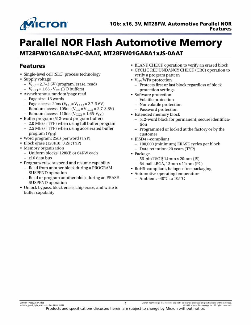
Parallel NOR Flash Automotive Memory MT28FW01GABA1xPC-0AAT, MT28FW01GABA1xJS-0AAT Features • Single-level cell (SLC) process technology • Supply voltage – V CC = 2.7–3.6V (program, erase, read) – V CCQ = 1.65 - V CC (I/O buffers) • Asynchronous random/page read – Page size: 16 words – Page access: 20ns (V CC = V CCQ = 2.7-3.6V) – Random access: 105ns (V CC = V CCQ = 2.7-3.6V) – Random access: 110ns (V CCQ = 1.65-V CC ) • Buffer program (512-word program buffer) – 2.0 MB/s (TYP) when using full buffer program – 2.5 MB/s (TYP) when using accelerated buffer program (V HH ) • Word program: 25us per word (TYP) • Block erase (128KB): 0.2s (TYP) • Memory organization – Uniform blocks: 128KB or 64KW each – x16 data bus • Program/erase suspend and resume capability – Read from another block during a PROGRAM SUSPEND operation – Read or program another block during an ERASE SUSPEND operation • Unlock bypass, block erase, chip erase, and write to buffer capability • BLANK CHECK operation to verify an erased block • CYCLIC REDUNDANCY CHECK (CRC) operation to verify a program pattern •V PP /WP# protection – Protects first or last block regardless of block protection settings • Software protection – Volatile protection – Nonvolatile protection – Password protection • Extended memory block – 512-word block for permanent, secure identifica- tion – Programmed or locked at the factory or by the customer • JESD47-compliant – 100,000 (minimum) ERASE cycles per block – Data retention: 20 years (TYP) • Package – 56-pin TSOP, 14mm x 20mm (JS) – 64-ball LBGA, 13mm x 11mm (PC) • RoHS-compliant, halogen-free packaging • Automotive operating temperature – Ambient: –40°C to 105°C 1Gb: x16, 3V, MT28FW, Automotive Parallel NOR Features CCMTD-1725822587-3365 mt28fw_genB_1gb_auto.pdf - Rev. H 05/18 EN 1 Micron Technology, Inc. reserves the right to change products or specifications without notice. © 2014 Micron Technology, Inc. All rights reserved. Products and specifications discussed herein are subject to change by Micron without notice.

Welcome message from author
This document is posted to help you gain knowledge. Please leave a comment to let me know what you think about it! Share it to your friends and learn new things together.
Transcript
Parallel NOR Flash Automotive MemoryMT28FW01GABA1xPC-0AAT, MT28FW01GABA1xJS-0AAT
Features• Single-level cell (SLC) process technology• Supply voltage
– VCC = 2.7–3.6V (program, erase, read)– VCCQ = 1.65 - VCC (I/O buffers)
• Asynchronous random/page read– Page size: 16 words– Page access: 20ns (VCC = VCCQ = 2.7-3.6V)– Random access: 105ns (VCC = VCCQ = 2.7-3.6V)– Random access: 110ns (VCCQ = 1.65-VCC)
• Buffer program (512-word program buffer)– 2.0 MB/s (TYP) when using full buffer program– 2.5 MB/s (TYP) when using accelerated buffer
program (VHH)• Word program: 25us per word (TYP)• Block erase (128KB): 0.2s (TYP)• Memory organization
– Uniform blocks: 128KB or 64KW each– x16 data bus
• Program/erase suspend and resume capability– Read from another block during a PROGRAM
SUSPEND operation– Read or program another block during an ERASE
SUSPEND operation• Unlock bypass, block erase, chip erase, and write to
buffer capability
• BLANK CHECK operation to verify an erased block• CYCLIC REDUNDANCY CHECK (CRC) operation to
verify a program pattern• VPP/WP# protection
– Protects first or last block regardless of blockprotection settings
• Software protection– Volatile protection– Nonvolatile protection– Password protection
• Extended memory block– 512-word block for permanent, secure identifica-
tion– Programmed or locked at the factory or by the
customer• JESD47-compliant
– 100,000 (minimum) ERASE cycles per block– Data retention: 20 years (TYP)
• Package– 56-pin TSOP, 14mm x 20mm (JS)– 64-ball LBGA, 13mm x 11mm (PC)
• RoHS-compliant, halogen-free packaging• Automotive operating temperature
– Ambient: –40°C to 105°C
1Gb: x16, 3V, MT28FW, Automotive Parallel NORFeatures
CCMTD-1725822587-3365mt28fw_genB_1gb_auto.pdf - Rev. H 05/18 EN 1 Micron Technology, Inc. reserves the right to change products or specifications without notice.
© 2014 Micron Technology, Inc. All rights reserved.
Products and specifications discussed herein are subject to change by Micron without notice.
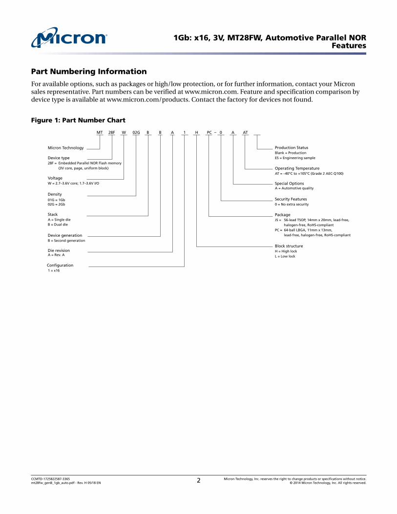
Part Numbering Information
For available options, such as packages or high/low protection, or for further information, contact your Micronsales representative. Part numbers can be verified at www.micron.com. Feature and specification comparison bydevice type is available at www.micron.com/products. Contact the factory for devices not found.
Figure 1: Part Number Chart
MT 28F W 02G B B A 1
Micron Technology
Device type28F = Embedded Parallel NOR Flash memory (3V core, page, uniform block)
VoltageW = 2.7–3.6V core; 1.7–3.6V I/O
Density01G = 1Gb02G = 2Gb
StackA = Single dieB = Dual die
A = Rev. A
Configuration1 = x16
H PC 0 A AT
Production StatusBlank = ProductionES = Engineering sample
Operating TemperatureAT = –40°C to +105°C (Grade 2 AEC-Q100)
Special OptionsA = Automotive quality
Security Features0 = No extra security
PackageJS = 56-lead TSOP, 14mm x 20mm, lead-free, halogen-free, RoHS-compliantPC = 64-ball LBGA, 11mm x 13mm, lead-free, halogen-free, RoHS-compliant
Block structure H = High lockL = Low lock
–
Device generationB = Second generation
Die revision
1Gb: x16, 3V, MT28FW, Automotive Parallel NORFeatures
CCMTD-1725822587-3365mt28fw_genB_1gb_auto.pdf - Rev. H 05/18 EN 2 Micron Technology, Inc. reserves the right to change products or specifications without notice.
© 2014 Micron Technology, Inc. All rights reserved.
ContentsImportant Notes and Warnings ......................................................................................................................... 7General Description ......................................................................................................................................... 8
Automatic Power Savings Feature .................................................................................................................. 8Signal Assignments ......................................................................................................................................... 10Signal Descriptions ......................................................................................................................................... 12Memory Organization .................................................................................................................................... 14
Memory Configuration ............................................................................................................................... 14Memory Map ............................................................................................................................................. 14
Bus Operations ............................................................................................................................................... 15Read .......................................................................................................................................................... 15Write .......................................................................................................................................................... 15Standby ..................................................................................................................................................... 15Output Disable ........................................................................................................................................... 16Reset .......................................................................................................................................................... 16
Registers ........................................................................................................................................................ 17Data Polling Register .................................................................................................................................. 17Read Status Register ................................................................................................................................... 22Clear Status Register ................................................................................................................................... 23Lock Register .............................................................................................................................................. 24
Standard Command Definitions – Address-Data Cycles .................................................................................... 26READ and AUTO SELECT Operations .............................................................................................................. 28
READ/RESET Command ............................................................................................................................ 28READ CFI Command .................................................................................................................................. 28AUTO SELECT Command ........................................................................................................................... 28Read Electronic Signature ........................................................................................................................... 29
Cyclic Redundancy Check Operation ............................................................................................................... 30CYCLIC REDUNDANCY CHECK Command ................................................................................................. 30Cyclic Redundancy Check Operation Command Sequence .......................................................................... 30
Bypass Operations .......................................................................................................................................... 33UNLOCK BYPASS Command ...................................................................................................................... 33UNLOCK BYPASS RESET Command ............................................................................................................ 33
Program Operations ....................................................................................................................................... 34PROGRAM Command ................................................................................................................................ 34UNLOCK BYPASS PROGRAM Command ..................................................................................................... 34WRITE TO BUFFER PROGRAM Command .................................................................................................. 34UNLOCK BYPASS WRITE TO BUFFER PROGRAM Command ....................................................................... 37WRITE TO BUFFER PROGRAM CONFIRM Command .................................................................................. 37BUFFERED PROGRAM ABORT AND RESET Command ................................................................................ 37PROGRAM SUSPEND Command ................................................................................................................ 37PROGRAM RESUME Command .................................................................................................................. 38ACCELERATED BUFFERED PROGRAM Operations ...................................................................................... 38
Erase Operations ............................................................................................................................................ 39CHIP ERASE Command .............................................................................................................................. 39UNLOCK BYPASS CHIP ERASE Command ................................................................................................... 39BLOCK ERASE Command ........................................................................................................................... 39UNLOCK BYPASS BLOCK ERASE Command ................................................................................................ 40ERASE SUSPEND Command ....................................................................................................................... 40ERASE RESUME Command ........................................................................................................................ 41
ACCELERATED CHIP ERASE Operations ......................................................................................................... 41BLANK CHECK Operation .............................................................................................................................. 41
1Gb: x16, 3V, MT28FW, Automotive Parallel NORFeatures
CCMTD-1725822587-3365mt28fw_genB_1gb_auto.pdf - Rev. H 05/18 EN 3 Micron Technology, Inc. reserves the right to change products or specifications without notice.
© 2014 Micron Technology, Inc. All rights reserved.
Device Protection ........................................................................................................................................... 43Hardware Protection .................................................................................................................................. 43Software Protection .................................................................................................................................... 43Volatile Protection Mode ............................................................................................................................. 44Nonvolatile Protection Mode ...................................................................................................................... 44Password Protection Mode .......................................................................................................................... 44
Block Protection Command Definitions – Address-Data Cycles ........................................................................ 47Protection Operations .................................................................................................................................... 50
LOCK REGISTER Commands ...................................................................................................................... 50PASSWORD PROTECTION Commands ....................................................................................................... 50NONVOLATILE PROTECTION Commands .................................................................................................. 50NONVOLATILE PROTECTION BIT LOCK BIT Commands ............................................................................ 51VOLATILE PROTECTION Commands .......................................................................................................... 52EXTENDED MEMORY BLOCK Commands .................................................................................................. 52EXIT PROTECTION Command .................................................................................................................... 53
Common Flash Interface ................................................................................................................................ 54Power-Up and Reset Characteristics ................................................................................................................ 59Absolute Ratings and Operating Conditions ..................................................................................................... 61DC Characteristics .......................................................................................................................................... 63Read AC Characteristics .................................................................................................................................. 65Write AC Characteristics ................................................................................................................................. 67Data Polling/Toggle AC Characteristics ............................................................................................................ 72Program/Erase Characteristics ........................................................................................................................ 74Package Dimensions ....................................................................................................................................... 75Revision History ............................................................................................................................................. 77
Rev. H –05/18 ............................................................................................................................................. 77Rev. G – 11/16 ............................................................................................................................................. 77Rev. F – 6/16 ............................................................................................................................................... 77Rev. E – 9/15 ............................................................................................................................................... 77Rev. D – 01/15 ............................................................................................................................................. 77Rev. C – 12/14 ............................................................................................................................................. 77Rev. B – 07/14 ............................................................................................................................................. 77Rev. A – 05/14 ............................................................................................................................................. 77
1Gb: x16, 3V, MT28FW, Automotive Parallel NORFeatures
CCMTD-1725822587-3365mt28fw_genB_1gb_auto.pdf - Rev. H 05/18 EN 4 Micron Technology, Inc. reserves the right to change products or specifications without notice.
© 2014 Micron Technology, Inc. All rights reserved.
List of FiguresFigure 1: Part Number Chart ............................................................................................................................ 2Figure 2: Logic Diagram ................................................................................................................................... 9Figure 3: 56-Pin TSOP (Top View) .................................................................................................................. 10Figure 4: 64-Ball LBGA (Top View – Balls Down) ............................................................................................. 11Figure 5: Data Polling Flowchart .................................................................................................................... 19Figure 6: Toggle Bit Flowchart ........................................................................................................................ 20Figure 7: Data Polling/Toggle Bit Flowchart .................................................................................................... 21Figure 8: Lock Register Program Flowchart ..................................................................................................... 25Figure 9: Boundary Condition of Program Buffer Size ..................................................................................... 35Figure 10: WRITE TO BUFFER PROGRAM Flowchart ...................................................................................... 36Figure 11: Software Protection Scheme .......................................................................................................... 45Figure 12: Set/Clear Nonvolatile Protection Bit Algorithm Flowchart ............................................................... 51Figure 13: Power-Up Timing .......................................................................................................................... 59Figure 14: Reset AC Timing – No PROGRAM/ERASE Operation in Progress ...................................................... 60Figure 15: Reset AC Timing During PROGRAM/ERASE Operation .................................................................... 60Figure 16: AC Measurement Load Circuit ....................................................................................................... 62Figure 17: AC Measurement I/O Waveform ..................................................................................................... 62Figure 18: Random Read AC Timing ............................................................................................................... 66Figure 19: Page Read AC Timing ..................................................................................................................... 66Figure 20: WE#-Controlled Program AC Timing .............................................................................................. 68Figure 21: CE#-Controlled Program AC Timing ............................................................................................... 70Figure 22: Chip/Block Erase AC Timing .......................................................................................................... 71Figure 23: Accelerated Program AC Timing ..................................................................................................... 71Figure 24: Data Polling AC Timing .................................................................................................................. 72Figure 25: Toggle/Alternative Toggle Bit Polling AC Timing .............................................................................. 73Figure 26: 56-Pin TSOP – 14mm x 20mm (Package Code: JS) ............................................................................ 75Figure 27: 64-Ball LBGA – 11mm x 13mm (Package Code: PC) ......................................................................... 76
1Gb: x16, 3V, MT28FW, Automotive Parallel NORFeatures
CCMTD-1725822587-3365mt28fw_genB_1gb_auto.pdf - Rev. H 05/18 EN 5 Micron Technology, Inc. reserves the right to change products or specifications without notice.
© 2014 Micron Technology, Inc. All rights reserved.
List of TablesTable 1: Signal Descriptions ........................................................................................................................... 12Table 2: Blocks[1023:0] .................................................................................................................................. 14Table 3: Bus Operations ................................................................................................................................. 15Table 4: Data Polling Register Bit Definitions .................................................................................................. 17Table 5: Operations and Corresponding Bit Settings ........................................................................................ 18Table 6: Status Register Definitions ................................................................................................................ 22Table 7: Lock Register Bit Definitions ............................................................................................................. 24Table 8: Standard Command Definitions – Address-Data Cycles ...................................................................... 26Table 9: Block Protection ............................................................................................................................... 29Table 10: Read Electronic Signature – 1Gb ...................................................................................................... 29Table 11: Command Sequence – Range of Blocks ............................................................................................ 30Table 12: Command Sequence – Entire Chip .................................................................................................. 32Table 13: ACCELERATED PROGRAM Requirements and Recommendations .................................................... 38Table 14: ACCELERATED CHIP ERASE Requirements and Recommendations ................................................. 41Table 15: VPP/WP# Functions ......................................................................................................................... 43Table 16: Block Protection Status ................................................................................................................... 46Table 17: Block Protection Command Definitions – Address-Data Cycles ......................................................... 47Table 18: Extended Memory Block Address and Data ...................................................................................... 52Table 19: Query Structure Overview ............................................................................................................... 54Table 20: CFI Query Identification String ........................................................................................................ 54Table 21: CFI Query System Interface Information .......................................................................................... 55Table 22: Device Geometry Definition ............................................................................................................ 55Table 23: Primary Algorithm-Specific Extended Query Table ........................................................................... 56Table 24: Power-Up Specifications ................................................................................................................. 59Table 25: Reset AC Specifications ................................................................................................................... 60Table 26: Absolute Maximum/Minimum Ratings ............................................................................................ 61Table 27: Operating Conditions ...................................................................................................................... 61Table 28: Input/Output Capacitance .............................................................................................................. 62Table 29: DC Current Characteristics .............................................................................................................. 63Table 30: DC Voltage Characteristics .............................................................................................................. 64Table 31: Read AC Characteristics – VCC = VCCQ = 2.7–3.6V ............................................................................... 65Table 32: Read AC Characteristics – VCCQ = 1.65V–VCC ..................................................................................... 65Table 33: WE#-Controlled Write AC Characteristics ......................................................................................... 67Table 34: CE#-Controlled Write AC Characteristics ......................................................................................... 69Table 35: Data Polling/Toggle AC Characteristics ............................................................................................ 72Table 36: Program/Erase Characteristics ........................................................................................................ 74
1Gb: x16, 3V, MT28FW, Automotive Parallel NORFeatures
CCMTD-1725822587-3365mt28fw_genB_1gb_auto.pdf - Rev. H 05/18 EN 6 Micron Technology, Inc. reserves the right to change products or specifications without notice.
© 2014 Micron Technology, Inc. All rights reserved.
Important Notes and WarningsMicron Technology, Inc. ("Micron") reserves the right to make changes to information published in this document,including without limitation specifications and product descriptions. This document supersedes and replaces allinformation supplied prior to the publication hereof. You may not rely on any information set forth in this docu-ment if you obtain the product described herein from any unauthorized distributor or other source not authorizedby Micron.
Automotive Applications. Products are not designed or intended for use in automotive applications unless specifi-cally designated by Micron as automotive-grade by their respective data sheets. Distributor and customer/distrib-utor shall assume the sole risk and liability for and shall indemnify and hold Micron harmless against all claims,costs, damages, and expenses and reasonable attorneys' fees arising out of, directly or indirectly, any claim ofproduct liability, personal injury, death, or property damage resulting directly or indirectly from any use of non-automotive-grade products in automotive applications. Customer/distributor shall ensure that the terms and con-ditions of sale between customer/distributor and any customer of distributor/customer (1) state that Micronproducts are not designed or intended for use in automotive applications unless specifically designated by Micronas automotive-grade by their respective data sheets and (2) require such customer of distributor/customer to in-demnify and hold Micron harmless against all claims, costs, damages, and expenses and reasonable attorneys'fees arising out of, directly or indirectly, any claim of product liability, personal injury, death, or property damageresulting from any use of non-automotive-grade products in automotive applications.
Critical Applications. Products are not authorized for use in applications in which failure of the Micron compo-nent could result, directly or indirectly in death, personal injury, or severe property or environmental damage("Critical Applications"). Customer must protect against death, personal injury, and severe property and environ-mental damage by incorporating safety design measures into customer's applications to ensure that failure of theMicron component will not result in such harms. Should customer or distributor purchase, use, or sell any Microncomponent for any critical application, customer and distributor shall indemnify and hold harmless Micron andits subsidiaries, subcontractors, and affiliates and the directors, officers, and employees of each against all claims,costs, damages, and expenses and reasonable attorneys' fees arising out of, directly or indirectly, any claim ofproduct liability, personal injury, or death arising in any way out of such critical application, whether or not Mi-cron or its subsidiaries, subcontractors, or affiliates were negligent in the design, manufacture, or warning of theMicron product.
Customer Responsibility. Customers are responsible for the design, manufacture, and operation of their systems,applications, and products using Micron products. ALL SEMICONDUCTOR PRODUCTS HAVE INHERENT FAIL-URE RATES AND LIMITED USEFUL LIVES. IT IS THE CUSTOMER'S SOLE RESPONSIBILITY TO DETERMINEWHETHER THE MICRON PRODUCT IS SUITABLE AND FIT FOR THE CUSTOMER'S SYSTEM, APPLICATION, ORPRODUCT. Customers must ensure that adequate design, manufacturing, and operating safeguards are includedin customer's applications and products to eliminate the risk that personal injury, death, or severe property or en-vironmental damages will result from failure of any semiconductor component.
Limited Warranty. In no event shall Micron be liable for any indirect, incidental, punitive, special or consequentialdamages (including without limitation lost profits, lost savings, business interruption, costs related to the removalor replacement of any products or rework charges) whether or not such damages are based on tort, warranty,breach of contract or other legal theory, unless explicitly stated in a written agreement executed by Micron's dulyauthorized representative.
1Gb: x16, 3V, MT28FW, Automotive Parallel NORImportant Notes and Warnings
CCMTD-1725822587-3365mt28fw_genB_1gb_auto.pdf - Rev. H 05/18 EN 7 Micron Technology, Inc. reserves the right to change products or specifications without notice.
© 2014 Micron Technology, Inc. All rights reserved.
General DescriptionThe device is an asynchronous, uniform block, parallel NOR Flash memory device.READ, ERASE, and PROGRAM operations are performed using a single low-voltage sup-ply. Upon power-up, the device defaults to read array mode.
The main memory array is divided into uniform blocks that can be erased independent-ly so that valid data can be preserved while old data is purged. PROGRAM and ERASEcommands are written to the command interface of the memory. An on-chip program/erase controller simplifies the process of programming or erasing the memory by takingcare of all special operations required to update the memory contents. The end of aPROGRAM or ERASE operation can be detected and any error condition can be identi-fied. The command set required to control the device is consistent with JEDEC stand-ards.
CE#, OE#, and WE# control the bus operation of the device and enable a simple con-nection to most microprocessors, often without additional logic.
The device supports asynchronous random read and page read from all blocks of thearray. It also features an internal program buffer that improves throughput by program-ming 512 words via one command sequence. A 512-word extended memory block over-laps addresses with array block 0. Users can program this additional space and thenprotect it to permanently secure the contents. The device also features different levels ofhardware and software protection to secure blocks from unwanted modification.
Automatic Power Savings Feature
The automatic power savings feature provides low power operation during reads.
After data is read from the memory array and the address lines are quiescent, the auto-matic power savings feature reduces device current to a low value of ICCAPS.
During automatic power savings mode, average current is measured over 5ms time in-terval 5μs after the following events happen:
• No internal read, program or erase activity occurring• RST# is deasserted and CE# is asserted• All other signals are quiescent and at VSS or VCCQ
1Gb: x16, 3V, MT28FW, Automotive Parallel NORGeneral Description
CCMTD-1725822587-3365mt28fw_genB_1gb_auto.pdf - Rev. H 05/18 EN 8 Micron Technology, Inc. reserves the right to change products or specifications without notice.
© 2014 Micron Technology, Inc. All rights reserved.
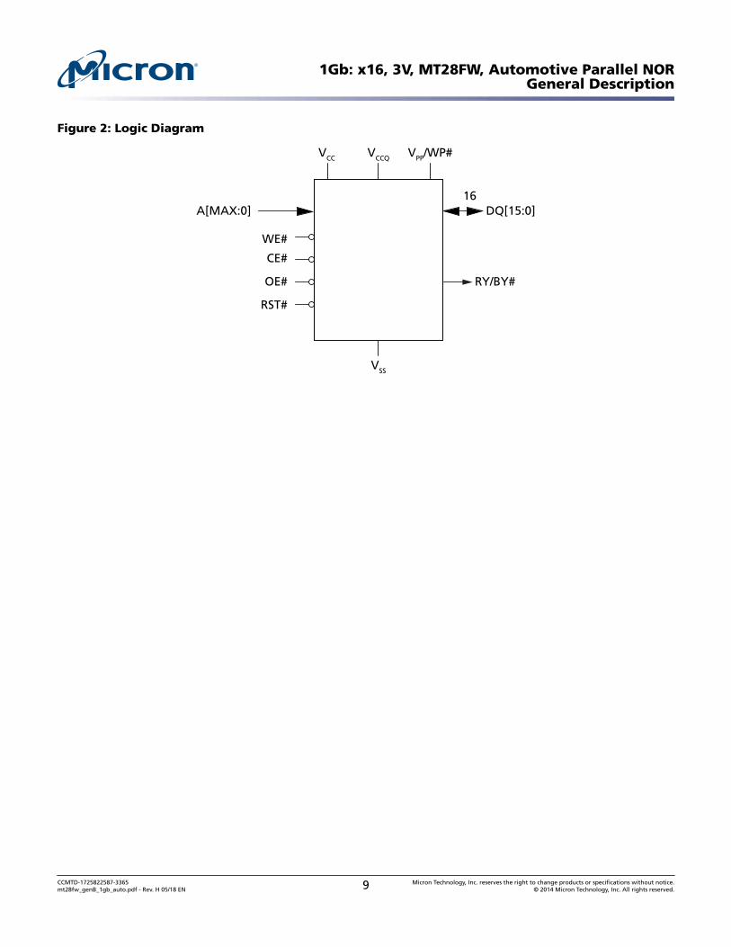
Figure 2: Logic Diagram
VCC VCCQ
A[MAX:0]
WE#
VPP/WP#
DQ[15:0]
VSS
16
CE#
OE#
RST#
RY/BY#
1Gb: x16, 3V, MT28FW, Automotive Parallel NORGeneral Description
CCMTD-1725822587-3365mt28fw_genB_1gb_auto.pdf - Rev. H 05/18 EN 9 Micron Technology, Inc. reserves the right to change products or specifications without notice.
© 2014 Micron Technology, Inc. All rights reserved.
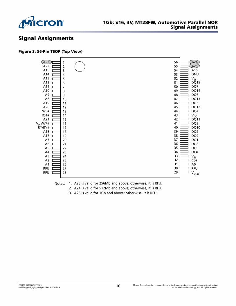
Signal Assignments
Figure 3: 56-Pin TSOP (Top View)
12345678910111213141516171819202122232425262728
56555453525150494847464544434241403938373635343332313029
A23A22A15A14A13A12A11A10A9A8
A19A20
WE#RST#A21
VPP/WP#RY/BY#
A18A17A7A6A5A4A3A2A1
RFURFU
A24A25A16DNUVSSDQ15DQ7DQ14DQ6DQ13DQ5DQ12DQ4VCCDQ11DQ3DQ10DQ2DQ9DQ1DQ8DQ0OE#VSSCE#A0RFUVCCQ
Notes: 1. A23 is valid for 256Mb and above; otherwise, it is RFU.2. A24 is valid for 512Mb and above; otherwise, it is RFU.3. A25 is valid for 1Gb and above; otherwise, it is RFU.
1Gb: x16, 3V, MT28FW, Automotive Parallel NORSignal Assignments
CCMTD-1725822587-3365mt28fw_genB_1gb_auto.pdf - Rev. H 05/18 EN 10 Micron Technology, Inc. reserves the right to change products or specifications without notice.
© 2014 Micron Technology, Inc. All rights reserved.
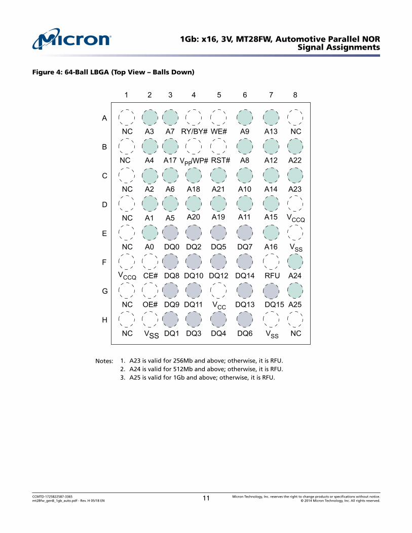
Figure 4: 64-Ball LBGA (Top View – Balls Down)
A
B
C
D
E
F
G
H
1
NC
NC
NC
NC
NC
NC
VCCQ
NC
2
A3
A4
A2
A1
A0
CE#
OE#
VSS
3
A7
A17
A6
A5
DQ0
DQ8
DQ9
DQ1
4
RY/BY#
A18
A20
DQ2
DQ10
DQ11
DQ3
5
WE#
VPP/WP# RST#
A21
A19
DQ5
DQ12
VCC
DQ4
6
A9
A8
A10
A11
DQ7
DQ14
DQ13
DQ6
7
A13
A12
A14
A15
A16
RFU
DQ15
VSS
8
NC
A22
A23
VCCQ
VSS
A24
A25
NC
Notes: 1. A23 is valid for 256Mb and above; otherwise, it is RFU.2. A24 is valid for 512Mb and above; otherwise, it is RFU.3. A25 is valid for 1Gb and above; otherwise, it is RFU.
1Gb: x16, 3V, MT28FW, Automotive Parallel NORSignal Assignments
CCMTD-1725822587-3365mt28fw_genB_1gb_auto.pdf - Rev. H 05/18 EN 11 Micron Technology, Inc. reserves the right to change products or specifications without notice.
© 2014 Micron Technology, Inc. All rights reserved.
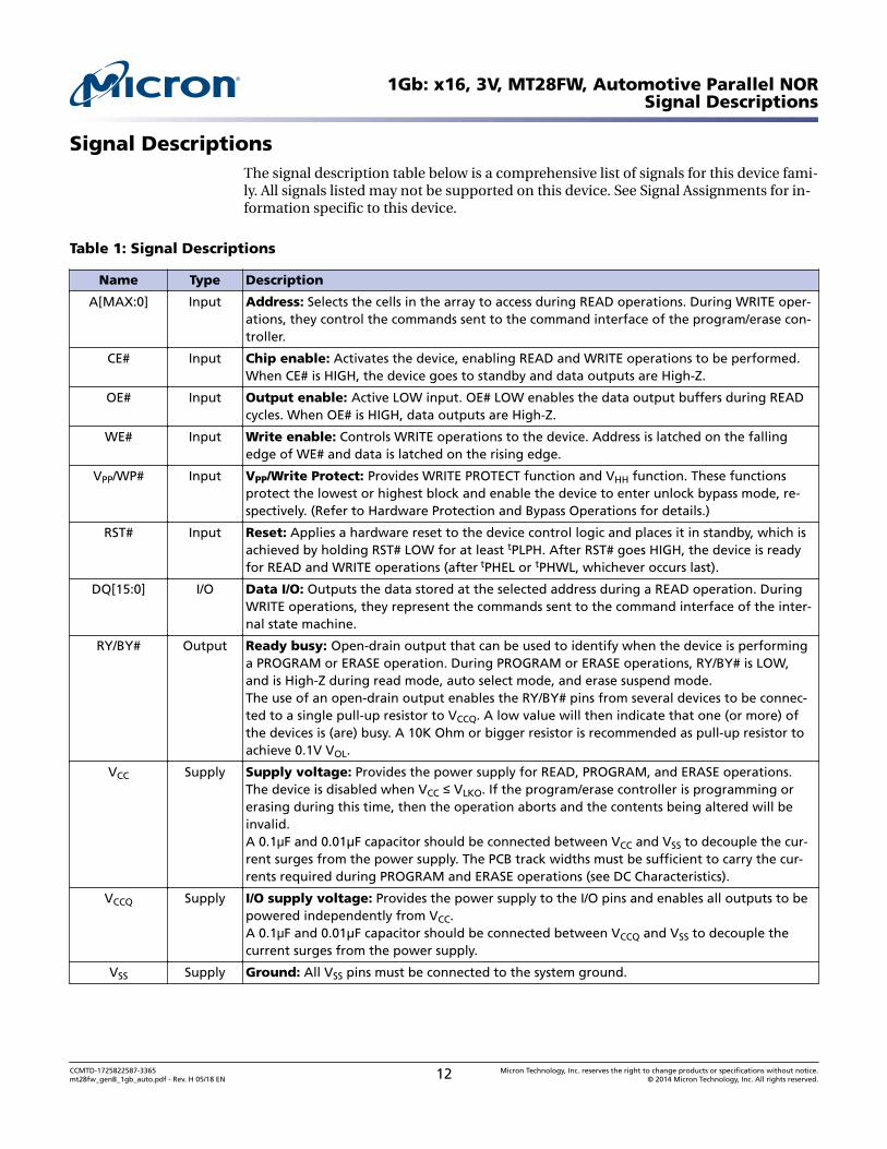
Signal DescriptionsThe signal description table below is a comprehensive list of signals for this device fami-ly. All signals listed may not be supported on this device. See Signal Assignments for in-formation specific to this device.
Table 1: Signal Descriptions
Name Type Description
A[MAX:0] Input Address: Selects the cells in the array to access during READ operations. During WRITE oper-ations, they control the commands sent to the command interface of the program/erase con-troller.
CE# Input Chip enable: Activates the device, enabling READ and WRITE operations to be performed.When CE# is HIGH, the device goes to standby and data outputs are High-Z.
OE# Input Output enable: Active LOW input. OE# LOW enables the data output buffers during READcycles. When OE# is HIGH, data outputs are High-Z.
WE# Input Write enable: Controls WRITE operations to the device. Address is latched on the fallingedge of WE# and data is latched on the rising edge.
VPP/WP# Input VPP/Write Protect: Provides WRITE PROTECT function and VHH function. These functionsprotect the lowest or highest block and enable the device to enter unlock bypass mode, re-spectively. (Refer to Hardware Protection and Bypass Operations for details.)
RST# Input Reset: Applies a hardware reset to the device control logic and places it in standby, which isachieved by holding RST# LOW for at least tPLPH. After RST# goes HIGH, the device is readyfor READ and WRITE operations (after tPHEL or tPHWL, whichever occurs last).
DQ[15:0] I/O Data I/O: Outputs the data stored at the selected address during a READ operation. DuringWRITE operations, they represent the commands sent to the command interface of the inter-nal state machine.
RY/BY# Output Ready busy: Open-drain output that can be used to identify when the device is performinga PROGRAM or ERASE operation. During PROGRAM or ERASE operations, RY/BY# is LOW,and is High-Z during read mode, auto select mode, and erase suspend mode.The use of an open-drain output enables the RY/BY# pins from several devices to be connec-ted to a single pull-up resistor to VCCQ. A low value will then indicate that one (or more) ofthe devices is (are) busy. A 10K Ohm or bigger resistor is recommended as pull-up resistor toachieve 0.1V VOL.
VCC Supply Supply voltage: Provides the power supply for READ, PROGRAM, and ERASE operations.The device is disabled when VCC ≤ VLKO. If the program/erase controller is programming orerasing during this time, then the operation aborts and the contents being altered will beinvalid.A 0.1μF and 0.01µF capacitor should be connected between VCC and VSS to decouple the cur-rent surges from the power supply. The PCB track widths must be sufficient to carry the cur-rents required during PROGRAM and ERASE operations (see DC Characteristics).
VCCQ Supply I/O supply voltage: Provides the power supply to the I/O pins and enables all outputs to bepowered independently from VCC.A 0.1μF and 0.01µF capacitor should be connected between VCCQ and VSS to decouple thecurrent surges from the power supply.
VSS Supply Ground: All VSS pins must be connected to the system ground.
1Gb: x16, 3V, MT28FW, Automotive Parallel NORSignal Descriptions
CCMTD-1725822587-3365mt28fw_genB_1gb_auto.pdf - Rev. H 05/18 EN 12 Micron Technology, Inc. reserves the right to change products or specifications without notice.
© 2014 Micron Technology, Inc. All rights reserved.
Table 1: Signal Descriptions (Continued)
Name Type Description
RFU — Reserved for future use: Reserved by Micron for future device functionality and enhance-ment. Recommend that these be left floating. May be connected internally, but external con-nections will not affect operation.
DNU — Do not use: Do not connect to any other signal, or power supply; must be left floating.
NC — No connect: No internal connection; can be driven or floated.
1Gb: x16, 3V, MT28FW, Automotive Parallel NORSignal Descriptions
CCMTD-1725822587-3365mt28fw_genB_1gb_auto.pdf - Rev. H 05/18 EN 13 Micron Technology, Inc. reserves the right to change products or specifications without notice.
© 2014 Micron Technology, Inc. All rights reserved.
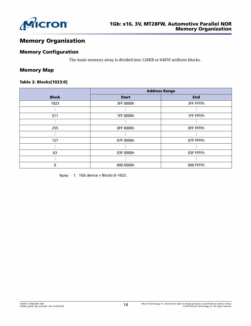
Memory Organization
Memory Configuration
The main memory array is divided into 128KB or 64KW uniform blocks.
Memory Map
Table 2: Blocks[1023:0]
Block
Address Range
Start End
1023 3FF 0000h 3FF FFFFh
⋮ ⋮ ⋮511 1FF 0000h 1FF FFFFh
⋮ ⋮ ⋮255 0FF 0000h 0FF FFFFh
⋮ ⋮ ⋮127 07F 0000h 07F FFFFh
⋮ ⋮ ⋮63 03F 0000h 03F FFFFh
⋮ ⋮ ⋮0 000 0000h 000 FFFFh
Note: 1. 1Gb device = Blocks 0–1023.
1Gb: x16, 3V, MT28FW, Automotive Parallel NORMemory Organization
CCMTD-1725822587-3365mt28fw_genB_1gb_auto.pdf - Rev. H 05/18 EN 14 Micron Technology, Inc. reserves the right to change products or specifications without notice.
© 2014 Micron Technology, Inc. All rights reserved.
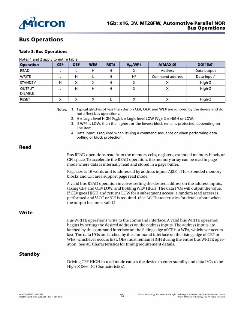
Bus Operations
Table 3: Bus Operations
Notes 1 and 2 apply to entire tableOperation CE# OE# WE# RST# VPP/WP# A[MAX:0] DQ[15:0]
READ L L H H X Address Data output
WRITE L H L H H3 Command address Data input4
STANDBY H X X H X X High-Z
OUTPUTDISABLE
L H H H X X High-Z
RESET X X X L X X High-Z
Notes: 1. Typical glitches of less than 3ns on CE#, OE#, and WE# are ignored by the device and donot affect bus operations.
2. H = Logic level HIGH (VIH); L = Logic level LOW (VIL); X = HIGH or LOW.3. If WP# is LOW, then the highest or the lowest block remains protected, depending on
line item.4. Data input is required when issuing a command sequence or when performing data
polling or block protection.
Read
Bus READ operations read from the memory cells, registers, extended memory block, orCFI space. To accelerate the READ operation, the memory array can be read in pagemode where data is internally read and stored in a page buffer.
Page size is 16 words and is addressed by address inputs A[3:0]. The extended memoryblocks and CFI area support page read mode.
A valid bus READ operation involves setting the desired address on the address inputs,taking CE# and OE# LOW, and holding WE# HIGH. The data I/Os will output the value.If CE# goes HIGH and returns LOW for a subsequent access, a random read access isperformed and tACC or tCE is required. (See AC Characteristics for details about whenthe output becomes valid.)
Write
Bus WRITE operations write to the command interface. A valid bus WRITE operationbegins by setting the desired address on the address inputs. The address inputs arelatched by the command interface on the falling edge of CE# or WE#, whichever occurslast. The data I/Os are latched by the command interface on the rising edge of CE# orWE#, whichever occurs first. OE# must remain HIGH during the entire bus WRITE oper-ation (See AC Characteristics for timing requirement details).
Standby
Driving CE# HIGH in read mode causes the device to enter standby and data I/Os to beHigh-Z (See DC Characteristics).
1Gb: x16, 3V, MT28FW, Automotive Parallel NORBus Operations
CCMTD-1725822587-3365mt28fw_genB_1gb_auto.pdf - Rev. H 05/18 EN 15 Micron Technology, Inc. reserves the right to change products or specifications without notice.
© 2014 Micron Technology, Inc. All rights reserved.
During PROGRAM or ERASE operations, the device will continue to use the program/erase supply current (ICC3) until the operation completes. The device cannot be placedinto standby mode during a PROGRAM/ERASE operation.
Output Disable
Data I/Os are High-Z when OE# is HIGH.
Reset
During reset mode the device is deselected and the outputs are High-Z. The device is inreset mode when RST# is LOW. The power consumption is reduced to the standby level,independently from CE#, OE#, or WE# inputs.
When RST# is HIGH, a time of tPHEL is required before a READ operation can accessthe device, and a delay of tPHWL is required before a write sequence can be initiated.After this wake-up interval, normal operation is restored, the device defaults to read ar-ray mode, and the data polling register is reset.
If RST# is driven LOW during a PROGRAM/ERASE operation or any other operation thatrequires writing to the device, the operation will abort within tPLRH, and memory con-tents at the aborted block or address are no longer valid.
1Gb: x16, 3V, MT28FW, Automotive Parallel NORBus Operations
CCMTD-1725822587-3365mt28fw_genB_1gb_auto.pdf - Rev. H 05/18 EN 16 Micron Technology, Inc. reserves the right to change products or specifications without notice.
© 2014 Micron Technology, Inc. All rights reserved.
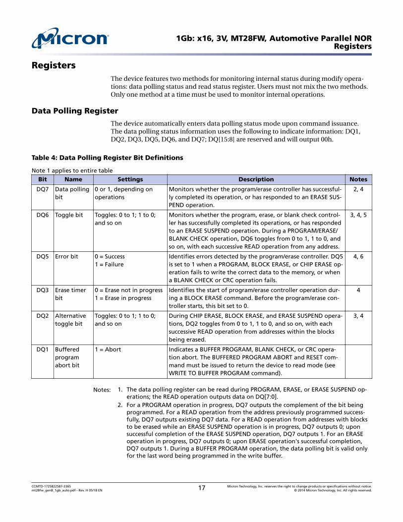
RegistersThe device features two methods for monitoring internal status during modify opera-tions: data polling status and read status register. Users must not mix the two methods.Only one method at a time must be used to monitor internal operations.
Data Polling Register
The device automatically enters data polling status mode upon command issuance.The data polling status information uses the following to indicate information: DQ1,DQ2, DQ3, DQ5, DQ6, and DQ7; DQ[15:8] are reserved and will output 00h.
Table 4: Data Polling Register Bit Definitions
Note 1 applies to entire tableBit Name Settings Description Notes
DQ7 Data pollingbit
0 or 1, depending onoperations
Monitors whether the program/erase controller has successful-ly completed its operation, or has responded to an ERASE SUS-PEND operation.
2, 4
DQ6 Toggle bit Toggles: 0 to 1; 1 to 0;and so on
Monitors whether the program, erase, or blank check control-ler has successfully completed its operations, or has respondedto an ERASE SUSPEND operation. During a PROGRAM/ERASE/BLANK CHECK operation, DQ6 toggles from 0 to 1, 1 to 0, andso on, with each successive READ operation from any address.
3, 4, 5
DQ5 Error bit 0 = Success1 = Failure
Identifies errors detected by the program/erase controller. DQ5is set to 1 when a PROGRAM, BLOCK ERASE, or CHIP ERASE op-eration fails to write the correct data to the memory, or whena BLANK CHECK or CRC operation fails.
4, 6
DQ3 Erase timerbit
0 = Erase not in progress1 = Erase in progress
Identifies the start of program/erase controller operation dur-ing a BLOCK ERASE command. Before the program/erase con-troller starts, this bit set to 0.
4
DQ2 Alternativetoggle bit
Toggles: 0 to 1; 1 to 0;and so on
During CHIP ERASE, BLOCK ERASE, and ERASE SUSPEND opera-tions, DQ2 toggles from 0 to 1, 1 to 0, and so on, with eachsuccessive READ operation from addresses within the blocksbeing erased.
3, 4
DQ1 Bufferedprogramabort bit
1 = Abort Indicates a BUFFER PROGRAM, BLANK CHECK, or CRC opera-tion abort. The BUFFERED PROGRAM ABORT and RESET com-mand must be issued to return the device to read mode (seeWRITE TO BUFFER PROGRAM command).
Notes: 1. The data polling register can be read during PROGRAM, ERASE, or ERASE SUSPEND op-erations; the READ operation outputs data on DQ[7:0].
2. For a PROGRAM operation in progress, DQ7 outputs the complement of the bit beingprogrammed. For a READ operation from the address previously programmed success-fully, DQ7 outputs existing DQ7 data. For a READ operation from addresses with blocksto be erased while an ERASE SUSPEND operation is in progress, DQ7 outputs 0; uponsuccessful completion of the ERASE SUSPEND operation, DQ7 outputs 1. For an ERASEoperation in progress, DQ7 outputs 0; upon ERASE operation's successful completion,DQ7 outputs 1. During a BUFFER PROGRAM operation, the data polling bit is valid onlyfor the last word being programmed in the write buffer.
1Gb: x16, 3V, MT28FW, Automotive Parallel NORRegisters
CCMTD-1725822587-3365mt28fw_genB_1gb_auto.pdf - Rev. H 05/18 EN 17 Micron Technology, Inc. reserves the right to change products or specifications without notice.
© 2014 Micron Technology, Inc. All rights reserved.
3. After successful completion of a PROGRAM, ERASE, or BLANK CHECK operation, the de-vice returns to read mode.
4. During erase suspend mode, READ operations to addresses within blocks not beingerased output memory array data as if in read mode. A protected block is treated thesame as a block not being erased. See the Toggle Flowchart for more information.
5. During erase suspend mode, DQ6 toggles when addressing a cell within a block beingerased. The toggling stops when the program/erase controller has suspended the ERASEoperation. See the Toggle Flowchart for more information.
6. When DQ5 is set to 1, a READ/RESET (F0h) command must be issued before any subse-quent command.
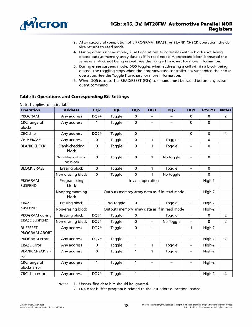
Table 5: Operations and Corresponding Bit Settings
Note 1 applies to entire tableOperation Address DQ7 DQ6 DQ5 DQ3 DQ2 DQ1 RY/BY# Notes
PROGRAM Any address DQ7# Toggle 0 – – 0 0 2
CRC range ofblocks
Any address 1 Toggle 0 – – 0 0
CRC chip Any address DQ7# Toggle 0 – – 0 0 4
CHIP ERASE Any address 0 Toggle 0 1 Toggle – 0
BLANK CHECK Blank-checkingblock
0 Toggle 0 1 Toggle – 0
Non-blank-check-ing block
0 Toggle 0 1 No toggle – 0
BLOCK ERASE Erasing block 0 Toggle 0 1 Toggle – 0
Non-erasing block 0 Toggle 0 1 No toggle – 0
PROGRAMSUSPEND
Programmingblock
Invalid operation High-Z
Nonprogrammingblock
Outputs memory array data as if in read mode High-Z
ERASESUSPEND
Erasing block 1 No Toggle 0 – Toggle – High-Z
Non-erasing block Outputs memory array data as if in read mode High-Z
PROGRAM duringERASE SUSPEND
Erasing block DQ7# Toggle 0 – Toggle – 0 2
Non-erasing block DQ7# Toggle 0 – No Toggle – 0 2
BUFFEREDPROGRAM ABORT
Any address DQ7# Toggle 0 – – 1 High-Z
PROGRAM Error Any address DQ7# Toggle 1 – – – High-Z 2
ERASE Error Any address 0 Toggle 1 1 Toggle – High-Z
BLANK CHECK Er-ror
Any address 0 Toggle 1 1 Toggle – High-Z
CRC range ofblocks error
Any address 1 Toggle 1 – – – High-Z
CRC chip error Any address DQ7# Toggle 1 – – – High-Z 4
Notes: 1. Unspecified data bits should be ignored.2. DQ7# for buffer program is related to the last address location loaded.
1Gb: x16, 3V, MT28FW, Automotive Parallel NORRegisters
CCMTD-1725822587-3365mt28fw_genB_1gb_auto.pdf - Rev. H 05/18 EN 18 Micron Technology, Inc. reserves the right to change products or specifications without notice.
© 2014 Micron Technology, Inc. All rights reserved.
3. DQ7# is the reverse DQ7 of the last word or byte loaded before CRC chip confirm com-mand cycle.
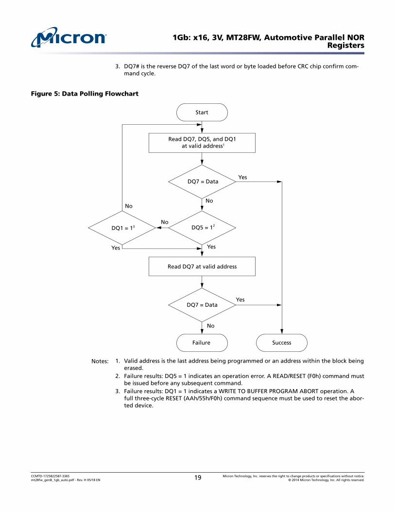
Figure 5: Data Polling Flowchart
Start
DQ7 = Data
DQ5 = 1DQ1 = 1
DQ7 = Data
No
No
No
No
Yes
Yes
Yes
Yes
Read DQ7, DQ5, and DQ1at valid address1
Read DQ7 at valid address
SuccessFailure
3 2
Notes: 1. Valid address is the last address being programmed or an address within the block beingerased.
2. Failure results: DQ5 = 1 indicates an operation error. A READ/RESET (F0h) command mustbe issued before any subsequent command.
3. Failure results: DQ1 = 1 indicates a WRITE TO BUFFER PROGRAM ABORT operation. Afull three-cycle RESET (AAh/55h/F0h) command sequence must be used to reset the abor-ted device.
1Gb: x16, 3V, MT28FW, Automotive Parallel NORRegisters
CCMTD-1725822587-3365mt28fw_genB_1gb_auto.pdf - Rev. H 05/18 EN 19 Micron Technology, Inc. reserves the right to change products or specifications without notice.
© 2014 Micron Technology, Inc. All rights reserved.
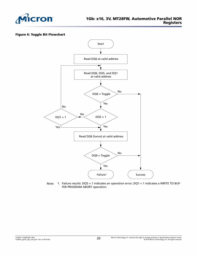
Figure 6: Toggle Bit Flowchart
DQ6 = Toggle
DQ5 = 1
DQ6 = Toggle
No
No
Yes
Yes
Yes
Start
Read DQ6 at valid address
Read DQ6, DQ5, and DQ1at valid address
Read DQ6 (twice) at valid address
SuccessFailure1
DQ1 = 1No
Yes
No
Note: 1. Failure results: DQ5 = 1 indicates an operation error; DQ1 = 1 indicates a WRITE TO BUF-FER PROGRAM ABORT operation.
1Gb: x16, 3V, MT28FW, Automotive Parallel NORRegisters
CCMTD-1725822587-3365mt28fw_genB_1gb_auto.pdf - Rev. H 05/18 EN 20 Micron Technology, Inc. reserves the right to change products or specifications without notice.
© 2014 Micron Technology, Inc. All rights reserved.
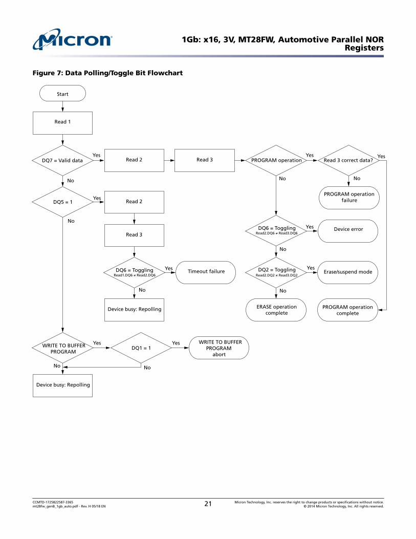
Figure 7: Data Polling/Toggle Bit Flowchart
WRITE TO BUFFERPROGRAM
Start
DQ7 = Valid data
DQ5 = 1
Yes
No
No
Yes
Yes
DQ6 = Toggling Yes
No No
No
Yes
PROGRAM operation
No
No
DQ6 = Toggling
No
DQ2 = Toggling
Yes
Yes
Yes
DQ1 = 1
Read 3 correct data?
No
Yes
Read 1
Read 2
Read 2
Read 3
Device busy: Repolling
Device busy: Repolling
Read 3
PROGRAM operationcomplete
PROGRAM operationfailure
WRITE TO BUFFERPROGRAM
abort
Timeout failure
ERASE operationcomplete
Erase/suspend mode
Device errorRead2.DQ6 = Read3.DQ6
Read2.DQ2 = Read3.DQ2Read1.DQ6 = Read2.DQ6
1Gb: x16, 3V, MT28FW, Automotive Parallel NORRegisters
CCMTD-1725822587-3365mt28fw_genB_1gb_auto.pdf - Rev. H 05/18 EN 21 Micron Technology, Inc. reserves the right to change products or specifications without notice.
© 2014 Micron Technology, Inc. All rights reserved.
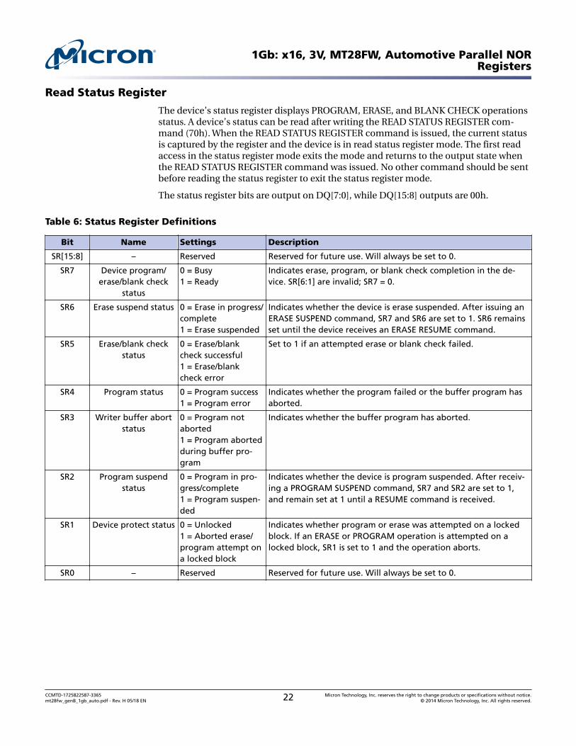
Read Status Register
The device’s status register displays PROGRAM, ERASE, and BLANK CHECK operationsstatus. A device’s status can be read after writing the READ STATUS REGISTER com-mand (70h). When the READ STATUS REGISTER command is issued, the current statusis captured by the register and the device is in read status register mode. The first readaccess in the status register mode exits the mode and returns to the output state whenthe READ STATUS REGISTER command was issued. No other command should be sentbefore reading the status register to exit the status register mode.
The status register bits are output on DQ[7:0], while DQ[15:8] outputs are 00h.
Table 6: Status Register Definitions
Bit Name Settings Description
SR[15:8] – Reserved Reserved for future use. Will always be set to 0.
SR7 Device program/erase/blank check
status
0 = Busy1 = Ready
Indicates erase, program, or blank check completion in the de-vice. SR[6:1] are invalid; SR7 = 0.
SR6 Erase suspend status 0 = Erase in progress/complete1 = Erase suspended
Indicates whether the device is erase suspended. After issuing anERASE SUSPEND command, SR7 and SR6 are set to 1. SR6 remainsset until the device receives an ERASE RESUME command.
SR5 Erase/blank checkstatus
0 = Erase/blankcheck successful1 = Erase/blankcheck error
Set to 1 if an attempted erase or blank check failed.
SR4 Program status 0 = Program success1 = Program error
Indicates whether the program failed or the buffer program hasaborted.
SR3 Writer buffer abortstatus
0 = Program notaborted1 = Program abortedduring buffer pro-gram
Indicates whether the buffer program has aborted.
SR2 Program suspendstatus
0 = Program in pro-gress/complete1 = Program suspen-ded
Indicates whether the device is program suspended. After receiv-ing a PROGRAM SUSPEND command, SR7 and SR2 are set to 1,and remain set at 1 until a RESUME command is received.
SR1 Device protect status 0 = Unlocked1 = Aborted erase/program attempt ona locked block
Indicates whether program or erase was attempted on a lockedblock. If an ERASE or PROGRAM operation is attempted on alocked block, SR1 is set to 1 and the operation aborts.
SR0 – Reserved Reserved for future use. Will always be set to 0.
1Gb: x16, 3V, MT28FW, Automotive Parallel NORRegisters
CCMTD-1725822587-3365mt28fw_genB_1gb_auto.pdf - Rev. H 05/18 EN 22 Micron Technology, Inc. reserves the right to change products or specifications without notice.
© 2014 Micron Technology, Inc. All rights reserved.
Clear Status Register
The status register content can be cleared by CLEAR STATUS REGISTER command(71h). The CLEAR STATUS REGISTER command clears the status register bits SR[6:1].SR7 remains at 0, which indicates the device is busy.
However, for buffer program abort only, the CLEAR STATUS REGISTER commandwould change also SR7 to 1, which reverts the device to main array read mode. The sta-tus register can also be cleared by using RESET Command (F0h).
1Gb: x16, 3V, MT28FW, Automotive Parallel NORRegisters
CCMTD-1725822587-3365mt28fw_genB_1gb_auto.pdf - Rev. H 05/18 EN 23 Micron Technology, Inc. reserves the right to change products or specifications without notice.
© 2014 Micron Technology, Inc. All rights reserved.
Lock Register
Table 7: Lock Register Bit Definitions
Note 1 applies to entire tableBit Name Settings Description Notes
DQ[15:9] – Default value = 1 DQ[15:9] are reserved and are set to a default value of 1.
DQ8 – Default value = 0 DQ8 is reserved and is set to a default value of 0.
DQ[7:3] – Default value =1 DQ[7:3] are reserved and are set to a default value of 1.
DQ2 Password pro-tection mode
lock bit
0 = Password protec-tion mode enabled1 = Password protec-tion mode disabled(default)
Places the device permanently in password protection mode. 2
DQ1 Nonvolatileprotection
mode lock bit
0 = Nonvolatile pro-tection mode enabledwith password protec-tion mode perma-nently disabled1 = Nonvolatile pro-tection mode enabled(default)
Places the device in nonvolatile protection mode, with pass-word protection mode permanently disabled. When shippedfrom the factory, the device will operate in nonvolatile pro-tection mode, and the memory blocks are unprotected.
2
DQ0 Extendedmemory
block protec-tion bit
0 = Protected1 = Unprotected (de-fault)
If the device is shipped with the extended memory block un-locked, the block can be protected by setting this bit to 0. Theextended memory block protection status can be read in autoselect mode by issuing an AUTO SELECT command.
Notes: 1. The lock register is a 16-bit, one-time programmable register. DQ[15:3] are reserved.2. The password protection mode lock bit and nonvolatile protection mode lock bit cannot
both be programmed to 0. Any attempt to program one while the other is programmedcauses the operation to abort, and the device returns to read mode. The device is ship-ped from the factory with the default setting.
1Gb: x16, 3V, MT28FW, Automotive Parallel NORRegisters
CCMTD-1725822587-3365mt28fw_genB_1gb_auto.pdf - Rev. H 05/18 EN 24 Micron Technology, Inc. reserves the right to change products or specifications without notice.
© 2014 Micron Technology, Inc. All rights reserved.
Figure 8: Lock Register Program Flowchart
Start
Success: EXIT PROTECTIONcommand set
Address/data cycle 1Address/data cycle 2
Done?
Match expectedvalue, 0?
No
No
Yes
Yes
Enter LOCK REGISTER command setAddress/data (unlock) cycle 1Address/data (unlock) cycle 2
Address/data cycle 3
PROGRAM LOCK REGISTERAddress/data cycle 1Address/data cycle 2
Polling algorithm
Read lock register
Notes: 1. Each lock register bit can be programmed only once.2. See the Block Protection Command Definitions table for address-data cycle details.3. DQ5 and DQ1 are ignored in this algorithm flow.
1Gb: x16, 3V, MT28FW, Automotive Parallel NORRegisters
CCMTD-1725822587-3365mt28fw_genB_1gb_auto.pdf - Rev. H 05/18 EN 25 Micron Technology, Inc. reserves the right to change products or specifications without notice.
© 2014 Micron Technology, Inc. All rights reserved.
Standard Command Definitions – Address-Data Cycles
Table 8: Standard Command Definitions – Address-Data Cycles
Note 1 applies to entire table
Command andCode/Subcode
Address and Data Cycles
Notes
1st 2nd 3rd 4th 5th 6th
A D A D A D A D A D A D
READ and AUTO SELECT Operations
READ/RESET (F0h) 555 AA 2AA 55 X F0 2
READ CFI (98h) 555 98
EXIT READ CFI (F0h) X F0
AUTO SELECT (90h) 555 AA 2AA 55 555 90 Note 3 Note 3 4, 5
EXIT AUTO SELECT (F0h) X F0
READ STATUS (70h) 555 70
CLEAR STATUS (71h) 555 71
BYPASS Operations
UNLOCK BYPASS (20h) 555 AA 2AA 55 555 20
UNLOCK BYPASSRESET (90h/00h)
X 90 X 00
PROGRAM Operations
PROGRAM (A0h) 555 AA 2AA 55 555 A0 PA PD
UNLOCK BYPASSPROGRAM (A0h)
X A0 PA PD 6
WRITE TO BUFFERPROGRAM (25h)
555 AA 2AA 55 BAd 25 BAd N PA PD 7, 8, 9
UNLOCK BYPASSWRITE TO BUFFERPROGRAM (25h)
BAd 25 BAd N PA PD 6
WRITE TO BUFFERPROGRAM CONFIRM(29h)
BAd 29 7
BUFFERED PROGRAMABORT and RESET (F0h)
555 AA 2AA 55 555 F0
PROGRAM SUSPEND(B0h)
X B0
PROGRAM RESUME (30h) X 30
PROGRAM SUSPEND(51h)
X 51
PROGRAM RESUME (50h) X 50
ERASE Operations
CHIP ERASE (80/10h) 555 AA 2AA 55 555 80 555 AA 2AA 55 555 10
UNLOCK BYPASSCHIP ERASE (80/10h)
X 80 X 10 6
1Gb: x16, 3V, MT28FW, Automotive Parallel NORStandard Command Definitions – Address-Data Cycles
CCMTD-1725822587-3365mt28fw_genB_1gb_auto.pdf - Rev. H 05/18 EN 26 Micron Technology, Inc. reserves the right to change products or specifications without notice.
© 2014 Micron Technology, Inc. All rights reserved.
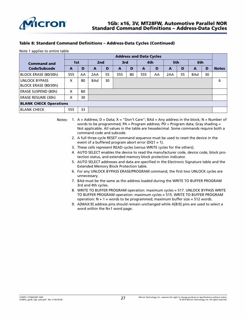
Table 8: Standard Command Definitions – Address-Data Cycles (Continued)
Note 1 applies to entire table
Command andCode/Subcode
Address and Data Cycles
Notes
1st 2nd 3rd 4th 5th 6th
A D A D A D A D A D A D
BLOCK ERASE (80/30h) 555 AA 2AA 55 555 80 555 AA 2AA 55 BAd 30
UNLOCK BYPASSBLOCK ERASE (80/30h)
X 80 BAd 30 6
ERASE SUSPEND (B0h) X B0
ERASE RESUME (30h) X 30
BLANK CHECK Operations
BLANK CHECK 555 33
Notes: 1. A = Address; D = Data; X = "Don't Care"; BAd = Any address in the block; N = Number ofwords to be programmed; PA = Program address; PD = Program data; Gray shading =Not applicable. All values in the table are hexadecimal. Some commands require both acommand code and subcode.
2. A full three-cycle RESET command sequence must be used to reset the device in theevent of a buffered program abort error (DQ1 = 1).
3. These cells represent READ cycles (versus WRITE cycles for the others).4. AUTO SELECT enables the device to read the manufacturer code, device code, block pro-
tection status, and extended memory block protection indicator.5. AUTO SELECT addresses and data are specified in the Electronic Signature table and the
Extended Memory Block Protection table.6. For any UNLOCK BYPASS ERASE/PROGRAM command, the first two UNLOCK cycles are
unnecessary.7. BAd must be the same as the address loaded during the WRITE TO BUFFER PROGRAM
3rd and 4th cycles.8. WRITE TO BUFFER PROGRAM operation: maximum cycles = 517. UNLOCK BYPASS WRITE
TO BUFFER PROGRAM operation: maximum cycles = 515. WRITE TO BUFFER PROGRAMoperation: N + 1 = words to be programmed; maximum buffer size = 512 words.
9. A[MAX:9] address pins should remain unchanged while A[8:0] pins are used to select aword within the N+1 word page.
1Gb: x16, 3V, MT28FW, Automotive Parallel NORStandard Command Definitions – Address-Data Cycles
CCMTD-1725822587-3365mt28fw_genB_1gb_auto.pdf - Rev. H 05/18 EN 27 Micron Technology, Inc. reserves the right to change products or specifications without notice.
© 2014 Micron Technology, Inc. All rights reserved.
READ and AUTO SELECT Operations
READ/RESET Command
The READ/RESET (F0h) command returns the device to read mode and resets the errorsin the data polling register. One or three bus WRITE operations can be used to issue theREAD/RESET command. Note: A full three-cycle RESET command sequence must beused to reset the device in the event of a buffered program abort error (DQ1 = 1).
Once a PROGRAM, ERASE, or SUSPEND operation begins, RESET commands are ignor-ed until the operation is complete. Read/reset serves primarily to return the device toread mode from a failed PROGRAM or ERASE operation. Read/reset may cause a returnto read mode from undefined states that might result from invalid command sequen-ces. A hardware reset may be required to return to normal operation from some unde-fined states.
To exit the unlock bypass mode, the system must issue a two-cycle UNLOCK BYPASSRESET command sequence. A READ/RESET command will not exit unlock bypassmode.
READ CFI Command
The READ CFI (98h) command puts the device in read CFI mode and is only valid whenthe device is in read array or auto select mode. One bus WRITE cycle is required to issuethe command.
Once in read CFI mode, bus READ operations will output data from the CFI memoryarea (Refer to the Common Flash Interface for details).
Read CFI mode is exited by performing a READ/RESET command (F0h). The device re-turns to read mode unless it entered read CFI mode after an ERASE SUSPEND or PRO-GRAM SUSPEND command, in which case it returns to erase or program suspendmode.
AUTO SELECT Command
At power-up or after a hardware reset, the device is in read mode. It can then be put inauto select mode by issuing an AUTO SELECT (90h) command. Auto select mode ena-bles the following device information to be read:
• Electronic signature, which includes manufacturer and device code information asshown in the Electronic Signature table.
• Block protection, which includes the block protection status and extended memoryblock protection indicator, as shown in the Block Protection table.
Electronic signature or block protection information is read by executing a READ opera-tion with control signals and addresses set, as shown in the Read Electronic Signaturetable or the Block Protection table, respectively. In addition, this device information canbe read or set by issuing an AUTO SELECT command.
Auto select mode can be used by the programming equipment to automatically match adevice with the application code to be programmed.
Three consecutive bus WRITE operations are required to issue an AUTO SELECT com-mand. The device remains in auto select mode until a READ/RESET or READ CFI com-mand is issued.
1Gb: x16, 3V, MT28FW, Automotive Parallel NORREAD and AUTO SELECT Operations
CCMTD-1725822587-3365mt28fw_genB_1gb_auto.pdf - Rev. H 05/18 EN 28 Micron Technology, Inc. reserves the right to change products or specifications without notice.
© 2014 Micron Technology, Inc. All rights reserved.
The device cannot enter auto select mode when a PROGRAM or ERASE operation is inprogress (RY/BY# LOW). However, auto select mode can be entered if the PROGRAM orERASE operation has been suspended by issuing a PROGRAM SUSPEND or ERASE SUS-PEND command.
Auto select mode is exited by performing a READ/RESET command (F0h). The devicereturns to read mode unless it entered auto select mode after an ERASE SUSPEND orPROGRAM SUSPEND command, in which case it returns to erase or program suspendmode.
Table 9: Block Protection
Note 1 applies to entire table
READ Cycle CE# OE# WE#
Address Input Data Input/Output
A[MAX:16] A[15:2] A1 A0 DQ[15:0]
128-bit (0x0~0x7) Factory-Programmable Extended Memory Protection Indicator (Bit DQ7)
Low lock L L H L L H H 0009h2
0089h3
High lock L L H L L H H 0019h2
0099h3
Block protection status
Protected L L H Block baseaddress
L H L 0001h
Unprotected L L H L H L 0000h
Notes: 1. H = Logic level HIGH (VIH); L = Logic level LOW (VIL); X = HIGH or LOW.2. Customer-lockable (default).3. Micron prelocked.
Read Electronic Signature
Table 10: Read Electronic Signature – 1Gb
Note 1 applies to entire table
READ Cycle CE# OE# WE#
Address InputData Input/
Output
A[MAX:4] A3 A2 A1 A0 DQ[15:0]
Manufacturer code L L H L L L L L 0089h
Device code 1 L L H L L L L H 227Eh
Device code 2 L L H L H H H L 2228h
Device code 3 L L H L H H H H 2201h
Note: 1. H = Logic level HIGH (VIH); L = Logic level LOW (VIL); X = HIGH or LOW.
1Gb: x16, 3V, MT28FW, Automotive Parallel NORREAD and AUTO SELECT Operations
CCMTD-1725822587-3365mt28fw_genB_1gb_auto.pdf - Rev. H 05/18 EN 29 Micron Technology, Inc. reserves the right to change products or specifications without notice.
© 2014 Micron Technology, Inc. All rights reserved.
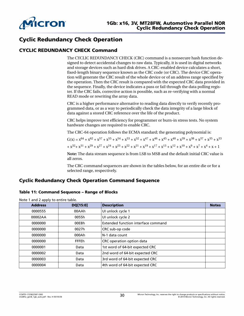
Cyclic Redundancy Check Operation
CYCLIC REDUNDANCY CHECK Command
The CYCLIC REDUNDANCY CHECK (CRC) command is a nonsecure hash function de-signed to detect accidental changes to raw data. Typically, it is used in digital networksand storage devices such as hard disk drives. A CRC-enabled device calculates a short,fixed-length binary sequence known as the CRC code (or CRC). The device CRC opera-tion will generate the CRC result of the whole device or of an address range specified bythe operation. Then the CRC result is compared with the expected CRC data provided inthe sequence. Finally, the device indicates a pass or fail through the data polling regis-ter. If the CRC fails, corrective action is possible, such as re-verifying with a normalREAD mode or rewriting the array data.
CRC is a higher performance alternative to reading data directly to verify recently pro-grammed data, or as a way to periodically check the data integrity of a large block ofdata against a stored CRC reference over the life of the product.
CRC helps improve test efficiency for programmer or burn-in stress tests. No systemhardware changes are required to enable CRC.
The CRC-64 operation follows the ECMA standard; the generating polynomial is:
G(x) = x64 + x62 + x57 + x55 + x54 + x53 + x52 + x47 + x46 + x45 + x40 + x39 + x38 + x37 + x35 + x33
+ x32+ x31 + x29 + x27 + x24 + x23 + x22 + x21 + x19 + x17 + x13 + x12 + x10 + x9 + x7 + x4 + x + 1
Note: The data stream sequence is from LSB to MSB and the default initial CRC value isall zeros.
The CRC command sequences are shown in the tables below, for an entire die or for aselected range, respectively.
Cyclic Redundancy Check Operation Command Sequence
Table 11: Command Sequence – Range of Blocks
Note 1 and 2 apply to entire table.Address DQ[15:0] Description Notes
0000555 00AAh UI unlock cycle 1
00002AA 0055h UI unlock cycle 2
0000000 00EBh Extended function interface command
0000000 0027h CRC sub-op code
0000000 000Ah N-1 data count
0000000 FFFEh CRC operation option data
0000001 Data 1st word of 64-bit expected CRC
0000002 Data 2nd word of 64-bit expected CRC
0000003 Data 3rd word of 64-bit expected CRC
0000004 Data 4th word of 64-bit expected CRC
1Gb: x16, 3V, MT28FW, Automotive Parallel NORCyclic Redundancy Check Operation
CCMTD-1725822587-3365mt28fw_genB_1gb_auto.pdf - Rev. H 05/18 EN 30 Micron Technology, Inc. reserves the right to change products or specifications without notice.
© 2014 Micron Technology, Inc. All rights reserved.
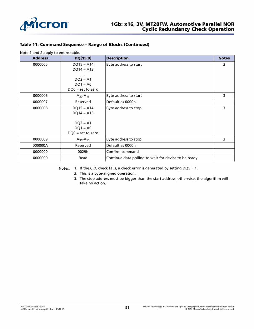
Table 11: Command Sequence – Range of Blocks (Continued)
Note 1 and 2 apply to entire table.Address DQ[15:0] Description Notes
0000005 DQ15 = A14DQ14 = A13
...DQ2 = A1DQ1 = A0
DQ0 = set to zero
Byte address to start 3
0000006 A30-A15 Byte address to start 3
0000007 Reserved Default as 0000h
0000008 DQ15 = A14DQ14 = A13
...DQ2 = A1DQ1 = A0
DQ0 = set to zero
Byte address to stop 3
0000009 A30-A15 Byte address to stop 3
000000A Reserved Default as 0000h
0000000 0029h Confirm command
0000000 Read Continue data polling to wait for device to be ready
Notes: 1. If the CRC check fails, a check error is generated by setting DQ5 = 1.2. This is a byte-aligned operation.3. The stop address must be bigger than the start address; otherwise, the algorithm will
take no action.
1Gb: x16, 3V, MT28FW, Automotive Parallel NORCyclic Redundancy Check Operation
CCMTD-1725822587-3365mt28fw_genB_1gb_auto.pdf - Rev. H 05/18 EN 31 Micron Technology, Inc. reserves the right to change products or specifications without notice.
© 2014 Micron Technology, Inc. All rights reserved.
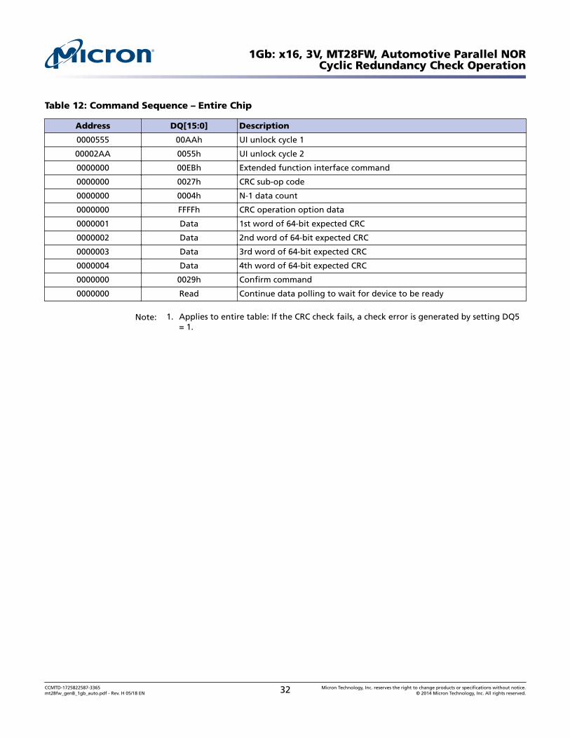
Table 12: Command Sequence – Entire Chip
Address DQ[15:0] Description
0000555 00AAh UI unlock cycle 1
00002AA 0055h UI unlock cycle 2
0000000 00EBh Extended function interface command
0000000 0027h CRC sub-op code
0000000 0004h N-1 data count
0000000 FFFFh CRC operation option data
0000001 Data 1st word of 64-bit expected CRC
0000002 Data 2nd word of 64-bit expected CRC
0000003 Data 3rd word of 64-bit expected CRC
0000004 Data 4th word of 64-bit expected CRC
0000000 0029h Confirm command
0000000 Read Continue data polling to wait for device to be ready
Note: 1. Applies to entire table: If the CRC check fails, a check error is generated by setting DQ5= 1.
1Gb: x16, 3V, MT28FW, Automotive Parallel NORCyclic Redundancy Check Operation
CCMTD-1725822587-3365mt28fw_genB_1gb_auto.pdf - Rev. H 05/18 EN 32 Micron Technology, Inc. reserves the right to change products or specifications without notice.
© 2014 Micron Technology, Inc. All rights reserved.
Bypass Operations
UNLOCK BYPASS Command
The UNLOCK BYPASS (20h) command is used to place the device in unlock bypassmode. Three bus WRITE operations are required to issue the UNLOCK BYPASS com-mand.
When the device enters unlock bypass mode, the two initial UNLOCK cycles requiredfor a standard PROGRAM or ERASE operation are not needed, thus enabling faster totalprogram or erase time.
The UNLOCK BYPASS command is used in conjunction with UNLOCK BYPASS PRO-GRAM or UNLOCK BYPASS ERASE commands to program or erase the device fasterthan with standard PROGRAM or ERASE commands. Using these commands can saveconsiderable time when the cycle time to the device is long. When in unlock bypassmode, only the following commands are valid:
• The UNLOCK BYPASS PROGRAM command can be issued to program addresseswithin the device.
• The UNLOCK BYPASS BLOCK ERASE command can then be issued to erase one ormore memory blocks.
• The UNLOCK BYPASS CHIP ERASE command can be issued to erase the whole mem-ory array.
• The UNLOCK BYPASS WRITE TO BUFFER PROGRAM and UNLOCK BYPASS EN-HANCED WRITE TO BUFFER PROGRAM commands can be issued to speed up theprogramming operation.
• The UNLOCK BYPASS RESET command can be issued to return the device to readmode.
In unlock bypass mode, the device can be read as if in read mode.
In addition to the UNLOCK BYPASS command, when VPP/WP# is raised to VHH, the de-vice automatically enters unlock bypass mode. When V PP/WP# returns to VIH or VIL, thedevice is no longer in unlock bypass mode, and normal operation resumes. The transi-tions from VIH to VHH and from VHH to VIH must be slower than tVHVPP. (See the Accel-erated Program, Data Polling/Toggle AC Characteristics.)
Note: Micron recommends entering and exiting unlock bypass mode using the ENTERUNLOCK BYPASS and UNLOCK BYPASS RESET commands rather than raising VPP/WP#to VHH. VPP/WP# should never be raised to VPPH from any mode except read mode; oth-erwise, the device may be left in an indeterminate state. VPP/WP# should not remain atVHH for than 80 hours cumulative.
UNLOCK BYPASS RESET Command
The UNLOCK BYPASS RESET (90/00h) command is used to return to read/reset modefrom unlock bypass mode. Two bus WRITE operations are required to issue the UN-LOCK BYPASS RESET command. The READ/RESET command does not exit from un-lock bypass mode.
1Gb: x16, 3V, MT28FW, Automotive Parallel NORBypass Operations
CCMTD-1725822587-3365mt28fw_genB_1gb_auto.pdf - Rev. H 05/18 EN 33 Micron Technology, Inc. reserves the right to change products or specifications without notice.
© 2014 Micron Technology, Inc. All rights reserved.
Program Operations
PROGRAM Command
The PROGRAM (A0h) command can be used to program a value to one address in thememory array. The command requires four bus WRITE operations, and the final WRITEoperation latches the address and data in the internal state machine and starts the pro-gram/erase controller. After programming has started, bus READ operations output thedata polling register content.
Programming can be suspended and then resumed by issuing a PROGRAM SUSPENDcommand and a PROGRAM RESUME command, respectively.
If the address falls in a protected block, the PROGRAM command is ignored, and thedata remains unchanged. The data polling register is not read, and no error condition isgiven.
After the PROGRAM operation has completed, the device returns to read mode, unlessan error has occurred. When an error occurs, bus READ operations to the device contin-ue to output the data polling register. A READ/RESET command must be issued to resetthe error condition and return the device to read mode.
The PROGRAM command cannot change a bit set to 0 back to 1, and an attempt to doso is masked during a PROGRAM operation. Instead, an ERASE command must be usedto set all bits in one memory block or in the entire memory from 0 to 1.
The PROGRAM operation is aborted by performing a hardware reset or by poweringdown the device. In this case, data integrity cannot be ensured, and it is recommendedthat the words or bytes that were aborted be reprogrammed.
UNLOCK BYPASS PROGRAM Command
When the device is in unlock bypass mode, the UNLOCK BYPASS PROGRAM (A0h)command can be used to program one address in the memory array. The command re-quires two bus WRITE operations instead of four required by a standard PROGRAMcommand; the final WRITE operation latches the address and data and starts the pro-gram/erase controller (The standard PROGRAM command requires four bus WRITE op-erations). The PROGRAM operation using the UNLOCK BYPASS PROGRAM commandbehaves identically to the PROGRAM operation using the PROGRAM command. Theoperation cannot be aborted. A bus READ operation to the memory outputs the datapolling register.
WRITE TO BUFFER PROGRAM Command
The WRITE TO BUFFER PROGRAM (25h) command makes use of the program buffer tospeed up programming and dramatically reduces system programming time comparedto the standard non-buffered PROGRAM command. This product supports a 512-wordmaximum program buffer.
When issuing a WRITE TO BUFFER PROGRAM command, V PP/WP# can be held HIGHor raised to VHH. Also, it can be held LOW if the block is not the lowest or highest block,depending on the part number.
The following successive steps are required to issue the WRITE TO BUFFER PROGRAMcommand:
1Gb: x16, 3V, MT28FW, Automotive Parallel NORProgram Operations
CCMTD-1725822587-3365mt28fw_genB_1gb_auto.pdf - Rev. H 05/18 EN 34 Micron Technology, Inc. reserves the right to change products or specifications without notice.
© 2014 Micron Technology, Inc. All rights reserved.
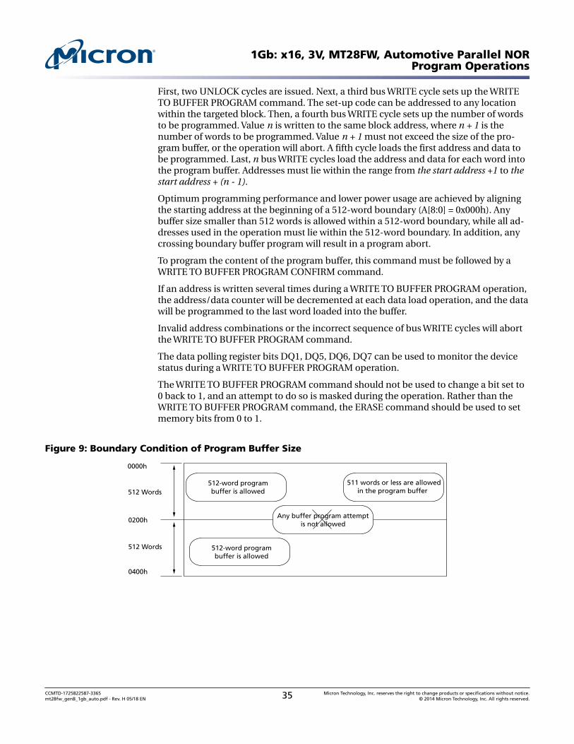
First, two UNLOCK cycles are issued. Next, a third bus WRITE cycle sets up the WRITETO BUFFER PROGRAM command. The set-up code can be addressed to any locationwithin the targeted block. Then, a fourth bus WRITE cycle sets up the number of wordsto be programmed. Value n is written to the same block address, where n + 1 is thenumber of words to be programmed. Value n + 1 must not exceed the size of the pro-gram buffer, or the operation will abort. A fifth cycle loads the first address and data tobe programmed. Last, n bus WRITE cycles load the address and data for each word intothe program buffer. Addresses must lie within the range from the start address +1 to thestart address + (n - 1).
Optimum programming performance and lower power usage are achieved by aligningthe starting address at the beginning of a 512-word boundary (A[8:0] = 0x000h). Anybuffer size smaller than 512 words is allowed within a 512-word boundary, while all ad-dresses used in the operation must lie within the 512-word boundary. In addition, anycrossing boundary buffer program will result in a program abort.
To program the content of the program buffer, this command must be followed by aWRITE TO BUFFER PROGRAM CONFIRM command.
If an address is written several times during a WRITE TO BUFFER PROGRAM operation,the address/data counter will be decremented at each data load operation, and the datawill be programmed to the last word loaded into the buffer.
Invalid address combinations or the incorrect sequence of bus WRITE cycles will abortthe WRITE TO BUFFER PROGRAM command.
The data polling register bits DQ1, DQ5, DQ6, DQ7 can be used to monitor the devicestatus during a WRITE TO BUFFER PROGRAM operation.
The WRITE TO BUFFER PROGRAM command should not be used to change a bit set to0 back to 1, and an attempt to do so is masked during the operation. Rather than theWRITE TO BUFFER PROGRAM command, the ERASE command should be used to setmemory bits from 0 to 1.
Figure 9: Boundary Condition of Program Buffer Size
0400h
0000h
512 Words
512 Words
0200h
511 words or less are allowedin the program buffer
512-word programbuffer is allowed
Any buffer program attemptis not allowed
512-word programbuffer is allowed
1Gb: x16, 3V, MT28FW, Automotive Parallel NORProgram Operations
CCMTD-1725822587-3365mt28fw_genB_1gb_auto.pdf - Rev. H 05/18 EN 35 Micron Technology, Inc. reserves the right to change products or specifications without notice.
© 2014 Micron Technology, Inc. All rights reserved.
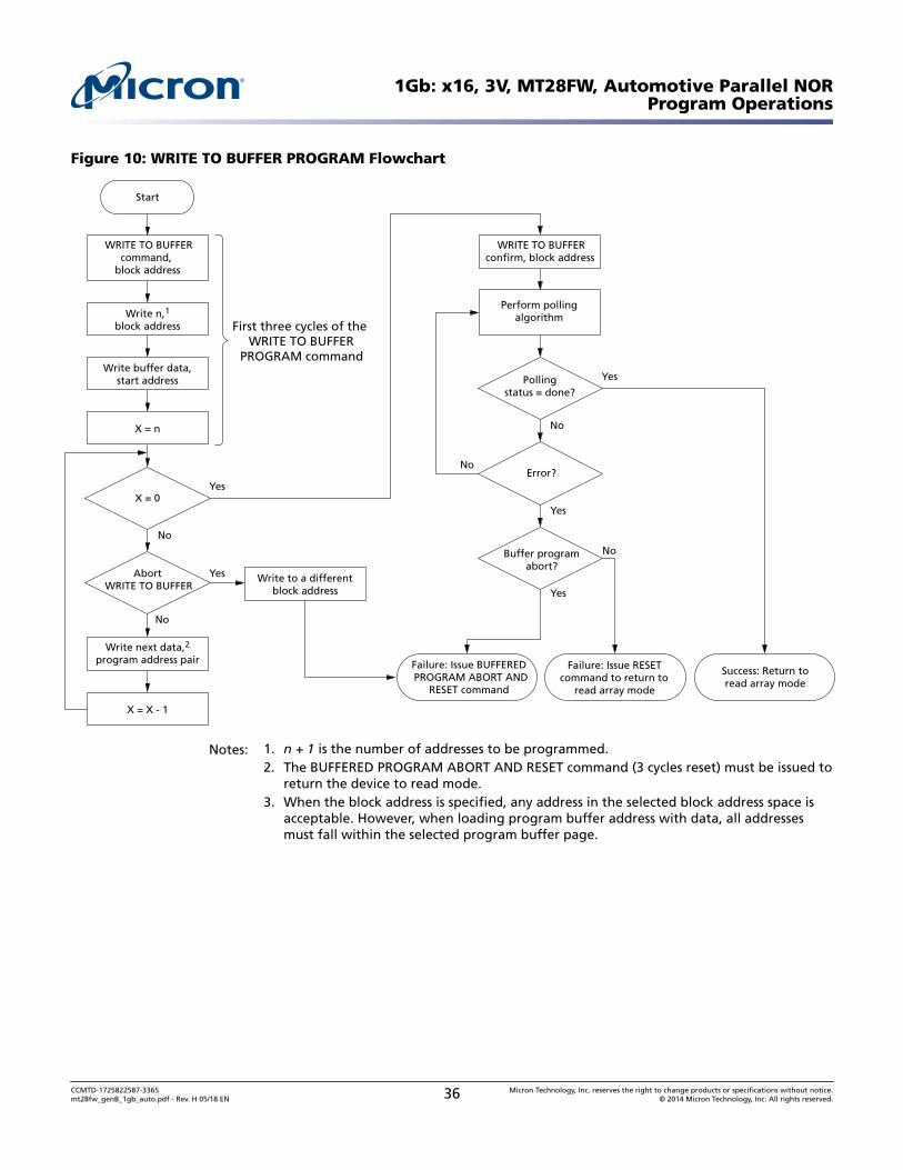
Figure 10: WRITE TO BUFFER PROGRAM Flowchart
AbortWRITE TO BUFFER
Write buffer data,start address
Start
X = n
Write n,1
block address
Write to a differentblock address
X = 0
Write next data,2
program address pair
WRITE TO BUFFERconfirm, block address
X = X - 1
Yes
No
Yes
No
Pollingstatus = done?
No
Yes
Yes
Error?No
Yes
WRITE TO BUFFERcommand,
block address
Perform pollingalgorithm
Buffer programabort?
No
Failure: Issue RESETcommand to return to
read array mode
Success: Return toread array mode
Failure: Issue BUFFEREDPROGRAM ABORT AND
RESET command
First three cycles of theWRITE TO BUFFER
PROGRAM command
Notes: 1. n + 1 is the number of addresses to be programmed.2. The BUFFERED PROGRAM ABORT AND RESET command (3 cycles reset) must be issued to
return the device to read mode.3. When the block address is specified, any address in the selected block address space is
acceptable. However, when loading program buffer address with data, all addressesmust fall within the selected program buffer page.
1Gb: x16, 3V, MT28FW, Automotive Parallel NORProgram Operations
CCMTD-1725822587-3365mt28fw_genB_1gb_auto.pdf - Rev. H 05/18 EN 36 Micron Technology, Inc. reserves the right to change products or specifications without notice.
© 2014 Micron Technology, Inc. All rights reserved.
UNLOCK BYPASS WRITE TO BUFFER PROGRAM Command
When the device is in unlock bypass mode, the UNLOCK BYPASS WRITE TO BUFFER(25h) command can be used to program the device in fast program mode. The com-mand requires two bus WRITE operations fewer than the standard WRITE TO BUFFERPROGRAM command.
The UNLOCK BYPASS WRITE TO BUFFER PROGRAM command behaves the same wayas the WRITE TO BUFFER PROGRAM command: the operation cannot be aborted, anda bus READ operation to the memory outputs the data polling register.
The WRITE TO BUFFER PROGRAM CONFIRM command is used to confirm an UN-LOCK BYPASS WRITE TO BUFFER PROGRAM command and to program the n + 1words loaded in the program buffer by this command.
WRITE TO BUFFER PROGRAM CONFIRM Command
The WRITE TO BUFFER PROGRAM CONFIRM (29h) command is used to confirm aWRITE TO BUFFER PROGRAM command and to program the n + 1 words loaded in theprogram buffer by this command.
BUFFERED PROGRAM ABORT AND RESET Command
A BUFFERED PROGRAM ABORT AND RESET (F0h) command must be issued to resetthe device to read mode when the BUFFER PROGRAM operation is aborted. The bufferprogramming sequence can be aborted in the following ways:
• Load a value that is greater than the page buffer size during the number of locationsto program in the WRITE TO BUFFER PROGRAM command.
• Write to an address in a different block than the one specified during the WRITE BUF-FER LOAD command.
• Write an address/data pair to a different write buffer page than the one selected bythe starting address during the program buffer data loading stage of the operation.
• Write data other than the CONFIRM command after the specified number of dataload cycles.
The abort condition is indicated by DQ1 = 1, DQ7 = DQ7# (for the last address locationloaded), DQ6 = toggle, and DQ5 = 0 (all of which are data polling register bits). A BUF-FERED PROGRAM ABORT and RESET command sequence must be written to reset thedevice for the next operation.
Note: The full three-cycle BUFFERED PROGRAM ABORT and RESET command se-quence is required when using buffer programming features in unlock bypass mode.
PROGRAM SUSPEND Command
The PROGRAM SUSPEND command can be used to interrupt a program operation sothat data can be read from another block. When the PROGRAM SUSPEND command isissued during a program operation, the device suspends the operation within the pro-gram suspend latency time and updates the data polling register bits.
After the PROGRAM operation has been suspended, data can be read from any address.However, data is invalid when read from an address where a program operation hasbeen suspended.
1Gb: x16, 3V, MT28FW, Automotive Parallel NORProgram Operations
CCMTD-1725822587-3365mt28fw_genB_1gb_auto.pdf - Rev. H 05/18 EN 37 Micron Technology, Inc. reserves the right to change products or specifications without notice.
© 2014 Micron Technology, Inc. All rights reserved.
The PROGRAM SUSPEND command may also be issued during a PROGRAM operationwhile an erase is suspended. In this case, data may be read from any address not inerase suspend or program suspend mode. To read from the extended memory blockarea (one-time programmable area), the ENTER/EXIT EXTENDED MEMORY BLOCKcommand sequences must be issued.
The system may also issue the AUTO SELECT command sequence when the device is inprogram suspend mode. The system can read as many auto select codes as required.When the device exits auto select mode, the device reverts to program suspend modeand is ready for another valid operation.
The PROGRAM SUSPEND operation is aborted by performing a device reset or power-down. In this case, data integrity cannot be ensured, and it is recommended that thewords that were aborted be reprogrammed. This device has two different command co-des for program suspend, B0h and 51h. Code B0h is available for legacy compatibility.Code 51h is recommended for use.
PROGRAM RESUME Command
The PROGRAM RESUME command must be issued to exit a program suspend modeand resume a PROGRAM operation. The controller can use DQ7 or DQ6 data pollingbits to determine the status of the PROGRAM operation. After a PROGRAM RESUMEcommand is issued, subsequent PROGRAM RESUME commands are ignored. AnotherPROGRAM SUSPEND command can be issued after the device has resumed program-ming. This device has two different command codes for Program Resume (30h or 50h).Code 30h is available for legacy compatibility. Code 50h is recommended to use.
ACCELERATED BUFFERED PROGRAM Operations
ACCELERATED BUFFER PROGRAM operations provides faster performance thanstandard program command sequences. Operations are enabled through VPP/WP# un-der the VHH voltage supply.
When the system asserts VHH on input, the device automatically enters the UNLOCKBYPASS mode, which enables the system to use the UNLOCK BYPASS WRITE TO BUF-FER PROGRAM (25h) command sequence.
Removing VHH from the VPP upon completion of the embedded program operation re-turns the device to normal operation.
Table 13: ACCELERATED PROGRAM Requirements and Recommendations
Device State Requirements/Recommendations
Device blocks Requirement: Must be unprotected prior to raising VPP/WP# to VHH
VHH applied to VPP/WP# Requirement: Maximum cumulative period of 80 hours.
VPP/WP# Requirement: Must not be at VHH for operations except ACCELERATED BUFFERED PRO-GRAM and CHIP ERASE; otherwise device can be damaged
Recommendation: Keep stable to VHH during ACCELERATED BUFFERED PROGRAM opera-tion
Power-up Recommendation: Apply VHH on VPP/WP# after VCC/VCCQ is stable on.
Power-down Recommendation: Adjust VPP/WP# from VHH to VIH/VIL before VCC/VCCQ goes LOW.
1Gb: x16, 3V, MT28FW, Automotive Parallel NORProgram Operations
CCMTD-1725822587-3365mt28fw_genB_1gb_auto.pdf - Rev. H 05/18 EN 38 Micron Technology, Inc. reserves the right to change products or specifications without notice.
© 2014 Micron Technology, Inc. All rights reserved.
Erase Operations
CHIP ERASE Command
The CHIP ERASE (80/10h) command erases the entire chip. Six bus WRITE operationsare required to issue the command and start the program/erase controller.
Protected blocks are not erased. If all blocks are protected, the data remains unchanged.No error is reported when protected blocks are not erased.
During the CHIP ERASE operation, the device ignores all other commands, includingERASE SUSPEND. It is not possible to abort the operation. All bus READ operations dur-ing CHIP ERASE output the data polling register on the data I/Os. See the Data PollingRegister section for more details.
After the CHIP ERASE operation completes, the device returns to read mode, unless anerror has occurred. If an error occurs, the device will continue to output the data pollingregister.
When the operation fails, a READ/RESET command must be issued to reset the errorcondition and return to read mode. The status of the array must be confirmed throughthe BLANK CHECK operation and the BLOCK ERASE command re-issued to the failedblock.
The CHIP ERASE command sets all of the bits in unprotected blocks of the device to 1.All previous data is lost.
The operation is aborted by performing a reset or by powering down the device. In thiscase, data integrity cannot be ensured, and it is recommended that the entire chip beerased again.
UNLOCK BYPASS CHIP ERASE Command
When the device is in unlock bypass mode, the UNLOCK BYPASS CHIP ERASE (80/10h)command can be used to erase all memory blocks at one time. The command requiresonly two bus WRITE operations instead of six using the standard CHIP ERASE com-mand. The final bus WRITE operation starts the program/erase controller.
The UNLOCK BYPASS CHIP ERASE command behaves the same way as the CHIPERASE command: the operation cannot be aborted, and a bus READ operation to thememory outputs the data polling register.
BLOCK ERASE Command
The BLOCK ERASE (80/30h) command erase one block. It sets all bits in the unprotec-ted selected block to 1. All previous data in the selected block are lost. Six bus WRITEoperations are required to select the block to be erased.
After the sixth bus WRITE operation, a bus READ operation outputs the data pollingregister. See the WE#-Controlled Program waveforms for details on how to identify if theprogram/erase controller has started the BLOCK ERASE operation.
After the BLOCK ERASE operation completes, the device returns to read mode, unlessan error has occurred. If an error occurs, bus READ operations will continue to outputthe data polling register. A READ/RESET command must be issued to reset the errorcondition and return to read mode.
1Gb: x16, 3V, MT28FW, Automotive Parallel NORErase Operations
CCMTD-1725822587-3365mt28fw_genB_1gb_auto.pdf - Rev. H 05/18 EN 39 Micron Technology, Inc. reserves the right to change products or specifications without notice.
© 2014 Micron Technology, Inc. All rights reserved.
If the selected block is protected, it is ignored and the data remains unchanged. No er-ror condition is given when protected block is not erased.
During the BLOCK ERASE operation, the device ignores all commands except theERASE SUSPEND command and the READ STATUS command. The operation is abor-ted by performing a hardware reset or powering down the device. In this case, data in-tegrity cannot be ensured, and it is recommended that the aborted blocks be erasedagain.
UNLOCK BYPASS BLOCK ERASE Command
When the device is in unlock bypass mode, the UNLOCK BYPASS BLOCK ERASE(80/30h) command can be used to erase one memory block. The command requirestwo bus WRITE operations instead of six using the standard BLOCK ERASE command.The final bus WRITE operation latches the address of the block and starts the program/erase controller.
The UNLOCK BYPASS BLOCK ERASE command behaves the same way as the BLOCKERASE command: the operation cannot be aborted, and a bus READ operation to thememory outputs the data polling register. See the BLOCK ERASE Command section fordetails.
ERASE SUSPEND Command
The ERASE SUSPEND (B0h) command temporarily suspends a BLOCK ERASE opera-tion. One bus WRITE operation is required to issue the command. The block address is"Don't Care."
The program/erase controller suspends the ERASE operation within the erase suspendlatency time of the ERASE SUSPEND command being issued. However, when theERASE SUSPEND command is written during the block erase timeout, the device im-mediately terminates the timeout period and suspends the ERASE operation. After theprogram/erase controller has stopped, the device operates in read mode, and the eraseis suspended.
During an ERASE SUSPEND operation, it is possible to execute these operations in ar-rays that are not suspended:
• READ (main memory array)• PROGRAM• WRITE TO BUFFER PROGRAM• AUTO SELECT• READ CFI• UNLOCK BYPASS• Extended memory block commands• READ/RESET
Reading from a suspended block will output the data polling register. If an attempt ismade to program in a protected or suspended block, the PROGRAM command is ignor-ed and the data remains unchanged; also, the data polling register is not read and noerror condition is given.
Before the RESUME command is initiated, the READ/RESET command must to issuedto exit AUTO SELECT and READ CFI operations. In addition, the EXIT UNLOCK BYPASS
1Gb: x16, 3V, MT28FW, Automotive Parallel NORErase Operations
CCMTD-1725822587-3365mt28fw_genB_1gb_auto.pdf - Rev. H 05/18 EN 40 Micron Technology, Inc. reserves the right to change products or specifications without notice.
© 2014 Micron Technology, Inc. All rights reserved.
and EXIT EXTENDED MEMORY BLOCK commands must be issued to exit unlock by-pass and the extended memory block modes.
An ERASE SUSPEND command is ignored if it is written during a CHIP ERASE opera-tion.
If the ERASE SUSPEND operation is aborted by performing a device hardware reset orpower-down, data integrity cannot be ensured, and it is recommended that the suspen-ded blocks be erased again.
ERASE RESUME Command
The ERASE RESUME (30h) command restarts the program/erase controller after anERASE SUSPEND operation.
The device must be in read array mode before the RESUME command will be accepted.An erase can be suspended and resumed more than once.
ACCELERATED CHIP ERASE OperationsThe ACCELERATED CHIP ERASE operation provides faster performance than thestandard CHIP ERASE command sequence. Operations are enabled through VPP/WP#under the VHH voltage supply.
When the system asserts VHH on input, the device automatically enters the UNLOCKBYPASS mode, which enables the system to use the UNLOCK BYPASS CHIP ERASE(80/30h) command sequence.
When a block is protected, the CHIP ERASE command skips the protected block andcontinues with next block erase. The command algorithm skips a block that failed toerase and continues with the remaining blocks. The fail flag will be set for the operation.
Removing VHH from the VPP/WP# upon completion of the embedded erase operationreturns the device to normal operation. When an error occurs or when the operationfails, the array status should be confirmed through the BLANK CHECK operation andthe BLOCK ERASE command re-issued to the failed block.
Table 14: ACCELERATED CHIP ERASE Requirements and Recommendations
Device Component/State Requirements/Recommendations
VPP/WP# Requirement: Must not be at VHH for operations except ACCELERATED PROGRAM andCHIP ERASE; otherwise device can be damaged.
VHH applied to VPP/WP# Requirement: Maximum cumulative period of 80 hours.
Power-up Recommendation: Apply VHH on VPP/WP# after VCC/VCCQ is stable on.
Power-down Recommendation: Adjust VPP/WP# from VHH to VIH/VIL before VCC/VCCQ goes LOW.
BLANK CHECK OperationThe BLANK CHECK operation determines whether a specified block is blank (that is,completely erased). It can also be used to determine whether a previous ERASE opera-tion was successful, including ERASE operations that might have been interrupted bypower loss.
1Gb: x16, 3V, MT28FW, Automotive Parallel NORACCELERATED CHIP ERASE Operations
CCMTD-1725822587-3365mt28fw_genB_1gb_auto.pdf - Rev. H 05/18 EN 41 Micron Technology, Inc. reserves the right to change products or specifications without notice.
© 2014 Micron Technology, Inc. All rights reserved.
The BLANK CHECK operation checks for cells that are programmed or over-erased. If itfinds any, it returns a failure status, indicating that the block is not blank. If it returns apassing status, the block is guaranteed blank (all 1s) and is ready to program.
Before executing, the ERASE operation initiates an embedded BLANK CHECK opera-tion, and if the target block is blank, the ERASE operation is skipped, benefitting overallcycle performance; otherwise, the ERASE operation continues.
The BLANK CHECK operation can occur in only one block at a time, and during its exe-cution, reading the data polling register is the only other operation allowed. Readingfrom any address in the device enables reading the data polling register to monitorblank check progress or errors. Operations such as READ (array data), PROGRAM,ERASE, and any suspended operation are not allowed.
After the BLANK CHECK operation has completed, the device returns to read mode un-less an error has occurred. When an error occurs, the device continues to output datapolling register data. A READ/RESET command must be issued to reset the error condi-tion and return the device to read mode.
1Gb: x16, 3V, MT28FW, Automotive Parallel NORBLANK CHECK Operation
CCMTD-1725822587-3365mt28fw_genB_1gb_auto.pdf - Rev. H 05/18 EN 42 Micron Technology, Inc. reserves the right to change products or specifications without notice.
© 2014 Micron Technology, Inc. All rights reserved.
Device Protection
Hardware Protection
The VPP/WP# function provides a hardware method of protecting either the highest orlowest block. When V PP/WP# is LOW, PROGRAM and ERASE operations on either ofthese block options is ignored to provide protection. When V PP/WP# is HIGH, the de-vice reverts to the previous protection status for the highest or lowest block. PROGRAMand ERASE operations can modify the data in either of these block options unless blockprotection is enabled.
Note: Micron highly recommends driving VPP/WP# HIGH or LOW. If a system needs tofloat the VPP/WP# pin, without a pull-up/pull-down resistor and no capacitor, then aninternal pull-up resistor is enabled.
Table 15: VPP/WP# Functions
VPP/WP# Settings Function
VIL Highest or lowest block is protected.
VIH Highest or lowest block is unprotected unless software protection is activated.
Software Protection
The following software protection modes are available:
• Volatile protection• Nonvolatile protection• Password protection
The device is shipped with all blocks unprotected. On first use, the device defaults tothe nonvolatile protection mode but can be activated in either the nonvolatile protec-tion or password protection mode.
The desired protection mode is activated by setting either the nonvolatile protectionmode lock bit or the password protection mode lock bit of the lock register (see the LockRegister section). Both bits are one-time-programmable and nonvolatile; therefore, af-ter the protection mode has been activated, it cannot be changed, and the device is setpermanently to operate in the selected protection mode. It is recommended that thedesired software protection mode be activated when first programming the device.
For the highest or lowest block, a higher level of block protection can be achieved bylocking the block using nonvolatile protection mode and holding VPP /WP# LOW.
Blocks with volatile protection and nonvolatile protection can coexist within the memo-ry array. If the user attempts to program or erase a protected block, the device ignoresthe command and returns to read mode.
The block protection status can be read by performing a read electronic signature or byissuing an AUTO SELECT command (see the Block Protection table).
Refer to the Block Protection Status table and the Software Protection Scheme figure fordetails on the block protection scheme. Refer to the Protection Operations section for adescription of the command sets.
1Gb: x16, 3V, MT28FW, Automotive Parallel NORDevice Protection
CCMTD-1725822587-3365mt28fw_genB_1gb_auto.pdf - Rev. H 05/18 EN 43 Micron Technology, Inc. reserves the right to change products or specifications without notice.
© 2014 Micron Technology, Inc. All rights reserved.
Volatile Protection Mode
Volatile protection enables the software application to protect blocks against inadver-tent change and can be disabled when changes are needed. Volatile protection bits areunique for each block and can be individually modified. Volatile protection bits controlthe protection scheme only for unprotected blocks whose nonvolatile protection bitsare cleared to 1. Issuing a PROGRAM VOLATILE PROTECTION BIT or CLEAR VOLATILEPROTECTION BIT command sets to 0 or clears to 1 the volatile protection bits and pla-ces the associated blocks in the protected (0) or unprotected (1) state, respectively. Thevolatile protection bit can be set or cleared as often as needed.
When the device is first shipped, or after a power-up or hardware reset, the volatile pro-tection bits default to 1 (unprotected).
Nonvolatile Protection Mode
A nonvolatile protection bit is assigned to each block. Each of these bits can be set forprotection individually by issuing a PROGRAM NONVOLATILE PROTECTION BIT com-mand. Also, each device has one global volatile bit called the nonvolatile protection bitlock bit; it can be set to protect all nonvolatile protection bits at once. This global bitmust be set to 0 only after all nonvolatile protection bits are configured to the desiredsettings. When set to 0, the nonvolatile protection bit lock bit prevents changes to thestate of the nonvolatile protection bits. When cleared to 1, the nonvolatile protectionbits can be set and cleared using the PROGRAM NONVOLATILE PROTECTION BIT andCLEAR ALL NONVOLATILE PROTECTION BITS commands, respectively.
No software command unlocks the nonvolatile protection bit lock bit unless the deviceis in password protection mode; in nonvolatile protection mode, the nonvolatile protec-tion bit lock bit can be cleared only by taking the device through a hardware reset orpower-up.
Nonvolatile protection bits cannot be cleared individually; they must be cleared all atonce using a CLEAR ALL NONVOLATILE PROTECTION BITS command. They will re-main set through a hardware reset or a power-down/power-up sequence.
If one of the nonvolatile protection bits needs to be cleared (unprotected), additionalsteps are required: First, the nonvolatile protection bit lock bit must be cleared to 1, us-ing either a power-cycle or hardware reset. Then, the nonvolatile protection bits can bechanged to reflect the desired settings. Finally, the nonvolatile protection bit lock bitmust be set to 0 to lock the nonvolatile protection bits. The device now will operate nor-mally.
To achieve the best protection, the PROGRAM NONVOLATILE PROTECTION LOCK BITcommand should be executed early in the boot code, and the boot code should be pro-tected by holding VPP/WP# LOW.
Nonvolatile protection bits and volatile protection bits have the same function whenVPP/WP# is HIGH or when VPP/WP# is at the voltage for program acceleration (VHH ).
Password Protection Mode
The password protection mode provides a higher level of security than the nonvolatileprotection mode by requiring a 64-bit password to unlock the nonvolatile protection bitlock bit. In addition to this password requirement, the nonvolatile protection bit lockbit is set to 0 after power-up and reset to maintain the device in password protectionmode.
1Gb: x16, 3V, MT28FW, Automotive Parallel NORDevice Protection
CCMTD-1725822587-3365mt28fw_genB_1gb_auto.pdf - Rev. H 05/18 EN 44 Micron Technology, Inc. reserves the right to change products or specifications without notice.
© 2014 Micron Technology, Inc. All rights reserved.
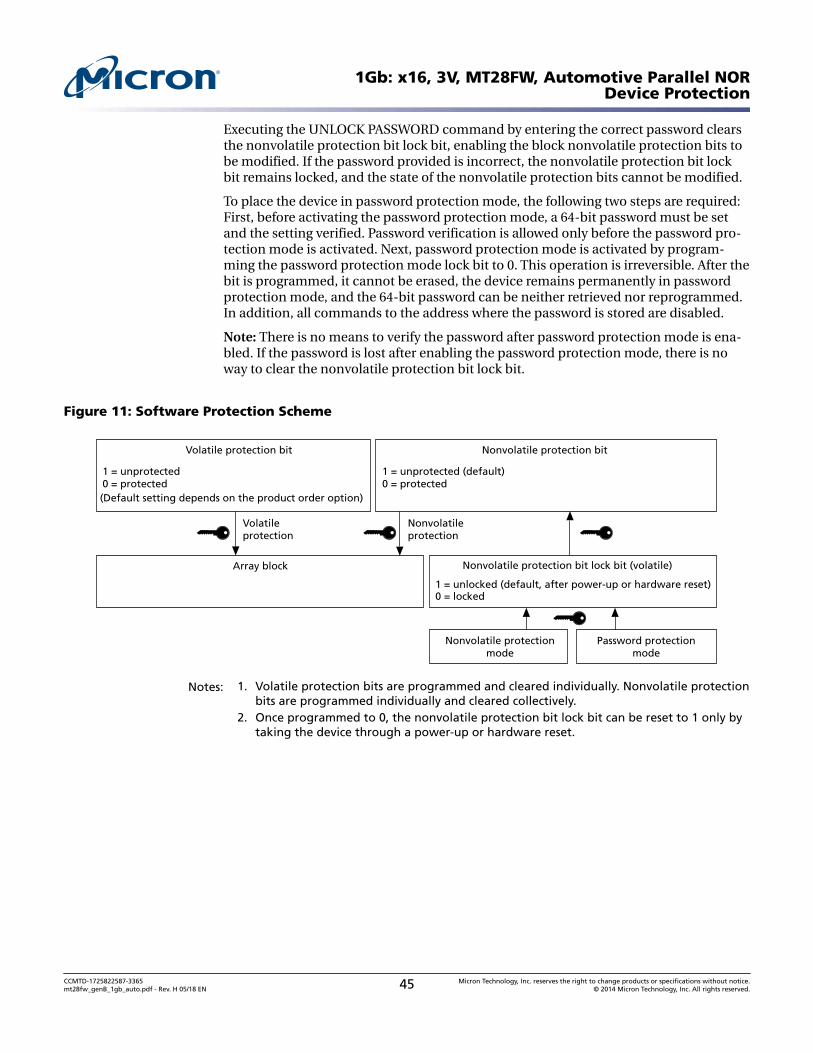
Executing the UNLOCK PASSWORD command by entering the correct password clearsthe nonvolatile protection bit lock bit, enabling the block nonvolatile protection bits tobe modified. If the password provided is incorrect, the nonvolatile protection bit lockbit remains locked, and the state of the nonvolatile protection bits cannot be modified.
To place the device in password protection mode, the following two steps are required:First, before activating the password protection mode, a 64-bit password must be setand the setting verified. Password verification is allowed only before the password pro-tection mode is activated. Next, password protection mode is activated by program-ming the password protection mode lock bit to 0. This operation is irreversible. After thebit is programmed, it cannot be erased, the device remains permanently in passwordprotection mode, and the 64-bit password can be neither retrieved nor reprogrammed.In addition, all commands to the address where the password is stored are disabled.
Note: There is no means to verify the password after password protection mode is ena-bled. If the password is lost after enabling the password protection mode, there is noway to clear the nonvolatile protection bit lock bit.
Figure 11: Software Protection Scheme
1 = unprotected (default)0 = protected
1 = unprotected0 = protected(Default setting depends on the product order option)
Volatile protection bit Nonvolatile protection bit
1 = unlocked (default, after power-up or hardware reset)0 = locked
Nonvolatile protection bit lock bit (volatile)
Nonvolatile protectionmode
Password protectionmode
Volatileprotection
Nonvolatileprotection
Array block
Notes: 1. Volatile protection bits are programmed and cleared individually. Nonvolatile protectionbits are programmed individually and cleared collectively.
2. Once programmed to 0, the nonvolatile protection bit lock bit can be reset to 1 only bytaking the device through a power-up or hardware reset.
1Gb: x16, 3V, MT28FW, Automotive Parallel NORDevice Protection
CCMTD-1725822587-3365mt28fw_genB_1gb_auto.pdf - Rev. H 05/18 EN 45 Micron Technology, Inc. reserves the right to change products or specifications without notice.
© 2014 Micron Technology, Inc. All rights reserved.
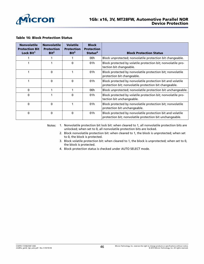
Table 16: Block Protection Status
NonvolatileProtection Bit
Lock Bit1
NonvolatileProtection
Bit2
VolatileProtection
Bit3
BlockProtection
Status4 Block Protection Status
1 1 1 00h Block unprotected; nonvolatile protection bit changeable.
1 1 0 01h Block protected by volatile protection bit; nonvolatile pro-tection bit changeable.
1 0 1 01h Block protected by nonvolatile protection bit; nonvolatileprotection bit changeable.
1 0 0 01h Block protected by nonvolatile protection bit and volatileprotection bit; nonvolatile protection bit changeable.
0 1 1 00h Block unprotected; nonvolatile protection bit unchangeable.
0 1 0 01h Block protected by volatile protection bit; nonvolatile pro-tection bit unchangeable.
0 0 1 01h Block protected by nonvolatile protection bit; nonvolatileprotection bit unchangeable.
0 0 0 01h Block protected by nonvolatile protection bit and volatileprotection bit; nonvolatile protection bit unchangeable.
Notes: 1. Nonvolatile protection bit lock bit: when cleared to 1, all nonvolatile protection bits areunlocked; when set to 0, all nonvolatile protection bits are locked.
2. Block nonvolatile protection bit: when cleared to 1, the block is unprotected; when setto 0, the block is protected.
3. Block volatile protection bit: when cleared to 1, the block is unprotected; when set to 0,the block is protected.
4. Block protection status is checked under AUTO SELECT mode.
1Gb: x16, 3V, MT28FW, Automotive Parallel NORDevice Protection
CCMTD-1725822587-3365mt28fw_genB_1gb_auto.pdf - Rev. H 05/18 EN 46 Micron Technology, Inc. reserves the right to change products or specifications without notice.
© 2014 Micron Technology, Inc. All rights reserved.
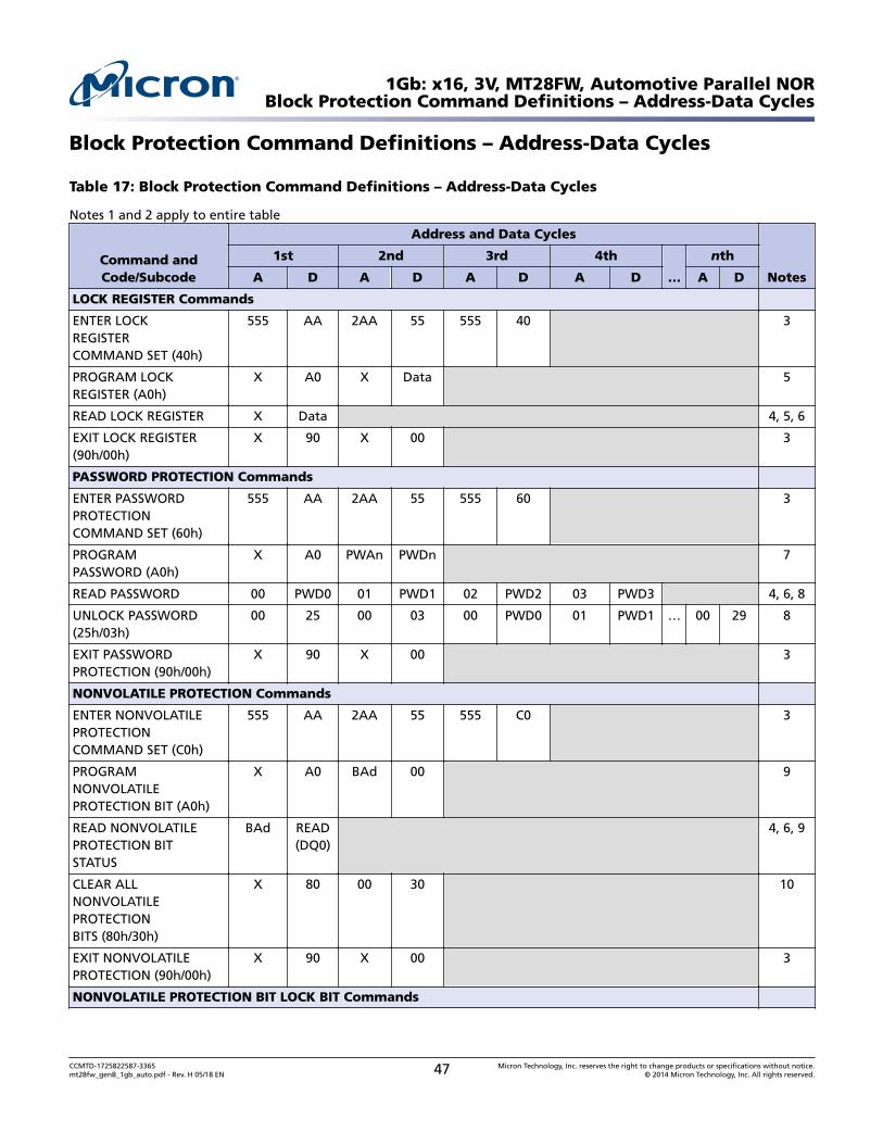
Block Protection Command Definitions – Address-Data Cycles
Table 17: Block Protection Command Definitions – Address-Data Cycles
Notes 1 and 2 apply to entire table
Command andCode/Subcode
Address and Data Cycles
Notes
1st 2nd 3rd 4th
…
nth
A D A D A D A D A D
LOCK REGISTER Commands
ENTER LOCKREGISTERCOMMAND SET (40h)
555 AA 2AA 55 555 40 3
PROGRAM LOCKREGISTER (A0h)
X A0 X Data 5
READ LOCK REGISTER X Data 4, 5, 6
EXIT LOCK REGISTER(90h/00h)
X 90 X 00 3
PASSWORD PROTECTION Commands
ENTER PASSWORDPROTECTIONCOMMAND SET (60h)
555 AA 2AA 55 555 60 3
PROGRAMPASSWORD (A0h)
X A0 PWAn PWDn 7
READ PASSWORD 00 PWD0 01 PWD1 02 PWD2 03 PWD3 4, 6, 8
UNLOCK PASSWORD(25h/03h)
00 25 00 03 00 PWD0 01 PWD1 … 00 29 8
EXIT PASSWORDPROTECTION (90h/00h)
X 90 X 00 3
NONVOLATILE PROTECTION Commands
ENTER NONVOLATILEPROTECTIONCOMMAND SET (C0h)
555 AA 2AA 55 555 C0 3
PROGRAMNONVOLATILEPROTECTION BIT (A0h)
X A0 BAd 00 9
READ NONVOLATILEPROTECTION BITSTATUS
BAd READ(DQ0)
4, 6, 9
CLEAR ALLNONVOLATILEPROTECTIONBITS (80h/30h)
X 80 00 30 10
EXIT NONVOLATILEPROTECTION (90h/00h)
X 90 X 00 3
NONVOLATILE PROTECTION BIT LOCK BIT Commands
1Gb: x16, 3V, MT28FW, Automotive Parallel NORBlock Protection Command Definitions – Address-Data Cycles
CCMTD-1725822587-3365mt28fw_genB_1gb_auto.pdf - Rev. H 05/18 EN 47 Micron Technology, Inc. reserves the right to change products or specifications without notice.
© 2014 Micron Technology, Inc. All rights reserved.
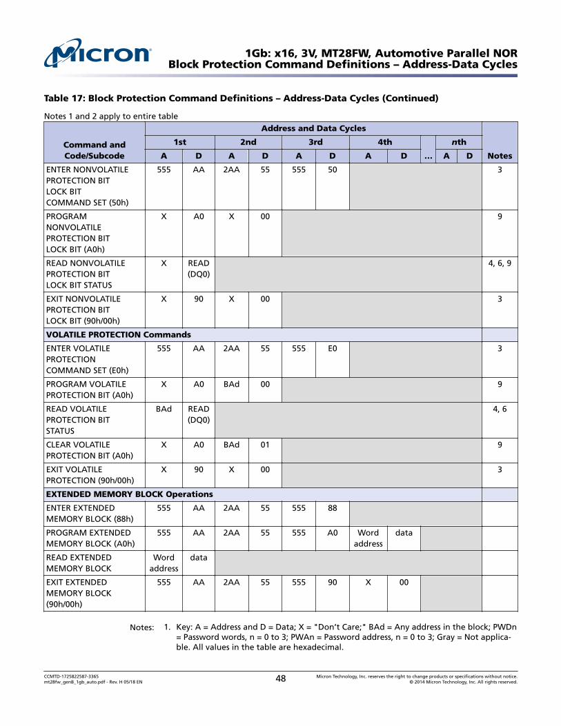
Table 17: Block Protection Command Definitions – Address-Data Cycles (Continued)
Notes 1 and 2 apply to entire table
Command andCode/Subcode
Address and Data Cycles
Notes
1st 2nd 3rd 4th
…
nth
A D A D A D A D A D
ENTER NONVOLATILEPROTECTION BITLOCK BITCOMMAND SET (50h)
555 AA 2AA 55 555 50 3
PROGRAMNONVOLATILEPROTECTION BITLOCK BIT (A0h)
X A0 X 00 9
READ NONVOLATILEPROTECTION BITLOCK BIT STATUS
X READ(DQ0)
4, 6, 9
EXIT NONVOLATILEPROTECTION BITLOCK BIT (90h/00h)
X 90 X 00 3
VOLATILE PROTECTION Commands
ENTER VOLATILEPROTECTIONCOMMAND SET (E0h)
555 AA 2AA 55 555 E0 3
PROGRAM VOLATILEPROTECTION BIT (A0h)
X A0 BAd 00 9
READ VOLATILEPROTECTION BITSTATUS
BAd READ(DQ0)
4, 6
CLEAR VOLATILEPROTECTION BIT (A0h)
X A0 BAd 01 9
EXIT VOLATILEPROTECTION (90h/00h)
X 90 X 00 3
EXTENDED MEMORY BLOCK Operations
ENTER EXTENDEDMEMORY BLOCK (88h)
555 AA 2AA 55 555 88
PROGRAM EXTENDEDMEMORY BLOCK (A0h)
555 AA 2AA 55 555 A0 Wordaddress
data
READ EXTENDEDMEMORY BLOCK
Wordaddress
data
EXIT EXTENDEDMEMORY BLOCK(90h/00h)
555 AA 2AA 55 555 90 X 00
Notes: 1. Key: A = Address and D = Data; X = "Don’t Care;" BAd = Any address in the block; PWDn= Password words, n = 0 to 3; PWAn = Password address, n = 0 to 3; Gray = Not applica-ble. All values in the table are hexadecimal.
1Gb: x16, 3V, MT28FW, Automotive Parallel NORBlock Protection Command Definitions – Address-Data Cycles
CCMTD-1725822587-3365mt28fw_genB_1gb_auto.pdf - Rev. H 05/18 EN 48 Micron Technology, Inc. reserves the right to change products or specifications without notice.
© 2014 Micron Technology, Inc. All rights reserved.
2. DQ[15:8] are "Don’t Care" during UNLOCK and COMMAND cycles. A[MAX:16] are"Don’t Care" during UNLOCK and COMMAND cycles, unless an address is required.
3. The ENTER command sequence must be issued prior to any operation. It disables READand WRITE operations from and to block 0. READ and WRITE operations from and toany other block are allowed. Also, when an ENTER COMMAND SET command is issued,an EXIT COMMAND SET command must be issued to return the device to READ mode.
4. READ REGISTER/PASSWORD commands have no command code; CE# and OE# are drivenLOW and data is read according to a specified address.
5. Data = Lock register content.6. All address cycles shown for this command are READ cycles.7. Only one portion of the password can be programmed or read by each PROGRAM PASS-
WORD command.8. Each portion of the password can be entered or read in any order as long as the entire
64-bit password is entered or read.9. Both nonvolatile and volatile protection bit settings are as follows: Protected state = 00;
Unprotected state = 01.10. The CLEAR ALL NONVOLATILE PROTECTION BITS command programs all nonvolatile pro-
tection bits before erasure. This prevents over-erasure of previously cleared nonvolatileprotection bits.
1Gb: x16, 3V, MT28FW, Automotive Parallel NORBlock Protection Command Definitions – Address-Data Cycles
CCMTD-1725822587-3365mt28fw_genB_1gb_auto.pdf - Rev. H 05/18 EN 49 Micron Technology, Inc. reserves the right to change products or specifications without notice.
© 2014 Micron Technology, Inc. All rights reserved.
Protection OperationsBlocks can be protected individually against accidental PROGRAM or ERASE opera-tions. The block protection scheme is shown in the Software Protection Scheme figure.Memory block and extended memory block protection is configured through the lockregister.
LOCK REGISTER Commands
After the ENTER LOCK REGISTER COMMAND SET (40h) command has been issued, allbus READ or PROGRAM operations can be issued to the lock register.
The PROGRAM LOCK REGISTER (A0h) command allows the lock register to be config-ured. The programmed data can then be checked with a READ LOCK REGISTER com-mand by driving CE# and OE# LOW with the appropriate address data on the addressbus.
PASSWORD PROTECTION Commands
After the ENTER PASSWORD PROTECTION COMMAND SET (60h) command has beenissued, the commands related to password protection mode can be issued to the device.
The PROGRAM PASSWORD (A0h) command is used to program the 64-bit passwordused in the password protection mode. To program the 64-bit password, the completecommand sequence must be entered four times at four consecutive addresses selectedby A[1:0]. By default, all password bits are set to 1. The password can be checked by is-suing a READ PASSWORD command.
Note: A password must be programmed per Flash memory die to enable password pro-tection.
The READ PASSWORD command is used to verify the password used in password pro-tection mode. To verify the 64-bit password, the complete command sequence must beentered four times at four consecutive addresses selected by A[1:0]. If the passwordmode lock bit is programmed and the user attempts to read the password, the devicewill output 00h onto the I/O data bus.
The UNLOCK PASSWORD (25/03h) command is used to clear the nonvolatile protec-tion bit lock bit, allowing the nonvolatile protection bits to be modified. The UNLOCKPASSWORD command must be issued, along with the correct password, and requires a6μs delay between successive UNLOCK PASSWORD commands in order to preventhackers from cracking the password by trying all possible 64-bit combinations. If thisdelay does not occur, the latest command will be ignored. Approximately 6μs is re-quired for unlocking the device after the valid 64-bit password has been provided.
NONVOLATILE PROTECTION Commands
After the ENTER NONVOLATILE PROTECTION COMMAND SET (C0h) command hasbeen issued, the commands related to nonvolatile protection mode can be issued to thedevice.
A block can be protected from program or erase by issuing a PROGRAM NONVOLATILEPROTECTION BIT (A0h) command, along with the block address. This command setsthe nonvolatile protection bit to 0 for a given block.
1Gb: x16, 3V, MT28FW, Automotive Parallel NORProtection Operations
CCMTD-1725822587-3365mt28fw_genB_1gb_auto.pdf - Rev. H 05/18 EN 50 Micron Technology, Inc. reserves the right to change products or specifications without notice.
© 2014 Micron Technology, Inc. All rights reserved.
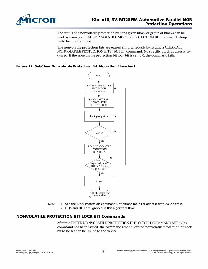
The status of a nonvolatile protection bit for a given block or group of blocks can beread by issuing a READ NONVOLATILE MODIFY PROTECTION BIT command, alongwith the block address.
The nonvolatile protection bits are erased simultaneously by issuing a CLEAR ALLNONVOLATILE PROTECTION BITS (80/30h) command. No specific block address is re-quired. If the nonvolatile protection bit lock bit is set to 0, the command fails.
Figure 12: Set/Clear Nonvolatile Protection Bit Algorithm Flowchart
No
No
Yes
Yes
Success
Done?
Matchexpected value?DQ0 = 1 (clear)
or 0 (set)
ENTER NONVOLATILE PROTECTIONcommand set
Start
PROGRAM/CLEARNONVOLATILE
PROTECTION BIT
Polling algorithm
READ NONVOLATILEPROTECTIONBIT STATUS
EXIT PROTECTIONcommand set
Notes: 1. See the Block Protection Command Definitions table for address-data cycle details.2. DQ5 and DQ1 are ignored in this algorithm flow.
NONVOLATILE PROTECTION BIT LOCK BIT Commands
After the ENTER NONVOLATILE PROTECTION BIT LOCK BIT COMMAND SET (50h)command has been issued, the commands that allow the nonvolatile protection bit lockbit to be set can be issued to the device.
1Gb: x16, 3V, MT28FW, Automotive Parallel NORProtection Operations
CCMTD-1725822587-3365mt28fw_genB_1gb_auto.pdf - Rev. H 05/18 EN 51 Micron Technology, Inc. reserves the right to change products or specifications without notice.
© 2014 Micron Technology, Inc. All rights reserved.
The PROGRAM NONVOLATILE PROTECTION BIT LOCK BIT (A0h) command is used toset the nonvolatile protection bit lock bit to 0, thus locking the nonvolatile protectionbits and preventing them from being modified.
The READ NONVOLATILE PROTECTION BIT LOCK BIT STATUS command is used toread the status of the nonvolatile protection bit lock bit.
VOLATILE PROTECTION Commands
After the ENTER VOLATILE PROTECTION COMMAND SET (E0h) command has beenissued, commands related to the volatile protection mode can be issued to the device.
The PROGRAM VOLATILE PROTECTION BIT (A0h) command individually sets a vola-tile protection bit to 0 for a given block. If the nonvolatile protection bit for the sameblock is set, the block is locked regardless of the value of the volatile protection bit (seethe Block Protection Status table).
The status of a volatile protection bit for a given block can be read by issuing a READVOLATILE PROTECTION BIT STATUS command along with the block address.
The CLEAR VOLATILE PROTECTION BIT (A0h) command individually clears (sets to 1)the volatile protection bit for a given block. If the nonvolatile protection bit for the sameblock is set, the block is locked regardless of the value of the volatile protection bit (seethe Block Protection Status table).
EXTENDED MEMORY BLOCK Commands
The device has one extra 512-word extended memory block that can be accessed onlyby the ENTER EXTENDED MEMORY BLOCK (88h) command. It is used as a securityblock to provide a permanent 128-bit secure ID number or to store additional informa-tion. The device can be shipped with the extended memory block prelocked perma-nently by Micron, including the 128-bit security identification number. Or, the devicecan be shipped with the extended memory block unlocked, enabling customers to per-manently program and lock it (default) (see Lock Register, the AUTO SELECT com-mand, and the Block Protection table.)
Table 18: Extended Memory Block Address and Data
Address
Data
Micron Prelocked Customer Lockable
000000h–000007h
Secure ID number Determined by customer (default)
000008h–0001FFh
Protected andunavailable
After the ENTER EXTENDED MEMORY BLOCK command has been issued, the deviceenters the extended memory block mode. All bus READ or PROGRAM operations areconducted on the extended memory block, and the extended memory block is ad-dressed using the addresses occupied by block 0 in the other operating modes (see theMemory Map table).
In extended memory block mode, ERASE, CHIP ERASE, ERASE SUSPEND, and ERASERESUME commands are not allowed. The extended memory block cannot be erased,and each bit of the extended memory block can only be programmed once.
1Gb: x16, 3V, MT28FW, Automotive Parallel NORProtection Operations
CCMTD-1725822587-3365mt28fw_genB_1gb_auto.pdf - Rev. H 05/18 EN 52 Micron Technology, Inc. reserves the right to change products or specifications without notice.
© 2014 Micron Technology, Inc. All rights reserved.
The extended memory block is protected from further modification by programminglock register bit 0. Once invoked, this protection cannot be undone.
The device remains in extended memory block mode until the EXIT EXTENDED MEM-ORY BLOCK (90/00h) command is issued, which returns the device to read mode, oruntil power is removed from the device. After a power-up sequence or hardware reset,the device will revert to reading memory blocks in the main array.
EXIT PROTECTION Command
The EXIT PROTECTION COMMAND SET (90/00h) command is used to exit the lockregister, password protection, nonvolatile protection, volatile protection, and nonvola-tile protection bit lock bit command set modes and return the device to read mode.
Note that the READ/RESET command (F0h) is ignored under these modes.
1Gb: x16, 3V, MT28FW, Automotive Parallel NORProtection Operations
CCMTD-1725822587-3365mt28fw_genB_1gb_auto.pdf - Rev. H 05/18 EN 53 Micron Technology, Inc. reserves the right to change products or specifications without notice.
© 2014 Micron Technology, Inc. All rights reserved.
Common Flash InterfaceThe common flash interface (CFI) is a JEDEC-approved, standardized data structurethat can be read from the flash memory device. It allows a system's software to querythe device to determine various electrical and timing parameters, density information,and functions supported by the memory. The system can interface easily with the de-vice, enabling the software to upgrade itself when necessary.
When the READ CFI command is issued, the device enters CFI query mode and the datastructure is read from memory. The following tables show the addresses (A[7:0]) used toretrieve the data. The query data is always presented on the lowest order data outputs(DQ[7:0]), and the other data outputs (DQ[15:8]) are set to 0.
Table 19: Query Structure Overview
Note 1 applies to the entire tableAddress Subsection Name Description
10h CFI query identification string Command set ID and algorithm data offset
1Bh System interface information Device timing and voltage information
27h Device geometry definition Flash device layout
40h Primary algorithm-specific extended query table Additional information specific to the primary algo-rithm (optional)
Note: 1. Query data are always presented on the lowest order data outputs (DQ[7:0]). DQ[15:8]are set to 0.
Table 20: CFI Query Identification String
Note 1 applies to the entire tableAddress Data Description Value
10h 0051h Query unique ASCII string "QRY" "Q"
11h 0052h "R"
12h 0059h "Y"
13h14h
0002h0000h
Primary algorithm command set and control interface ID code 16-bit ID code de-fining a specific algorithm
–
15h16h
0040h0000h
Address for primary algorithm extended query table (see the Primary Algorithm-Specific Extended Query Table)
P = 40h
17h18h
0000h0000h
Alternate vendor command set and control interface ID code second vendor-speci-fied algorithm supported
–
19h1Ah
0000h0000h
Address for alternate algorithm extended query table –
Note: 1. Query data are always presented on the lowest order data outputs (DQ[7:0]). DQ[15:8]are set to 0.
1Gb: x16, 3V, MT28FW, Automotive Parallel NORCommon Flash Interface
CCMTD-1725822587-3365mt28fw_genB_1gb_auto.pdf - Rev. H 05/18 EN 54 Micron Technology, Inc. reserves the right to change products or specifications without notice.
© 2014 Micron Technology, Inc. All rights reserved.

Table 21: CFI Query System Interface Information
Note 1 applies to the entire tableAddress Data Description Value
1Bh 0027h VCC logic supply minimum program/erase voltageBits[7:4] BCD value in voltsBits[3:0] BCD value in 100mV
2.7V
1Ch 0036h VCC logic supply maximum program/erase voltageBits[7:4] BCD value in voltsBits[3:0] BCD value in 100mV
3.6V
1Dh 0085h VHH (programming) supply minimum program/erase voltageBits[7:4] hex value in voltsBits[3:0] BCD value in 100mV
8.5V
1Eh 0095h VHH (programming) supply maximum program/erase voltageBits[7:4] hex value in voltsBits[3:0] BCD value in 10mV
9.5V
1Fh 0005h Typical timeout for single byte/word program = 2nμs 32µs
20h 0009h Typical timeout for maximum size buffer program = 2nμs 512µs
21h 0008h Typical timeout per individual block erase = 2nms 256ms
22h 0012h Typical timeout for full chip erase = 2nms 262s
23h 0003h Maximum timeout for byte/word program = 2n times typical 256µs
24h 0002h Maximum timeout for buffer program = 2n times typical 2048µs
25h 0003h Maximum timeout per individual block erase = 2n times typical 2s
26h 0003h Maximum timeout for chip erase = 2n times typical 2096s
Note: 1. The values in this table are valid for all packages.
Table 22: Device Geometry Definition
Address Data Description Value
27h 001Bh Device size = 2n in number of bytes 128MB
28h29h
0001h0000h
Flash device interface code description x16asynchronous
2Ah2Bh
000Ah0000h
Maximum number of bytes in multi-byte program or page = 2n 1024
2Ch 0001h Number of erase block regions. It specifies the number of regionscontaining contiguous erase blocks of the same size.
1
2Dh2Eh
00FFh0003h
Erase block region 1 informationNumber of identical-size erase blocks = 01FFh + 1
1024
2Fh30h
0000h0002h
Erase block region 1 informationBlock size in region 1 = 0200h × 256 bytes
128KB
31h32h33h34h
0000h0000h0000h0000h
Erase block region 2 information 0
1Gb: x16, 3V, MT28FW, Automotive Parallel NORCommon Flash Interface
CCMTD-1725822587-3365mt28fw_genB_1gb_auto.pdf - Rev. H 05/18 EN 55 Micron Technology, Inc. reserves the right to change products or specifications without notice.
© 2014 Micron Technology, Inc. All rights reserved.
Table 22: Device Geometry Definition (Continued)
Address Data Description Value
35h36h37h38h
0000h0000h0000h0000h
Erase block region 3 information 0
39h3Ah3Bh3Ch
0000h0000h0000h0000h
Erase block region 4 information 0
3Dh3Eh3Fh
FFFFhFFFFhFFFFh
Reserved –
Table 23: Primary Algorithm-Specific Extended Query Table
Note 1 applies to the entire tableAddress Data Description Value
40h 0050h Primary algorithm extended query table unique ASCII string “PRI” "P"
41h 0052h "R"
42h 0049h "I"
43h 0031h Major version number, ASCII "1"
44h 0035h Minor version number, ASCII "5"
45h 001Ch Address sensitive unlock (bits[1:0]):00 = Required01 = Not requiredProcess technology (bits [7:2])0111b: Second generation
Required
46h 0002h Erase suspend:00 = Not supported01 = Read only02 = Read and write
2
47h 0001h Block protection:00 = Not supportedx = Number of blocks per group
1
48h 0000h Temporary block unprotect scheme:00 = Not supported01 = Supported
Not supported
49h 0008h Protect/unprotect scheme:08 = Advanced sector protection method
8
4Ah 0000h Simultaneous operations:Not supported
–
4Bh 0000h Burst mode:00 = Not supported01 = Supported
Not supported
1Gb: x16, 3V, MT28FW, Automotive Parallel NORCommon Flash Interface
CCMTD-1725822587-3365mt28fw_genB_1gb_auto.pdf - Rev. H 05/18 EN 56 Micron Technology, Inc. reserves the right to change products or specifications without notice.
© 2014 Micron Technology, Inc. All rights reserved.
Table 23: Primary Algorithm-Specific Extended Query Table (Continued)
Note 1 applies to the entire tableAddress Data Description Value
4Ch 0003h Page mode:00 = Not supported01 = 4-word page02 = 8-word page03 = 16-word page
16-word page
4Dh 0085h VHH supply minimum program/erase voltage:Bits[7:4] hex value in voltsBits[3:0] BCD value in 100mV
8.5V
4Eh 0095h VHH supply maximum program/erase voltage:Bits[7:4] hex value in voltsBits[3:0] BCD value in 100mV
9.5V
4Fh 00xxh WP# protection:xx = 04h: Uniform device, HW protection for lowest blockxx = 05h: Uniform device, HW protection for highest block
Uniform + VPP/WP#protecting highest
or lowest block
50h 0001h Program suspend:00 = Not supported01 = Supported
Supported
51h 0001h Unlock bypass:00 = Not supported01 = Supported
Supported
52h 000Ah Extended memory block (customer OTP area): 2n bytes 1024 bytes
1Gb: x16, 3V, MT28FW, Automotive Parallel NORCommon Flash Interface
CCMTD-1725822587-3365mt28fw_genB_1gb_auto.pdf - Rev. H 05/18 EN 57 Micron Technology, Inc. reserves the right to change products or specifications without notice.
© 2014 Micron Technology, Inc. All rights reserved.
Table 23: Primary Algorithm-Specific Extended Query Table (Continued)
Note 1 applies to the entire tableAddress Data Description Value
53h 008Fh Software Features –
bit 0: Status register polling00 = Not supported01 = Supported)
bit 1: DQ polling00 = Not supported01 = Supported)
bit 2: Program suspend/resume commands00 = Not supported01 = Supported)
bit 3: Word programming00 = Not supported01 = Supported)
bit 4: Bit-field programming00 = Not supported01 = Supported)
bit 5: Autodetect programming00 = Not supported01 = Supported)
bit 6: RFU
bit 7: Multiple writes per line00 = Not supported01 = Supported)
54h 0005h Page size: 2n bytes 32 bytes
55h 0005h Erase suspend timeout maximum: 2n (µs) 32µs
56h 0004h Program suspend timeout maximum: 2n (µs) 16µs
57h to 77h FFFFh Reserved –
78h 0005h tPLRH maximum: 2n (µs) 32µs
79h 0009h tVCCPH maximum: 2n (µs)Power-on reset
512µs
Note: 1. The values in this table are valid for both packages.
1Gb: x16, 3V, MT28FW, Automotive Parallel NORCommon Flash Interface
CCMTD-1725822587-3365mt28fw_genB_1gb_auto.pdf - Rev. H 05/18 EN 58 Micron Technology, Inc. reserves the right to change products or specifications without notice.
© 2014 Micron Technology, Inc. All rights reserved.
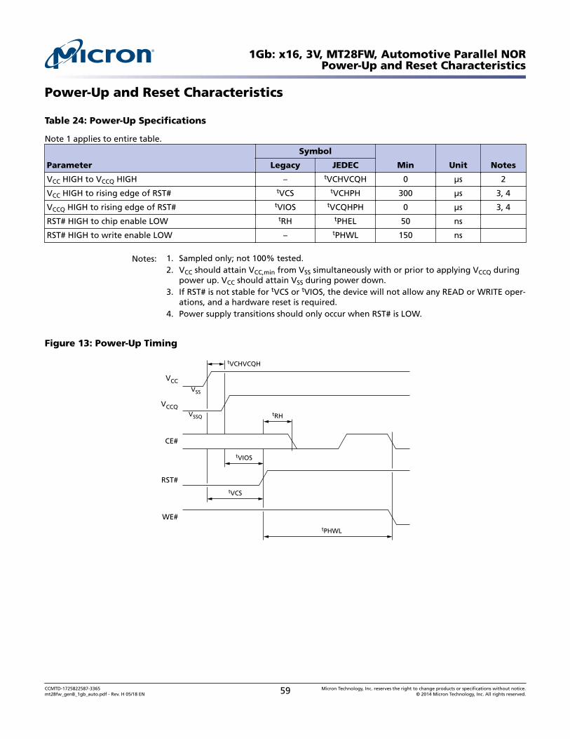
Power-Up and Reset Characteristics
Table 24: Power-Up Specifications
Note 1 applies to entire table.
Parameter
Symbol
Min Unit NotesLegacy JEDEC
VCC HIGH to VCCQ HIGH – tVCHVCQH 0 µs 2
VCC HIGH to rising edge of RST# tVCS tVCHPH 300 µs 3, 4
VCCQ HIGH to rising edge of RST# tVIOS tVCQHPH 0 µs 3, 4
RST# HIGH to chip enable LOW tRH tPHEL 50 ns
RST# HIGH to write enable LOW – tPHWL 150 ns
Notes: 1. Sampled only; not 100% tested.2. VCC should attain VCC,min from VSS simultaneously with or prior to applying VCCQ during
power up. VCC should attain VSS during power down.3. If RST# is not stable for tVCS or tVIOS, the device will not allow any READ or WRITE oper-
ations, and a hardware reset is required.4. Power supply transitions should only occur when RST# is LOW.
Figure 13: Power-Up Timing
tRH
tVIOS
tVCS
tPHWL
tVCHVCQH
VCCQ
VCC
CE#
RST#
WE#
VSSQ
VSS
1Gb: x16, 3V, MT28FW, Automotive Parallel NORPower-Up and Reset Characteristics
CCMTD-1725822587-3365mt28fw_genB_1gb_auto.pdf - Rev. H 05/18 EN 59 Micron Technology, Inc. reserves the right to change products or specifications without notice.
© 2014 Micron Technology, Inc. All rights reserved.
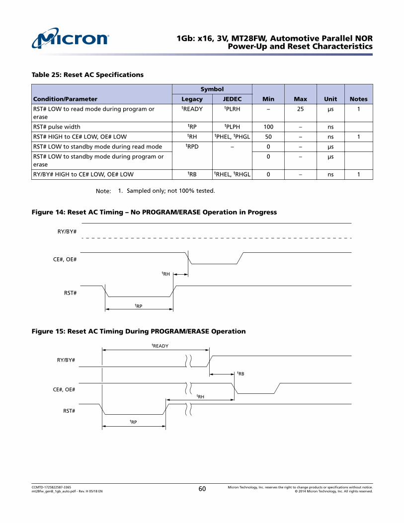
Table 25: Reset AC Specifications
Condition/Parameter
Symbol
Min Max Unit NotesLegacy JEDEC
RST# LOW to read mode during program orerase
tREADY tPLRH – 25 µs 1
RST# pulse width tRP tPLPH 100 – ns
RST# HIGH to CE# LOW, OE# LOW tRH tPHEL, tPHGL 50 – ns 1
RST# LOW to standby mode during read mode tRPD – 0 – µs
RST# LOW to standby mode during program orerase
0 – µs
RY/BY# HIGH to CE# LOW, OE# LOW tRB tRHEL, tRHGL 0 – ns 1
Note: 1. Sampled only; not 100% tested.
Figure 14: Reset AC Timing – No PROGRAM/ERASE Operation in Progress
tRH
RY/BY#
CE#, OE#
RST#
tRP
Figure 15: Reset AC Timing During PROGRAM/ERASE Operation
tRB
RY/BY#
CE#, OE#
RST#
tRP
tRH
tREADY
1Gb: x16, 3V, MT28FW, Automotive Parallel NORPower-Up and Reset Characteristics
CCMTD-1725822587-3365mt28fw_genB_1gb_auto.pdf - Rev. H 05/18 EN 60 Micron Technology, Inc. reserves the right to change products or specifications without notice.
© 2014 Micron Technology, Inc. All rights reserved.
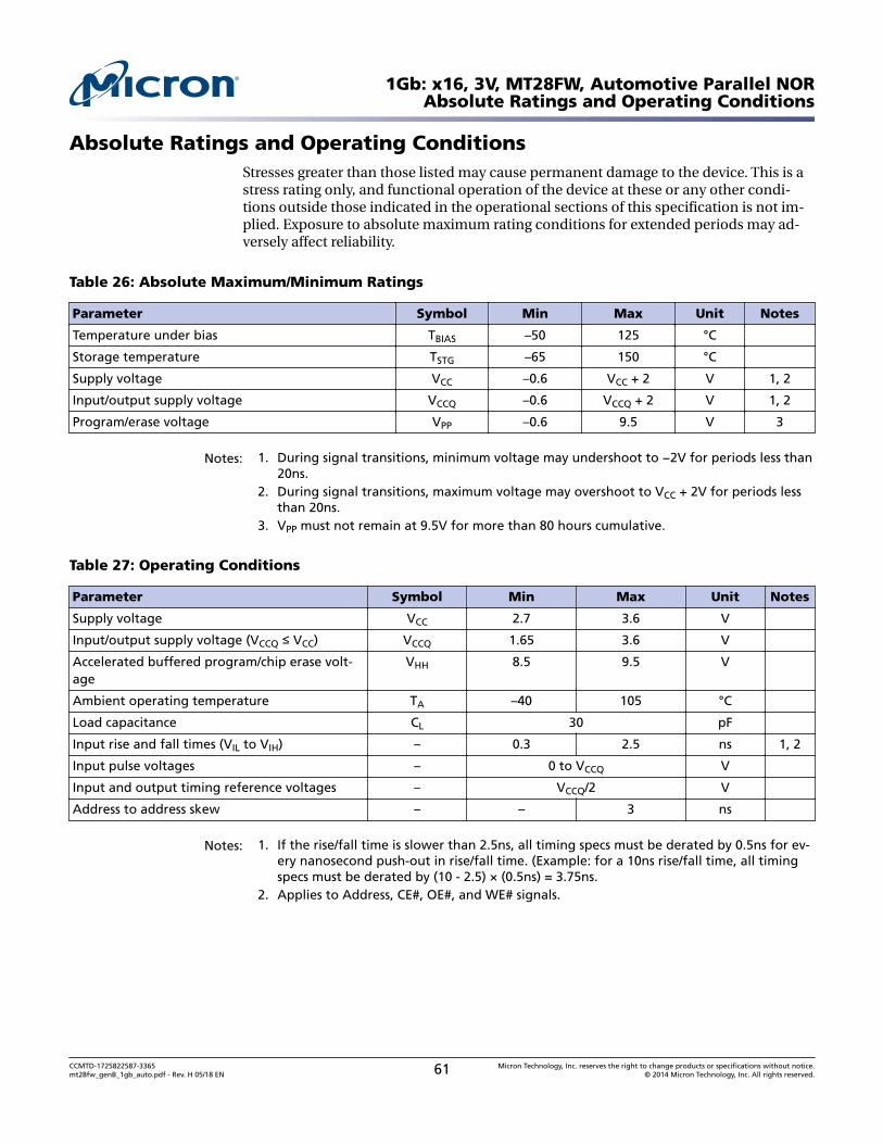
Absolute Ratings and Operating ConditionsStresses greater than those listed may cause permanent damage to the device. This is astress rating only, and functional operation of the device at these or any other condi-tions outside those indicated in the operational sections of this specification is not im-plied. Exposure to absolute maximum rating conditions for extended periods may ad-versely affect reliability.
Table 26: Absolute Maximum/Minimum Ratings
Parameter Symbol Min Max Unit Notes
Temperature under bias TBIAS –50 125 °C
Storage temperature TSTG –65 150 °C
Supply voltage VCC –0.6 VCC + 2 V 1, 2
Input/output supply voltage VCCQ –0.6 VCCQ + 2 V 1, 2
Program/erase voltage VPP –0.6 9.5 V 3
Notes: 1. During signal transitions, minimum voltage may undershoot to −2V for periods less than20ns.
2. During signal transitions, maximum voltage may overshoot to VCC + 2V for periods lessthan 20ns.
3. VPP must not remain at 9.5V for more than 80 hours cumulative.
Table 27: Operating Conditions
Parameter Symbol Min Max Unit Notes
Supply voltage VCC 2.7 3.6 V
Input/output supply voltage (VCCQ ≤ VCC) VCCQ 1.65 3.6 V
Accelerated buffered program/chip erase volt-age
VHH 8.5 9.5 V
Ambient operating temperature TA –40 105 °C
Load capacitance CL 30 pF
Input rise and fall times (VIL to VIH) – 0.3 2.5 ns 1, 2
Input pulse voltages – 0 to VCCQ V
Input and output timing reference voltages – VCCQ/2 V
Address to address skew – – 3 ns
Notes: 1. If the rise/fall time is slower than 2.5ns, all timing specs must be derated by 0.5ns for ev-ery nanosecond push-out in rise/fall time. (Example: for a 10ns rise/fall time, all timingspecs must be derated by (10 - 2.5) × (0.5ns) = 3.75ns.
2. Applies to Address, CE#, OE#, and WE# signals.
1Gb: x16, 3V, MT28FW, Automotive Parallel NORAbsolute Ratings and Operating Conditions
CCMTD-1725822587-3365mt28fw_genB_1gb_auto.pdf - Rev. H 05/18 EN 61 Micron Technology, Inc. reserves the right to change products or specifications without notice.
© 2014 Micron Technology, Inc. All rights reserved.
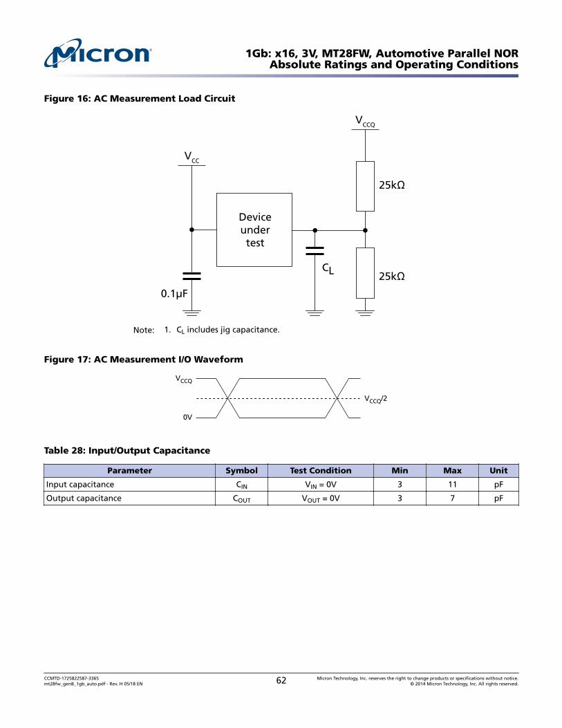
Figure 16: AC Measurement Load Circuit
CL
VCCQ
25kΩ
Deviceundertest
0.1µF
VCC
25kΩ
Note: 1. CL includes jig capacitance.
Figure 17: AC Measurement I/O Waveform
VCCQ
0V
VCCQ/2
Table 28: Input/Output Capacitance
Parameter Symbol Test Condition Min Max Unit
Input capacitance CIN VIN = 0V 3 11 pF
Output capacitance COUT VOUT = 0V 3 7 pF
1Gb: x16, 3V, MT28FW, Automotive Parallel NORAbsolute Ratings and Operating Conditions
CCMTD-1725822587-3365mt28fw_genB_1gb_auto.pdf - Rev. H 05/18 EN 62 Micron Technology, Inc. reserves the right to change products or specifications without notice.
© 2014 Micron Technology, Inc. All rights reserved.
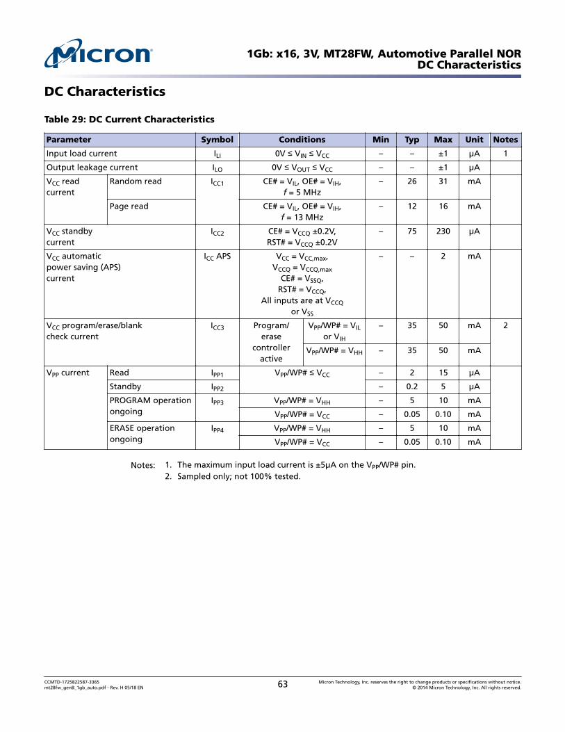
DC Characteristics
Table 29: DC Current Characteristics
Parameter Symbol Conditions Min Typ Max Unit Notes
Input load current ILI 0V ≤ VIN ≤ VCC – – ±1 µA 1
Output leakage current ILO 0V ≤ VOUT ≤ VCC – – ±1 µA
VCC readcurrent
Random read ICC1 CE# = VIL, OE# = VIH,f = 5 MHz
– 26 31 mA
Page read CE# = VIL, OE# = VIH,f = 13 MHz
– 12 16 mA
VCC standbycurrent
ICC2 CE# = VCCQ ±0.2V,RST# = VCCQ ±0.2V
– 75 230 µA
VCC automaticpower saving (APS)current
ICC APS VCC = VCC,max,VCCQ = VCCQ,max
CE# = VSSQ,RST# = VCCQ,
All inputs are at VCCQ
or VSS
– – 2 mA
VCC program/erase/blankcheck current
ICC3 Program/erase
controlleractive
VPP/WP# = VIL
or VIH
– 35 50 mA 2
VPP/WP# = VHH – 35 50 mA
VPP current Read IPP1 VPP/WP# ≤ VCC – 2 15 µA
Standby IPP2 – 0.2 5 µA
PROGRAM operationongoing
IPP3 VPP/WP# = VHH – 5 10 mA
VPP/WP# = VCC – 0.05 0.10 mA
ERASE operationongoing
IPP4 VPP/WP# = VHH – 5 10 mA
VPP/WP# = VCC – 0.05 0.10 mA
Notes: 1. The maximum input load current is ±5µA on the VPP/WP# pin.2. Sampled only; not 100% tested.
1Gb: x16, 3V, MT28FW, Automotive Parallel NORDC Characteristics
CCMTD-1725822587-3365mt28fw_genB_1gb_auto.pdf - Rev. H 05/18 EN 63 Micron Technology, Inc. reserves the right to change products or specifications without notice.
© 2014 Micron Technology, Inc. All rights reserved.
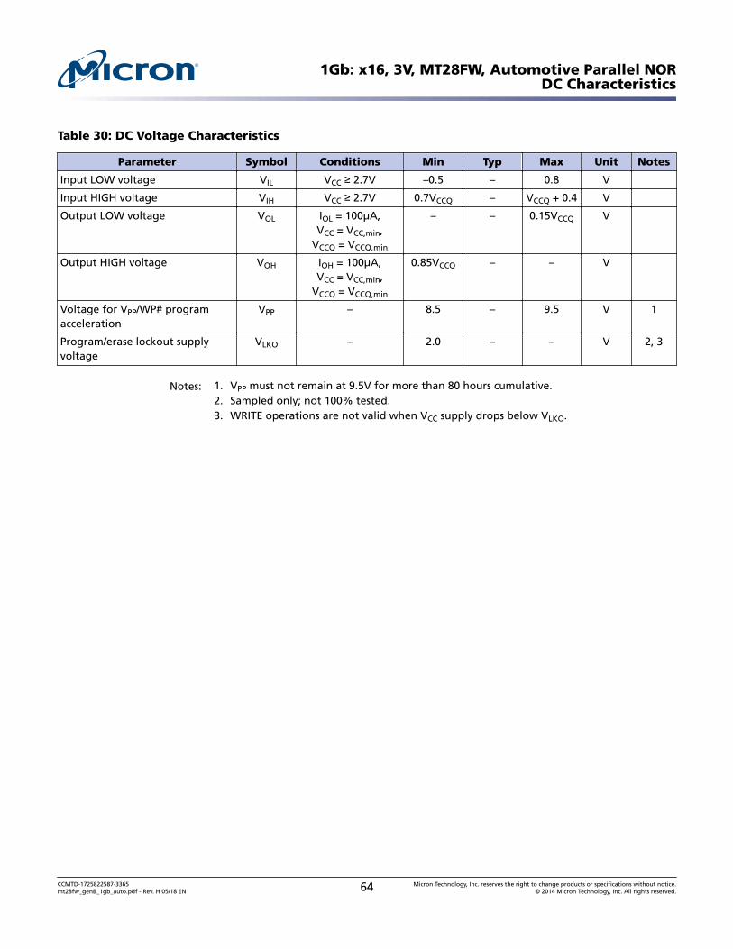
Table 30: DC Voltage Characteristics
Parameter Symbol Conditions Min Typ Max Unit Notes
Input LOW voltage VIL VCC ≥ 2.7V –0.5 – 0.8 V
Input HIGH voltage VIH VCC ≥ 2.7V 0.7VCCQ – VCCQ + 0.4 V
Output LOW voltage VOL IOL = 100µA,VCC = VCC,min,
VCCQ = VCCQ,min
– – 0.15VCCQ V
Output HIGH voltage VOH IOH = 100µA,VCC = VCC,min,
VCCQ = VCCQ,min
0.85VCCQ – – V
Voltage for VPP/WP# programacceleration
VPP – 8.5 – 9.5 V 1
Program/erase lockout supplyvoltage
VLKO – 2.0 – – V 2, 3
Notes: 1. VPP must not remain at 9.5V for more than 80 hours cumulative.2. Sampled only; not 100% tested.3. WRITE operations are not valid when VCC supply drops below VLKO.
1Gb: x16, 3V, MT28FW, Automotive Parallel NORDC Characteristics
CCMTD-1725822587-3365mt28fw_genB_1gb_auto.pdf - Rev. H 05/18 EN 64 Micron Technology, Inc. reserves the right to change products or specifications without notice.
© 2014 Micron Technology, Inc. All rights reserved.
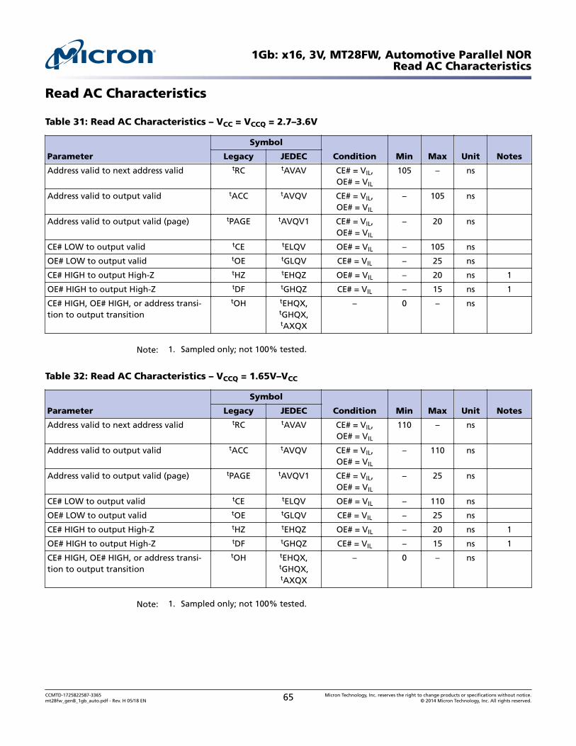
Read AC Characteristics
Table 31: Read AC Characteristics – VCC = VCCQ = 2.7–3.6V
Parameter
Symbol
Condition Min Max Unit NotesLegacy JEDEC
Address valid to next address valid tRC tAVAV CE# = VIL,OE# = VIL
105 – ns
Address valid to output valid tACC tAVQV CE# = VIL,OE# = VIL
– 105 ns
Address valid to output valid (page) tPAGE tAVQV1 CE# = VIL,OE# = VIL
– 20 ns
CE# LOW to output valid tCE tELQV OE# = VIL – 105 ns
OE# LOW to output valid tOE tGLQV CE# = VIL – 25 ns
CE# HIGH to output High-Z tHZ tEHQZ OE# = VIL – 20 ns 1
OE# HIGH to output High-Z tDF tGHQZ CE# = VIL – 15 ns 1
CE# HIGH, OE# HIGH, or address transi-tion to output transition
tOH tEHQX,tGHQX,tAXQX
– 0 – ns
Note: 1. Sampled only; not 100% tested.
Table 32: Read AC Characteristics – VCCQ = 1.65V–VCC
Parameter
Symbol
Condition Min Max Unit NotesLegacy JEDEC
Address valid to next address valid tRC tAVAV CE# = VIL,OE# = VIL
110 – ns
Address valid to output valid tACC tAVQV CE# = VIL,OE# = VIL
– 110 ns
Address valid to output valid (page) tPAGE tAVQV1 CE# = VIL,OE# = VIL
– 25 ns
CE# LOW to output valid tCE tELQV OE# = VIL – 110 ns
OE# LOW to output valid tOE tGLQV CE# = VIL – 25 ns
CE# HIGH to output High-Z tHZ tEHQZ OE# = VIL – 20 ns 1
OE# HIGH to output High-Z tDF tGHQZ CE# = VIL – 15 ns 1
CE# HIGH, OE# HIGH, or address transi-tion to output transition
tOH tEHQX,tGHQX,tAXQX
– 0 – ns
Note: 1. Sampled only; not 100% tested.
1Gb: x16, 3V, MT28FW, Automotive Parallel NORRead AC Characteristics
CCMTD-1725822587-3365mt28fw_genB_1gb_auto.pdf - Rev. H 05/18 EN 65 Micron Technology, Inc. reserves the right to change products or specifications without notice.
© 2014 Micron Technology, Inc. All rights reserved.
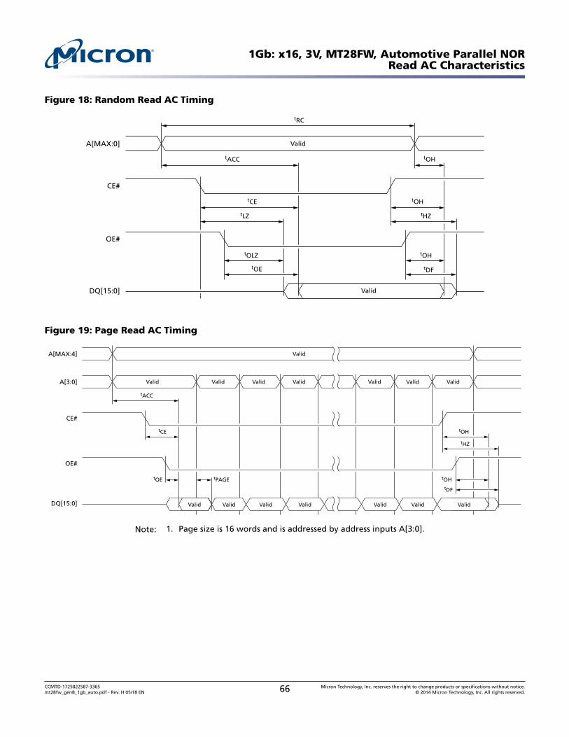
Figure 18: Random Read AC Timing
Valid
Valid
tACC
tRC
tOH
tCE
tLZ
tOH
tHZ
tOLZ tOH
tOE tDF
A[MAX:0]
CE#
OE#
DQ[15:0]
Figure 19: Page Read AC Timing
Valid
Valid Valid Valid ValidValid Valid Valid
tACC
tCE
tPAGE
tOH
tHZ
tOHtOE
tDF
A[MAX:4]
A[3:0]
CE#
OE#
DQ[15:0] Valid Valid Valid Valid Valid Valid Valid
Note: 1. Page size is 16 words and is addressed by address inputs A[3:0].
1Gb: x16, 3V, MT28FW, Automotive Parallel NORRead AC Characteristics
CCMTD-1725822587-3365mt28fw_genB_1gb_auto.pdf - Rev. H 05/18 EN 66 Micron Technology, Inc. reserves the right to change products or specifications without notice.
© 2014 Micron Technology, Inc. All rights reserved.
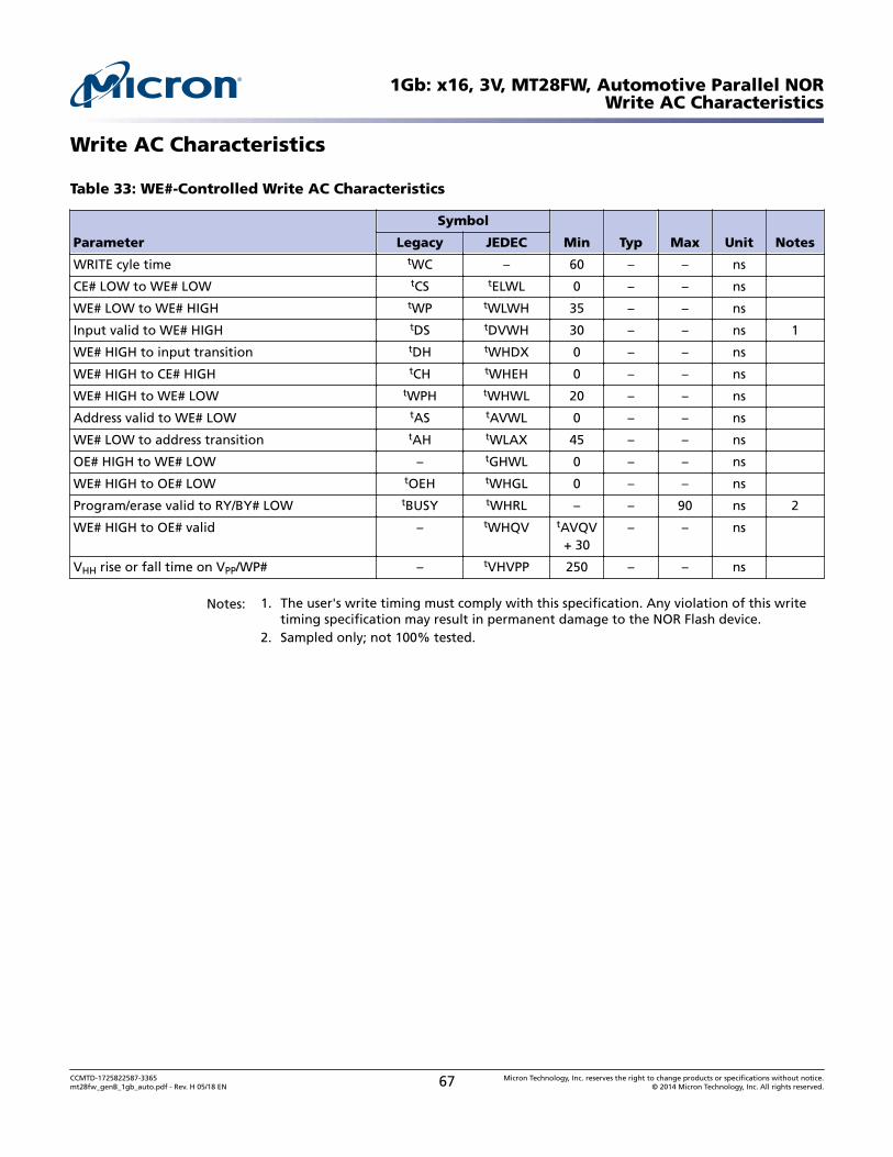
Write AC Characteristics
Table 33: WE#-Controlled Write AC Characteristics
Parameter
Symbol
Min Typ Max Unit NotesLegacy JEDEC
WRITE cyle time tWC – 60 – – ns
CE# LOW to WE# LOW tCS tELWL 0 – – ns
WE# LOW to WE# HIGH tWP tWLWH 35 – – ns
Input valid to WE# HIGH tDS tDVWH 30 – – ns 1
WE# HIGH to input transition tDH tWHDX 0 – – ns
WE# HIGH to CE# HIGH tCH tWHEH 0 – – ns
WE# HIGH to WE# LOW tWPH tWHWL 20 – – ns
Address valid to WE# LOW tAS tAVWL 0 – – ns
WE# LOW to address transition tAH tWLAX 45 – – ns
OE# HIGH to WE# LOW – tGHWL 0 – – ns
WE# HIGH to OE# LOW tOEH tWHGL 0 – – ns
Program/erase valid to RY/BY# LOW tBUSY tWHRL – – 90 ns 2
WE# HIGH to OE# valid – tWHQV tAVQV+ 30
– – ns
VHH rise or fall time on VPP/WP# – tVHVPP 250 – – ns
Notes: 1. The user's write timing must comply with this specification. Any violation of this writetiming specification may result in permanent damage to the NOR Flash device.
2. Sampled only; not 100% tested.
1Gb: x16, 3V, MT28FW, Automotive Parallel NORWrite AC Characteristics
CCMTD-1725822587-3365mt28fw_genB_1gb_auto.pdf - Rev. H 05/18 EN 67 Micron Technology, Inc. reserves the right to change products or specifications without notice.
© 2014 Micron Technology, Inc. All rights reserved.
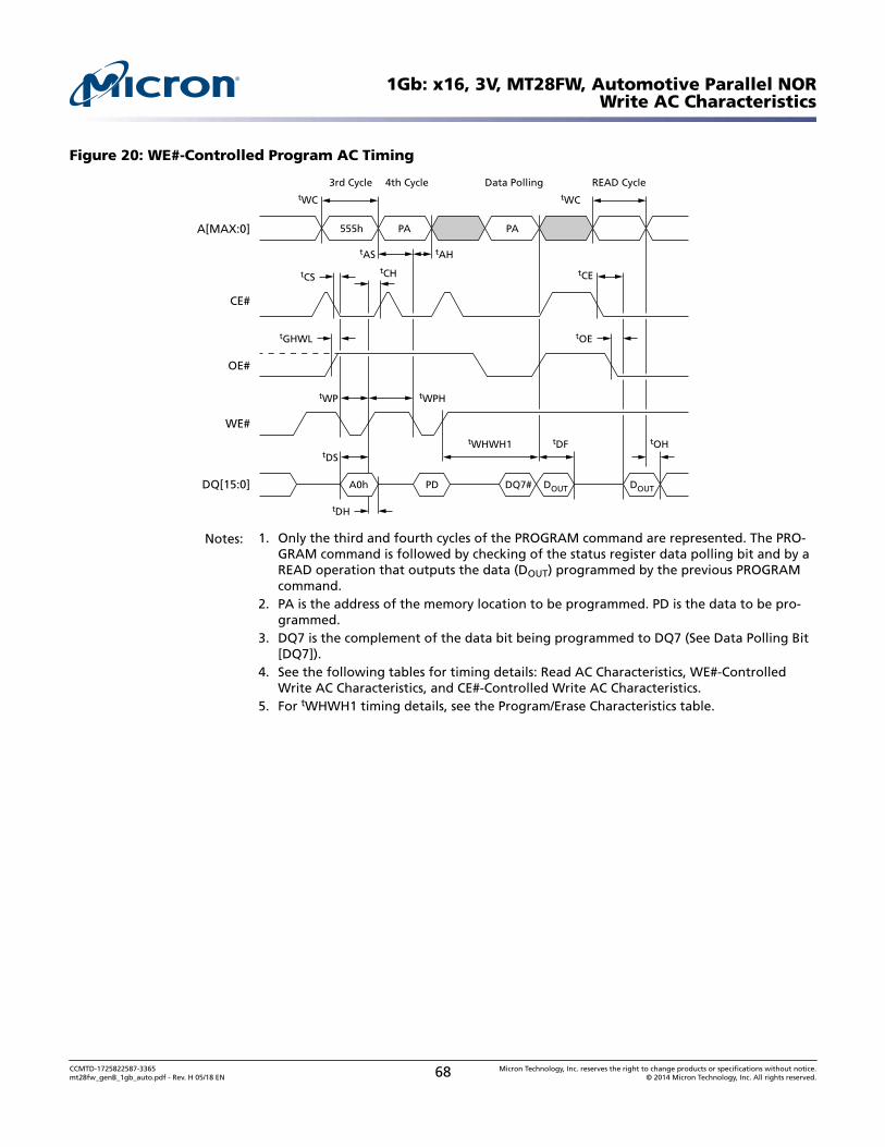
Figure 20: WE#-Controlled Program AC Timing
555h PA PA
3rd Cycle 4th Cycle READ CycleData PollingtWC tWC
tAS
tWP
tDS
tDFtWHWH1
tWPH
tAH
tCEtCS
tGHWL tOE
tDH
tOH
tCH
A[MAX:0]
CE#
OE#
WE#
DQ[15:0] A0h PD DQ7# DOUT DOUT
Notes: 1. Only the third and fourth cycles of the PROGRAM command are represented. The PRO-GRAM command is followed by checking of the status register data polling bit and by aREAD operation that outputs the data (DOUT) programmed by the previous PROGRAMcommand.
2. PA is the address of the memory location to be programmed. PD is the data to be pro-grammed.
3. DQ7 is the complement of the data bit being programmed to DQ7 (See Data Polling Bit[DQ7]).
4. See the following tables for timing details: Read AC Characteristics, WE#-ControlledWrite AC Characteristics, and CE#-Controlled Write AC Characteristics.
5. For tWHWH1 timing details, see the Program/Erase Characteristics table.
1Gb: x16, 3V, MT28FW, Automotive Parallel NORWrite AC Characteristics
CCMTD-1725822587-3365mt28fw_genB_1gb_auto.pdf - Rev. H 05/18 EN 68 Micron Technology, Inc. reserves the right to change products or specifications without notice.
© 2014 Micron Technology, Inc. All rights reserved.
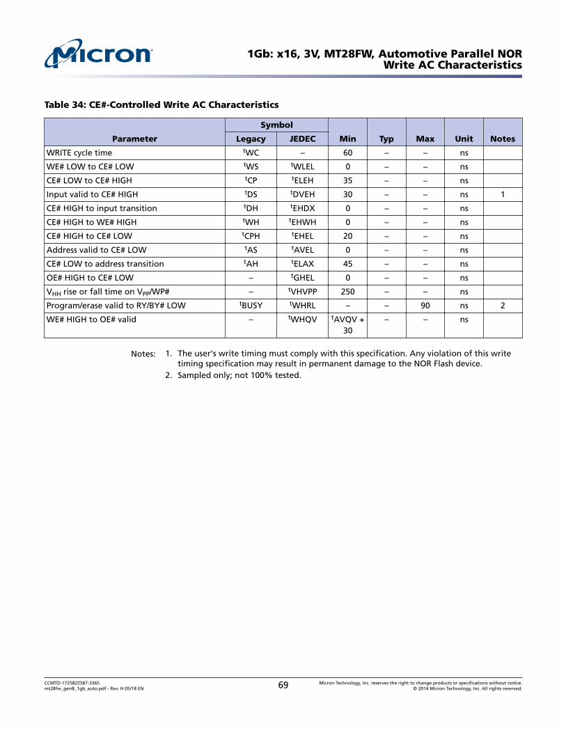
Table 34: CE#-Controlled Write AC Characteristics
Parameter
Symbol
Min Typ Max Unit NotesLegacy JEDEC
WRITE cycle time tWC – 60 – – ns
WE# LOW to CE# LOW tWS tWLEL 0 – – ns
CE# LOW to CE# HIGH tCP tELEH 35 – – ns
Input valid to CE# HIGH tDS tDVEH 30 – – ns 1
CE# HIGH to input transition tDH tEHDX 0 – – ns
CE# HIGH to WE# HIGH tWH tEHWH 0 – – ns
CE# HIGH to CE# LOW tCPH tEHEL 20 – – ns
Address valid to CE# LOW tAS tAVEL 0 – – ns
CE# LOW to address transition tAH tELAX 45 – – ns
OE# HIGH to CE# LOW – tGHEL 0 – – ns
VHH rise or fall time on VPP/WP# – tVHVPP 250 – – ns
Program/erase valid to RY/BY# LOW tBUSY tWHRL – – 90 ns 2
WE# HIGH to OE# valid – tWHQV tAVQV +30
– – ns
Notes: 1. The user's write timing must comply with this specification. Any violation of this writetiming specification may result in permanent damage to the NOR Flash device.
2. Sampled only; not 100% tested.
1Gb: x16, 3V, MT28FW, Automotive Parallel NORWrite AC Characteristics
CCMTD-1725822587-3365mt28fw_genB_1gb_auto.pdf - Rev. H 05/18 EN 69 Micron Technology, Inc. reserves the right to change products or specifications without notice.
© 2014 Micron Technology, Inc. All rights reserved.
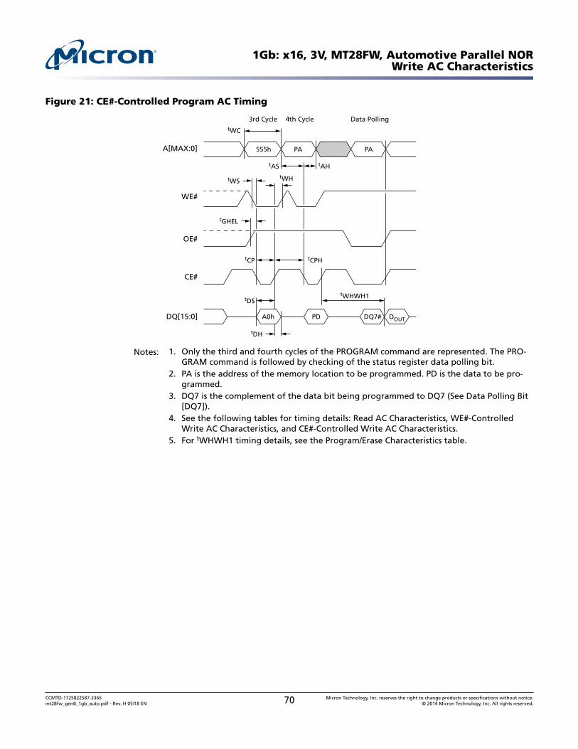
Figure 21: CE#-Controlled Program AC Timing
555h PA PA
3rd Cycle 4th Cycle Data PollingtWC
tAS
tCP
tDStWHWH1
tCPH
tAH
tWS
tGHEL
tDH
tWH
A[MAX:0]
WE#
OE#
CE#
DQ[15:0] A0h PD DQ7# DOUT
Notes: 1. Only the third and fourth cycles of the PROGRAM command are represented. The PRO-GRAM command is followed by checking of the status register data polling bit.
2. PA is the address of the memory location to be programmed. PD is the data to be pro-grammed.
3. DQ7 is the complement of the data bit being programmed to DQ7 (See Data Polling Bit[DQ7]).
4. See the following tables for timing details: Read AC Characteristics, WE#-ControlledWrite AC Characteristics, and CE#-Controlled Write AC Characteristics.
5. For tWHWH1 timing details, see the Program/Erase Characteristics table.
1Gb: x16, 3V, MT28FW, Automotive Parallel NORWrite AC Characteristics
CCMTD-1725822587-3365mt28fw_genB_1gb_auto.pdf - Rev. H 05/18 EN 70 Micron Technology, Inc. reserves the right to change products or specifications without notice.
© 2014 Micron Technology, Inc. All rights reserved.
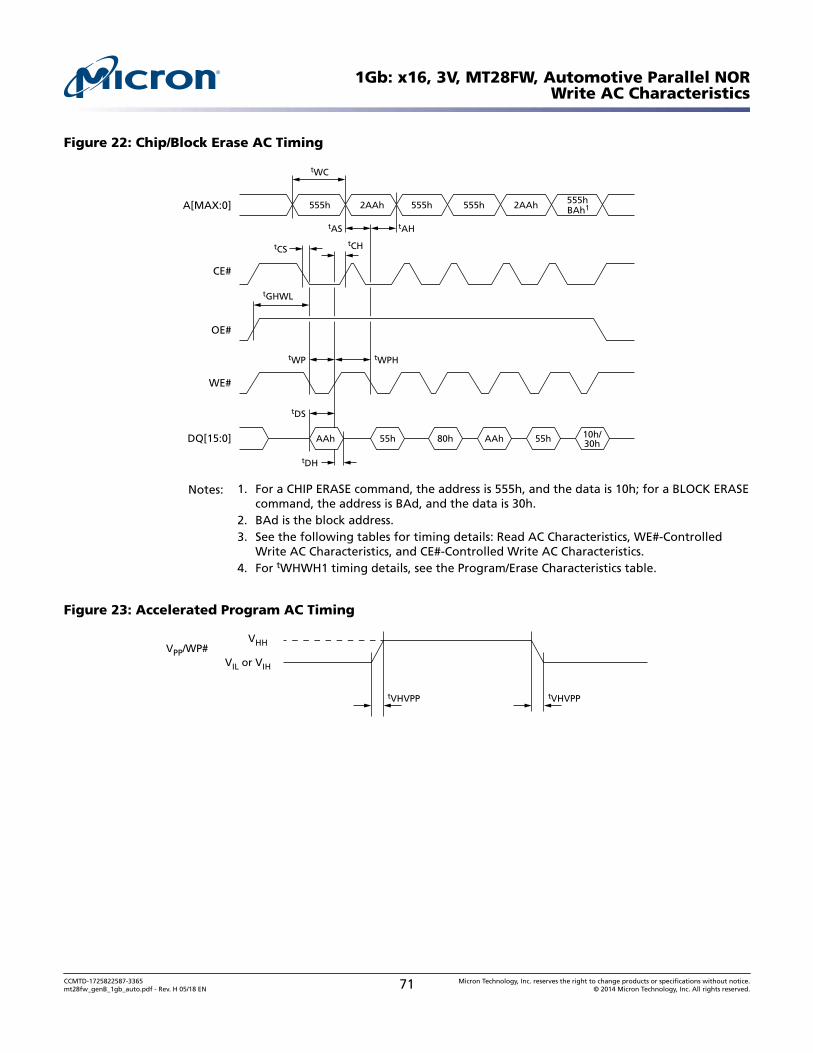
Figure 22: Chip/Block Erase AC Timing
555h
tWC
tAS
tWP
tDS
tWPH
tAH
tCS
tGHWL
tDH
tCH
A[MAX:0]
CE#
OE#
WE#
DQ[15:0] AAh
2AAh 555h 555hBAh12AAh555h
55h 55hAAh80h 10h/30h
Notes: 1. For a CHIP ERASE command, the address is 555h, and the data is 10h; for a BLOCK ERASEcommand, the address is BAd, and the data is 30h.
2. BAd is the block address.3. See the following tables for timing details: Read AC Characteristics, WE#-Controlled
Write AC Characteristics, and CE#-Controlled Write AC Characteristics.4. For tWHWH1 timing details, see the Program/Erase Characteristics table.
Figure 23: Accelerated Program AC Timing
tVHVPPtVHVPP
VHH
VIL or VIH
VPP/WP#
1Gb: x16, 3V, MT28FW, Automotive Parallel NORWrite AC Characteristics
CCMTD-1725822587-3365mt28fw_genB_1gb_auto.pdf - Rev. H 05/18 EN 71 Micron Technology, Inc. reserves the right to change products or specifications without notice.
© 2014 Micron Technology, Inc. All rights reserved.
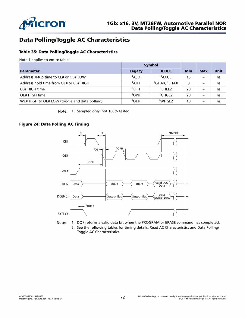
Data Polling/Toggle AC Characteristics
Table 35: Data Polling/Toggle AC Characteristics
Note 1 applies to entire table
Parameter
Symbol
Min Max UnitLegacy JEDEC
Address setup time to CE# or OE# LOW tASO tAXGL 15 – ns
Address hold time from OE# or CE# HIGH tAHT tGHAX, tEHAX 0 – ns
CE# HIGH time tEPH tEHEL2 20 – ns
OE# HIGH time tOPH tGHGL2 20 – ns
WE# HIGH to OE# LOW (toggle and data polling) tOEH tWHGL2 10 – ns
Note: 1. Sampled only; not 100% tested.
Figure 24: Data Polling AC Timing
DQ7#Data DQ7# Valid DQ7Data
Output flagData Output flag ValidDQ[6:0] Data
tHZ/tDFtCE
tOEtOPH
tCH
tBUSY
tOEH
CE#
OE#
WE#
DQ[6:0]
DQ7
RY/BY#
Notes: 1. DQ7 returns a valid data bit when the PROGRAM or ERASE command has completed.2. See the following tables for timing details: Read AC Characteristics and Data Polling/
Toggle AC Characteristics.
1Gb: x16, 3V, MT28FW, Automotive Parallel NORData Polling/Toggle AC Characteristics
CCMTD-1725822587-3365mt28fw_genB_1gb_auto.pdf - Rev. H 05/18 EN 72 Micron Technology, Inc. reserves the right to change products or specifications without notice.
© 2014 Micron Technology, Inc. All rights reserved.
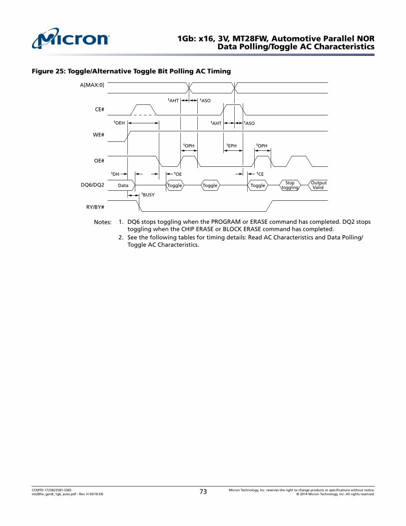
Figure 25: Toggle/Alternative Toggle Bit Polling AC Timing
Toggle Toggle ToggleData Stoptoggling
OutputValid
tBUSY
tOPH tEPH
tOEH
CE#
WE#
OE#
DQ6/DQ2
RY/BY#
tOPH
tAHT tASO
tAHT
tDH
tASO
A[MAX:0]
tOE tCE
Notes: 1. DQ6 stops toggling when the PROGRAM or ERASE command has completed. DQ2 stopstoggling when the CHIP ERASE or BLOCK ERASE command has completed.
2. See the following tables for timing details: Read AC Characteristics and Data Polling/Toggle AC Characteristics.
1Gb: x16, 3V, MT28FW, Automotive Parallel NORData Polling/Toggle AC Characteristics
CCMTD-1725822587-3365mt28fw_genB_1gb_auto.pdf - Rev. H 05/18 EN 73 Micron Technology, Inc. reserves the right to change products or specifications without notice.
© 2014 Micron Technology, Inc. All rights reserved.
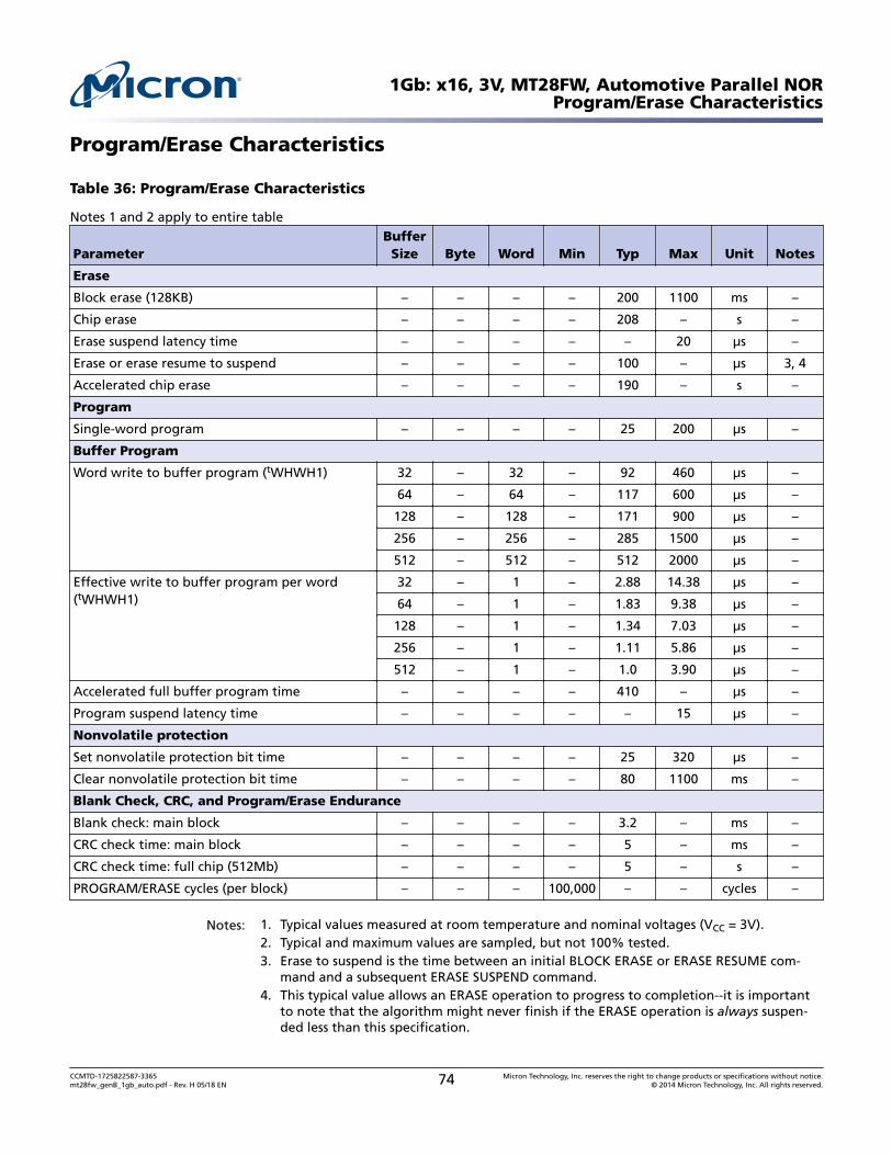
Program/Erase Characteristics
Table 36: Program/Erase Characteristics
Notes 1 and 2 apply to entire table
ParameterBufferSize Byte Word Min Typ Max Unit Notes
Erase
Block erase (128KB) – – – – 200 1100 ms –
Chip erase – – – – 208 – s –
Erase suspend latency time – – – – – 20 µs –
Erase or erase resume to suspend – – – – 100 – µs 3, 4
Accelerated chip erase – – – – 190 – s –
Program
Single-word program – – – – 25 200 µs –
Buffer Program
Word write to buffer program (tWHWH1) 32 – 32 – 92 460 µs –
64 – 64 – 117 600 µs –
128 – 128 – 171 900 µs –
256 – 256 – 285 1500 µs –
512 – 512 – 512 2000 µs –
Effective write to buffer program per word(tWHWH1)
32 – 1 – 2.88 14.38 µs –
64 – 1 – 1.83 9.38 µs –
128 – 1 – 1.34 7.03 µs –
256 – 1 – 1.11 5.86 µs –
512 – 1 – 1.0 3.90 µs –
Accelerated full buffer program time – – – – 410 – µs –
Program suspend latency time – – – – – 15 µs –
Nonvolatile protection
Set nonvolatile protection bit time – – – – 25 320 µs –
Clear nonvolatile protection bit time – – – – 80 1100 ms –
Blank Check, CRC, and Program/Erase Endurance
Blank check: main block – – – – 3.2 – ms –
CRC check time: main block – – – – 5 – ms –
CRC check time: full chip (512Mb) – – – – 5 – s –
PROGRAM/ERASE cycles (per block) – – – 100,000 – – cycles –
Notes: 1. Typical values measured at room temperature and nominal voltages (VCC = 3V).2. Typical and maximum values are sampled, but not 100% tested.3. Erase to suspend is the time between an initial BLOCK ERASE or ERASE RESUME com-
mand and a subsequent ERASE SUSPEND command.4. This typical value allows an ERASE operation to progress to completion--it is important
to note that the algorithm might never finish if the ERASE operation is always suspen-ded less than this specification.
1Gb: x16, 3V, MT28FW, Automotive Parallel NORProgram/Erase Characteristics
CCMTD-1725822587-3365mt28fw_genB_1gb_auto.pdf - Rev. H 05/18 EN 74 Micron Technology, Inc. reserves the right to change products or specifications without notice.
© 2014 Micron Technology, Inc. All rights reserved.
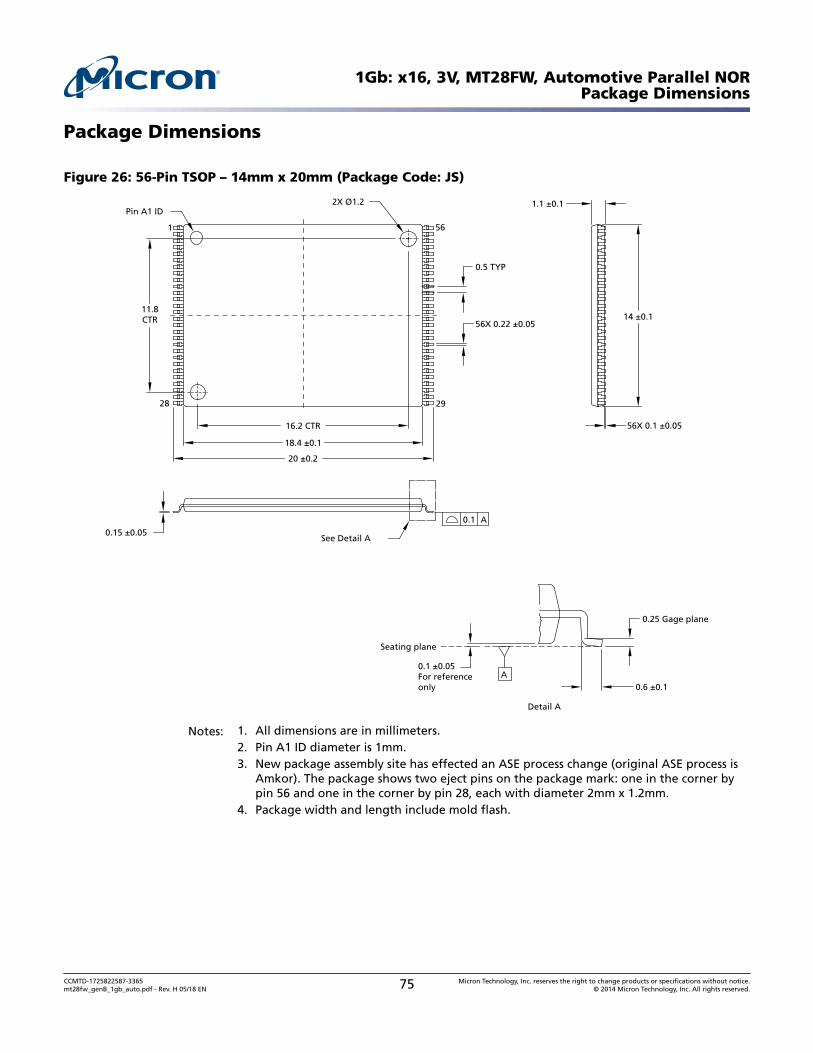
Package Dimensions
Figure 26: 56-Pin TSOP – 14mm x 20mm (Package Code: JS)
Detail A
Seating plane
0.6 ±0.1
0.25 Gage plane
0.1 ±0.05For reference only
Pin A1 ID
0.1 A
See Detail A
56X 0.1 ±0.05
0.15 ±0.05
56X 0.22 ±0.0514 ±0.1
18.4 ±0.1
20 ±0.2
1.1 ±0.1
0.5 TYP
16.2 CTR
11.8CTR
2X Ø1.2
29
561
28
A
Notes: 1. All dimensions are in millimeters.2. Pin A1 ID diameter is 1mm.3. New package assembly site has effected an ASE process change (original ASE process is
Amkor). The package shows two eject pins on the package mark: one in the corner bypin 56 and one in the corner by pin 28, each with diameter 2mm x 1.2mm.
4. Package width and length include mold flash.
1Gb: x16, 3V, MT28FW, Automotive Parallel NORPackage Dimensions
CCMTD-1725822587-3365mt28fw_genB_1gb_auto.pdf - Rev. H 05/18 EN 75 Micron Technology, Inc. reserves the right to change products or specifications without notice.
© 2014 Micron Technology, Inc. All rights reserved.
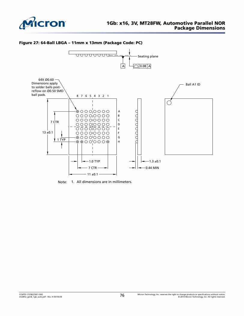
Figure 27: 64-Ball LBGA – 11mm x 13mm (Package Code: PC)
0.44 MIN
1.3 ±0.1
7 CTR
11 ±0.1
1 TYP
13 ±0.1
1.0 TYP
Ball A1 ID
Seating plane
0.08 AA
64X Ø0.60Dimensions applyto solder balls post-reflow on Ø0.50 SMDball pads.
7 CTR
A
B
C
D
E
F
G
H
234567 18
Note: 1. All dimensions are in millimeters.
1Gb: x16, 3V, MT28FW, Automotive Parallel NORPackage Dimensions
CCMTD-1725822587-3365mt28fw_genB_1gb_auto.pdf - Rev. H 05/18 EN 76 Micron Technology, Inc. reserves the right to change products or specifications without notice.
© 2014 Micron Technology, Inc. All rights reserved.
Revision History
Rev. H –05/18
• Added Important Notes and Warnings section for further clarification aligning to in-dustry standards
Rev. G – 11/16
• Updated 56-pin dimension drawing• Added Note 4 to 56-pin dimension drawing
Rev. F – 6/16
• Updated Table 21: CFI Query System Interface Information in Common Flash Inter-face
Rev. E – 9/15
• Updated Table 31: Read AC Characteristics – tPAGE in Read AC Characteristics
Rev. D – 01/15
• Promoted the document from Preliminary to Production status
Rev. C – 12/14
• Updated Figure 4: 64-Ball LBGA in Signal Assignments• Updated Table 21: CFI Query System Interface Information in Common Flash Inter-
face• Updated Table 23: Primary Algorithm-Specific Extended Query Table in Common
Flash Interface• Updated Table 28: Input/Output Capacitance in Absolute Ratings and Operating Con-
ditions• Updated Table 29: DC Current Characteristics in DC Characteristics• Updated Table 31: Read AC Characteristics – VCC = VCCQ = 2.7-3.6Vin Read AC Charac-
teristics• Updated Table 32: Read AC Characteristics – VCCQ = 1.65V - VCC in Read AC Character-
istics• Updated Table 36: Program/Erase Characteristics in Program/Erase Characteristics
Rev. B – 07/14
• Preliminary status
Rev. A – 05/14
• Initial release
1Gb: x16, 3V, MT28FW, Automotive Parallel NORRevision History
CCMTD-1725822587-3365mt28fw_genB_1gb_auto.pdf - Rev. H 05/18 EN 77 Micron Technology, Inc. reserves the right to change products or specifications without notice.
© 2014 Micron Technology, Inc. All rights reserved.
8000 S. Federal Way, P.O. Box 6, Boise, ID 83707-0006, Tel: 208-368-4000www.micron.com/products/support Sales inquiries: 800-932-4992
Micron and the Micron logo are trademarks of Micron Technology, Inc.All other trademarks are the property of their respective owners.
This data sheet contains minimum and maximum limits specified over the power supply and temperature range set forth herein.Although considered final, these specifications are subject to change, as further product development and data characterization some-
times occur.
1Gb: x16, 3V, MT28FW, Automotive Parallel NORRevision History
CCMTD-1725822587-3365mt28fw_genB_1gb_auto.pdf - Rev. H 05/18 EN 78 Micron Technology, Inc. reserves the right to change products or specifications without notice.
© 2014 Micron Technology, Inc. All rights reserved.
Related Documents