FEATURES 64Mbits organized as either 8M x 8-bits or 4M x16-bits Fast 60ns read/write access time Functionally compatible with traditional single power supply Flash devices Simultaneous read/write operations Flexible bank architecture Single 3.3V power supply Ultra low power consumption Near zero power standby operation Full HiRel temperature range (-40 o C to 105 o C) Data retention > 20 years @ +90 o C Programming Endurance: 10k cycles per sector Operational environment: - Total dose: 10 or 50 krad(Si) - SEL Immune: 80 MeV-cm 2 /mg @ 105 o C - SEU Immune: Memory Cell 102 MeV-cm 2 /mg @25 o C 48-pin ceramic flatpack package Standard Microelectronic Drawing (SMD), 5962-12204 - QML Q and Q+ INTRODUCTION The Aeroflex 64Mbit, 3.3 volt-only flash memory device, can be organized as 4,194,304 words of 16-bits each or 8,388,608 bytes of 8-bits each. Word mode data appears on DQ[15:0]; byte mode data appears on DQ[7:0]. The device is designed to be programmed in-system with the standard 3.3 volt VCC supply and can also be programmed in standard PROM programmers. The device is available with an access time of 60 ns and is offered in a 48-pin ceramic flatpack package. Standard control pins—Chip Enable (CE#), Write Enable (WE#), and Output Enable (OE#)—control normal read and write operations, and avoid bus contention issues. The device operates from a single 3.3 volt power supply. APPLICATION The UT8QNF8M8 64Mbit Flash Memory is compatible for use with the UT699 LEON 3FT microprocessor. In a typical application, the microprocessor transfers an image of the application program or kernel from non-volatile memory, such as flash, to volatile memory, such as SRAM. The Aeroflex 64Mbit NOR Flash is intended to provide customers with a non- volatile solution that has a memory capacity large enough to house a typical application program or kernel. Standard Products UT8QNF8M8 64Mbit NOR Flash Memory Datasheet May 1, 2018 www.aeroflex.com/Norflash Figure 1. UT8QNF8M8 Flash Block Diagram Bank 2 X-Decoder Bank 1 X-Decoder Bank 3 X-Decoder State Control & Command Register Y-Gate Y-Gate Bank 4 X-Decoder DQ[15:0] MUX DQ[15:0] DQ[15:0] DQ[15:0] DQ[15:0] BYTE# OE# Status Control A[21:0] A[21:0] DQ[15:0] A[21:0] RY/BY# WE# CE# RESET# WP# / ACC A[21:0] A[21:0] MUX MUX Bank 1 Address Bank 2 Address Bank 3 Address Bank 4 Address

Welcome message from author
This document is posted to help you gain knowledge. Please leave a comment to let me know what you think about it! Share it to your friends and learn new things together.
Transcript

1
FEATURES 64Mbits organized as either 8M x 8-bits or 4M x16-bits Fast 60ns read/write access time Functionally compatible with traditional single power
supply Flash devices Simultaneous read/write operations Flexible bank architecture Single 3.3V power supply Ultra low power consumption Near zero power standby operation
Full HiRel temperature range (-40oC to 105oC)
Data retention > 20 years @ +90oC Programming Endurance: 10k cycles per sector Operational environment:
- Total dose: 10 or 50 krad(Si)
- SEL Immune: 80 MeV-cm2/mg @ 105oC
- SEU Immune: Memory Cell 102 MeV-cm2/mg @25oC 48-pin ceramic flatpack package Standard Microelectronic Drawing (SMD), 5962-12204
- QML Q and Q+
INTRODUCTIONThe Aeroflex 64Mbit, 3.3 volt-only flash memory device, can be organized as 4,194,304 words of 16-bits each or 8,388,608 bytes of 8-bits each. Word mode data appears on DQ[15:0]; byte mode data appears on DQ[7:0]. The device is designed to be programmed in-system with the standard 3.3 volt VCC supply and can also be programmed in standard PROM programmers. The device is available with an access time of 60 ns and is offered in a 48-pin ceramic flatpack package. Standard control pins—Chip Enable (CE#), Write Enable (WE#), and Output Enable (OE#)—control normal read and write operations, and avoid bus contention issues. The device operates from a single 3.3 volt power supply.
APPLICATIONThe UT8QNF8M8 64Mbit Flash Memory is compatible for use with the UT699 LEON 3FT microprocessor. In a typical application, the microprocessor transfers an image of the application program or kernel from non-volatile memory, such as flash, to volatile memory, such as SRAM. The Aeroflex 64Mbit NOR Flash is intended to provide customers with a non-volatile solution that has a memory capacity large enough to house a typical application program or kernel.
Standard Products
UT8QNF8M8 64Mbit NOR Flash MemoryDatasheetMay 1, 2018www.aeroflex.com/Norflash
Figure 1. UT8QNF8M8 Flash Block Diagram
Bank 2
X-Decoder
Bank 1
X-Decoder
Bank 3
X-Decoder
State Control & Command Register
Y-G
ate
Y-G
ate
Bank 4
X-Decoder
DQ[15:0]
MUX
DQ[15:0]
DQ[15:0]
DQ[15:0]
DQ[15:0]
BYTE#OE#
Status
Control
A[21:0]
A[21:0]
DQ[15:0]
A[21:0]
RY/BY#
WE#CE#
RESET#
WP# / ACC
A[2
1:0]
A[2
1:0
]
MUX
MUX
Bank 1 Address
Bank 2 Address
Bank 3 Address
Bank 4 Address

2
1
2
3
4
5
7
6
48
47
46
45
44
42
43
A15
A14
A13
A12
A11
A10
A9
A16
BYTE#
VSS
DQ15/A-1
DQ7
DQ6
8 41A8 DQ13
DQ14
9 40A19 DQ5
10 39A20 DQ12
48-Lead Flatpack
Top View
WE#
RESET#
A21
WP#
RY/BY#
A18
A17
A7
A6
A5
11
12
13
14
15
17
16
18
19
20
A4
A3
A2
A1
21
22
23
24
38
37
36
35
34
32
33
DQ4
VCC
DQ11
DQ3
DQ10
DQ9
31 DQ1
DQ2
30 DQ8
29 DQ028 OE#
27 VSS
26 CE#
25 A0
Figure 2. UT8QNF8M8 Pinout (48)
Table 1. Pin Descriptions
SIGNAL FUNCTION
A[21:0] 22 Address pins
DQ[14:0] 15 Data Inputs/Outputs, (x16-mode only)
DQ15/A-1 DQ15 (Data Input/Output, word mode), A-1 (LSB Address Input, byte mode)
CE# Chip Enable, Active Low
OE# Output Enable, Active Low
WE# Write Enable, Active Low
WP# Hardware Write Protect
RESET# Hardware reset pin, Active Low
BYTE# Select 8-bit or 16-bit mode, Active Low
RY/BY# Ready/Busy Output, Active Low
VCC 3.3 volt only single power supply (see supply tolerances)
VSS Device Ground

3
SIMULTANEOUS READ/WRITE OPERATIONS WITH ZERO LATENCY
The Simultaneous Read/Write architecture provides simultane-ous operation by dividing the memory space into four banks, two 8 Mb banks with small and large sectors, and two 24 Mb banks of large sectors. Sector addresses are fixed, system software can be used to form user-defined bank groups.
During an Erase/Program operation, any of the three non-busy banks may be read from. Note that only two banks can operate
simultaneously. The device can improve overall system perfor-mance by allowing a host system to program or erase in one bank, then immediately and simultaneously read from the other bank, with zero latency. This releases the system from waiting for the completion of program or erase operations.
The UT8QNF8M8 is organized as a dual boot device with both top and bottom boot sectors.
Table 2. Bank Architecture
Bank 1 8 Mb Eight 8 kbyte/4 kword,Fifteen 64 kybte/32 word
Bank 2 24 Mb Forty-eight 64 kbyte/32 kword
Bank 3 24 Mb Forty-eight 64 kbyte/32 kword
Bank 4 8 Mb Eight 8 kbyte/4 kword,Fifteen 64 kbyte/32 kword

4
UT8QNF8M8 FEATURESThe device offers complete compatibility with the JEDEC 42.4 single-power-supply Flash command set standard. Commands are written to the command register using standard micropro-cessor write timings. Reading data out of the device is similar to reading from other Flash or EPROM devices.
The host system can detect whether a program or erase opera-tion is complete by using the device status bits: RY/BY# pin, DQ7 (Data# Polling) and DQ6/DQ2 (toggle bits). After a pro-gram or erase cycle has been completed, the device automati-cally returns to the read mode.
The sector erase architecture allows memory sectors to be erased and reprogrammed without affecting the data contents of other sectors. The device is fully erased when shipped from the factory.
Hardware data protection measures include a low VCC detector that automatically inhibits write operations during power tran-sitions. The hardware sector protection feature disables both program and erase operations in sectors 0, 1, 140, and 141.
The Erase Suspend/Erase Resume feature enables the user to put erase on hold for any period of time to read data from, or program data to, any sector that is not selected for erasure. True background erase can thus be achieved.
The device offers two power-saving features. When addresses have been stable for a specified amount of time, the device en-ters the automatic sleep mode. The system can also place the device into the standby mode. Power consumption is greatly re-duced in both modes.

5
DEVICE BUS OPERATION
This section describes the requirements and use of the device bus operations, which are initiated through the internal command register. The command register itself does not occupy any addressable memory location. The register is a latch used to store the commands, along with the address and
data information needed to execute the command. The contents of the register serve as inputs to the internal state machine. The state machine outputs dictate the function of the device. Table 3 lists the device bus operations, the inputs and control levels they require, and the resulting output.
Table 3. UT8QNF8M8 Device Bus Operations
OPERATION CE# OE# WE# RESET# WP# Addresses1
DQ[15:8]
BYTE# = VIH
BYTE# = VIL DQ[7:0]
Read L L H H L/H AIN DOUT DQ[14:8] = High-Z,DQ15 = A-1
DOUT
Write L H L H (Note 2) AIN DIN DIN
Standby VCC + 0.3V
X X VCC + 0.3V
L/H X High-Z High-Z High-Z
Output Disable L H H H L/H X High-Z High-Z High-Z
Reset X X X L L/H X High-Z High-Z High-Z
Notes:1. Addresses are A21:A0 in word mode (BYTE# = VIH), A21:A-1 in byte mode (BYTE# = VIL).2. If WP# = VIL, sectors 0, 1, 140, and 141 remain protected.

6
Word/Byte ConfigurationThe BYTE# pin controls whether the device data I/O pins operate in the byte or word configuration. If the BYTE# pin is set at logic 1, the device is in word configuration, DQ[15:0] are active and controlled by CE# and OE#.
If the BYTE# pin is set at logic ‘0’, the device is in byte configuration, and only data I/O pins [DQ7:0] are active and controlled by CE# and OE#. The data I/O pins [DQ14:8] are tri-stated, and the DQ15 pin is used as an input for the LSB (A-1) address function. The BYTE# pin must be connected to either the system VCC or ground.
Requirements for Reading Array DataTo read array data from the outputs, the system must drive the CE# and OE# pins to VIL. CE# is the power control and selects
the device. OE# is the output control and gates array data to the output pins. WE# should remain at VIH. The BYTE# pin
determines whether the device outputs array data in words or bytes.
The internal state machine is set for reading array data upon device power-up or after a hardware reset. This ensures that no spurious alteration of the memory content occurs during the power transition. No command is necessary in this mode to obtain array data. Standard microprocessor read cycles that assert valid addresses on the device address inputs produce valid data on the device data outputs. Each bank remains enabled forread access until the command register contents are altered.
Refer to Read-Only Operations for timing specifications and to Figure 7 for the timing diagram. ICC1 represents the active
current specification for reading array data.
Writing Commands/Command SequencesTo write a command or command sequence (which includes programming data to the device and erasing sectors of memory), the system must drive WE# and CE# to VIL, and OE# to VIH.
For program operations, the BYTE# pin determines whether the device accepts program data in bytes or words. Refer to Word/Byte Configuration.
The device features an Unlock Bypass mode to facilitate faster programming. Once a bank enters the Unlock Bypass mode, only two write cycles are required to program a word or byte, instead of four. Byte/ Word Program Command Sequence has details on programming data to the device using both standard and Unlock Bypass command sequences.
An erase operation can erase one sector, multiple sectors, or the entire device. Table 4 indicates the address space that each sector occupies. Similarly, a sector address is the address bits required to uniquely select a sector. Command Definitions section has details on erasing a sector or the entire chip, or suspending/resuming the erase operation.
The device address space is divided into four banks. A bank address is the address bits required to uniquelyselect a bank.
ICC2 represents the active current specification for the write
mode. AC Characteristics section contains timing specification tables and timing diagrams for write operations.
Autoselect FunctionsIf the system writes the autoselect command sequence, the device enters the autoselect mode. The system can then read autoselect codes from the internal register which is separate from the memory array on [DQ15:0]. Standard read cycle timings apply in this mode. Refer to the Autoselect Command Sequence section for more information.
Simultaneous Read/Write Operations with Zero LatencyThis device is capable of reading data from one bank of memory while programming or erasing in another bank of memory. An erase operation may also be suspended to read from or program to another location within the same bank except the sector being erased. Figure 13 shows how read and write cycles may be initiated for simultaneous operation with zero latency.
Standby ModeWhen the system is not reading or writing to the device, it can place the device in the standby mode. In this mode, current con-sumption is greatly reduced, and the outputs are placed in the high impedance state, independent of the OE# input.
The device enters the CMOS standby mode when the CE# and RESET# pins are both held at VCC ± 0.3V. This is a more re-stricted voltage range than VIH. If CE# and RESET# are held at VIH, but not within VCC ± 0.3V, the device will be in the stand-by mode, but the standby current will be greater. The device re-quires standard access time (tCE) for read access when the device is in either of these standby modes, before it is ready to read data.
If the device is deselected during erasure or programming, the device draws active current until the operation is completed.
ICC3 represents the standby current specification.

7
Automatic Sleep ModeThe automatic sleep mode minimizes Flash device energy con-sumption. The device automatically enables this mode when ad-dresses remain stable for tACC + 30 ns. The automatic sleep mode is independent of the CE#, WE#, and OE# control signals. Standard address access timings provide new data when address-es are changed. While in sleep mode, output data is latched and always available to the system. ICC5 represents the automatic sleep mode current specification.
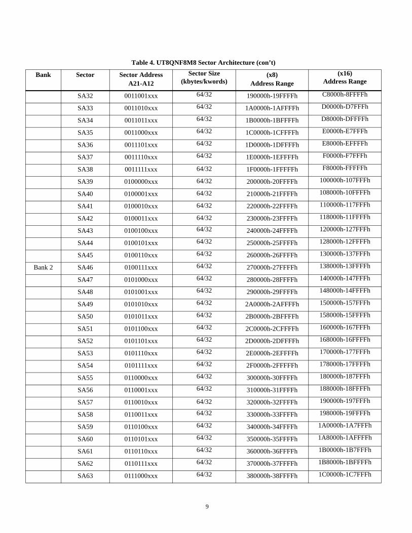
RESET#: Hardware Reset PinThe RESET# pin provides a hardware method of resetting the device to reading array data. When the RESET# pin is driven low for at least a period of tRP, the device immediately termi-nates any operation in progress, tristates all output pins, and ig-nores all read/write commands for the duration of the RESET# pulse. The device also resets the internal state machine to read-ing array data. The operation that was interrupted should be reinitiated once the device is ready to accept another command sequence to ensure data integrity.
Current is reduced for the duration of the RESET# pulse. When RESET# is held at VSS ±0.3V, the device draws CMOS standby current (ICC4). If RESET# is held at VIL but not within VSS ±0.3V, the standby current will be greater.
The RESET# pin may be tied to the system reset circuitry. A sys-tem reset would thus also reset the Flash memory, enabling the system to read the boot-up firmware from the Flash memory. The CE# pin should only go to VIL after RESET# has gone to VIH. Keeping CE# at VIL from power up through the first read could cause the first read to retrieve erroneous data.
If RESET# is asserted during a program or erase operation, the RY/BY# pin remains a logic 0 (busy) until the internal reset op-eration is complete, which requires a time of tREADY (during Embedded Algorithms). The system can thus monitor RY/BY# to determine whether the reset operation is complete. If RESET# is asserted when a program or erase operation is not executing (RY/BY# pin is logic 1), the reset operation is completed within a time of tREADY (not during Embedded Algorithms). The sys-tem can read data tRH after the RESET# pin returns to VIH. Re-fer to Hardware Reset section for reset# parameters and to Figure 8 for the timing diagram.
Output Disable ModeWhen the OE# input is at VIH, output from the device is dis-abled. The output pins are placed in the high impedance state.

8
Table 4. UT8QNF8M8 Sector Architecture
Bank Sector Sector AddressA21-A12
Sector Size(kbytes/kwords)
(x8)Address Range
(x16)Address Range
SA0 000000000 8/4 000000h-001FFFh 00000h-00FFFh
SA1 000000001 8/4 002000h-003FFFh 01000h-01FFFh
SA2 000000010 8/4 004000h-005FFFh 02000h-02FFFh
SA3 000000011 8/4 006000h-007FFFh 03000h-03FFFh
SA4 000000100 8/4 008000h-009FFFh 04000h-04FFFh
SA5 000000101 8/4 00A000h-00BFFFh 05000h-05FFFh
SA6 000000110 8/4 00C000h-00DFFFh 06000h-06FFFh
SA7 000000111 8/4 00E000h-00FFFFh 07000h-07FFFh
SA8 000001xxx 64/32 010000h-01FFFFh 08000h-08FFFh
SA9 000010xxx 64/32 020000h-02FFFFh 10000h-17FFFh
SA10 000011xxx 64/32 030000h-03FFFFh 18000h-1FFFFh
Bank 1 SA11 000100xxx 64/32 040000h-04FFFFh 20000h-27FFFh
SA12 000101xxx 64/32 050000h-05FFFFh 28000h-2FFFFh
SA13 000110xxx 64/32 060000h-06FFFFh 30000h-37FFFh
SA14 000111xxx 64/32 070000h-07FFFFh 38000h-3FFFFh
SA15 001000xxx 64/32 080000h-08FFFFh 40000h-47FFFh
SA16 001001xxx 64/32 090000h-09FFFFh 48000h-4FFFFh
SA17 001010xxx 64/32 0A0000h-0AFFFFh 50000h-57FFFh
SA18 001011xxx 64/32 0B0000h-0BFFFFh 58000h-5FFFFh
SA19 001100xxx 64/32 0C0000h-0CFFFFh 60000h-67FFFh
SA20 001101xxx 64/32 0D0000h-0DFFFFh 68000h-6FFFFh
SA21 001110xxx 64/32 0E0000h-0EFFFFh 70000h-77FFFh
SA22 001111xxx 64/32 0F0000h-0FFFFFh 78000h-7FFFFh
SA23 0010000xxx 64/32 100000h-10FFFFh 80000h-87FFFFh
SA24 0010001xxx 64/32 110000h-11FFFFh 880000h-8FFFFh
SA25 0010010xxx 64/32 120000h-12FFFFh 90000h-97FFFh
SA26 0010011xxx 64/32 130000h-13FFFFh 980000h-9FFFFh
SA27 0010100xxx 64/32 140000h-14FFFFh A0000h-A7FFFh
SA28 0010101xxx 64/32 150000h-15FFFFh A8000h-AFFFFh
SA29 0010110xxx 64/32 160000h-16FFFFh B0000h-B7FFFh
SA30 0010111xxx 64/32 170000h-17FFFFh B8000h-BFFFFh
SA31 0011000xxx 64/32 180000h-18FFFFh C0000h-C7FFFh
9
Table 4. UT8QNF8M8 Sector Architecture (con’t)
Bank Sector Sector AddressA21-A12
Sector Size(kbytes/kwords)
(x8)Address Range
(x16)Address Range
SA32 0011001xxx 64/32 190000h-19FFFFh C8000h-8FFFFh
SA33 0011010xxx 64/32 1A0000h-1AFFFFh D0000h-D7FFFh
SA34 0011011xxx 64/32 1B0000h-1BFFFFh D8000h-DFFFFh
SA35 0011000xxx 64/32 1C0000h-1CFFFFh E0000h-E7FFFh
SA36 0011101xxx 64/32 1D0000h-1DFFFFh E8000h-EFFFFh
SA37 0011110xxx 64/32 1E0000h-1EFFFFh F0000h-F7FFFh
SA38 0011111xxx 64/32 1F0000h-1FFFFFh F8000h-FFFFFh
SA39 0100000xxx 64/32 200000h-20FFFFh 100000h-107FFFh
SA40 0100001xxx 64/32 210000h-21FFFFh 108000h-10FFFFh
SA41 0100010xxx 64/32 220000h-22FFFFh 110000h-117FFFh
SA42 0100011xxx 64/32 230000h-23FFFFh 118000h-11FFFFh
SA43 0100100xxx 64/32 240000h-24FFFFh 120000h-127FFFh
SA44 0100101xxx 64/32 250000h-25FFFFh 128000h-12FFFFh
SA45 0100110xxx 64/32 260000h-26FFFFh 130000h-137FFFh
Bank 2 SA46 0100111xxx 64/32 270000h-27FFFFh 138000h-13FFFFh
SA47 0101000xxx 64/32 280000h-28FFFFh 140000h-147FFFh
SA48 0101001xxx 64/32 290000h-29FFFFh 148000h-14FFFFh
SA49 0101010xxx 64/32 2A0000h-2AFFFFh 150000h-157FFFh
SA50 0101011xxx 64/32 2B0000h-2BFFFFh 158000h-15FFFFh
SA51 0101100xxx 64/32 2C0000h-2CFFFFh 160000h-167FFFh
SA52 0101101xxx 64/32 2D0000h-2DFFFFh 168000h-16FFFFh
SA53 0101110xxx 64/32 2E0000h-2EFFFFh 170000h-177FFFh
SA54 0101111xxx 64/32 2F0000h-2FFFFFh 178000h-17FFFFh
SA55 0110000xxx 64/32 300000h-30FFFFh 180000h-187FFFh
SA56 0110001xxx 64/32 310000h-31FFFFh 188000h-18FFFFh
SA57 0110010xxx 64/32 320000h-32FFFFh 190000h-197FFFh
SA58 0110011xxx 64/32 330000h-33FFFFh 198000h-19FFFFh
SA59 0110100xxx 64/32 340000h-34FFFFh 1A0000h-1A7FFFh
SA60 0110101xxx 64/32 350000h-35FFFFh 1A8000h-1AFFFFh
SA61 0110110xxx 64/32 360000h-36FFFFh 1B0000h-1B7FFFh
SA62 0110111xxx 64/32 370000h-37FFFFh 1B8000h-1BFFFFh
SA63 0111000xxx 64/32 380000h-38FFFFh 1C0000h-1C7FFFh

10
Bank Sector Sector AddressA21-A12
Sector Size(kbytes/kwords)
(x8)Address Range
(x16)Address Range
SA64 0111001xxx 64/32 390000h-39FFFFh 1C8000h-1CFFFFh
SA65 0111010xxx 64/32 3A0000h-3AFFFFh 1D0000h-1D7FFFh
SA66 0111011xxx 64/32 3B0000h-3BFFFFh 1D8000h-1DFFFFh
SA67 0111100xxx 64/32 3C0000h-3CFFFFh 1E0000h-1E7FFFh
SA68 0111101xxx 64/32 3D0000h-3DFFFFh 1E8000h-1EFFFFh
SA69 0111110xxx 64/32 3E0000h-3EFFFFh 1F0000h-1F7FFFh
SA70 0111111xxx 64/32 3F0000h-3FFFFFh 1F8000h-1FFFFFh
SA71 1000000xxx 64/32 400000h-40FFFFh 200000h-207FFFh
SA72 1000001xxx 64/32 410000h-41FFFFh 208000h-20FFFFh
SA73 1000010xxx 64/32 420000h-42FFFFh 210000h-217FFFh
SA74 1000011xxx 64/32 430000h-43FFFFh 218000h-21FFFFh
SA75 1000100xxx 64/32 440000h-44FFFFh 220000h-227FFFh
SA76 1000101xxx 64/32 450000h-45FFFFh 228000h-22FFFFh
SA77 1000110xxx 64/32 460000h-46FFFFh 230000h-237FFFh
SA78 1000111xxx 64/32 470000h-47FFFFh 238000h-23FFFFh
SA79 1001000xxx 64/32 480000h-48FFFFh 240000h-247FFFh
SA80 1001001xxx 64/32 490000h-49FFFFh 248000h-24FFFFh
SA81 1001010xxx 64/32 4A0000h-4AFFFFh 250000h-257FFFh
SA82 1001011xxx 64/32 4B0000h-4BFFFFh 258000h-25FFFFh
SA83 1001100xxx 64/32 4C0000h-4CFFFFh 260000h-267FFFh
SA84 1001101xxx 64/32 4D0000h-4DFFFFh 268000h-26FFFFh
SA85 1001110xxx 64/32 4E0000h-4EFFFFh 270000h-277FFFh
SA86 1001111xxx 64/32 4F0000h-4FFFFFh 278000h-27FFFFh
SA87 1010000xxx 64/32 500000h-50FFFFh 280000h-28FFFFh
SA88 1010001xxx 64/32 510000h-51FFFFh 288000h-28FFFFh
SA89 1010010xxx 64/32 520000h-52FFFFh 290000h-297FFFh
SA90 1010011xxx 64/32 530000h-53FFFFh 298000h-29FFFFh
SA91 1010100xxx 64/32 540000h-54FFFFh 2A0000h-2A7FFFh
SA92 1010101xxx 64/32 550000h-55FFFFh 2A8000h-2AFFFFh
SA93 1010110xxx 64/32 560000h-56FFFFh 2B0000h-2B7FFFh
Bank 3 SA94 1010111xxx 64/32 570000h-57FFFFh 2B8000h-2BFFFFh
SA95 1011000xxx 64/32 580000h-58FFFFh 2C0000h-2C7FFFh
SA96 1011001xxx 64/32 590000h-59FFFFh 2C8000h-2CFFFFh
Table 4. UT8QNF8M8 Sector Architecture (con’t)

11
Table 4. UT8QNF8M8 Sector Architecture (con’t)
Bank Sector Sector AddressA21-A12
Sector Size(kbytes/kwords)
(x8)Address Range
(x16)Address Range
SA97 1011010xxx 64/32 5A0000h-5AFFFFh 2D0000h-2D7FFFh
SA98 1010101xxx 64/32 5B0000h-5BFFFFh 2D8000h-2DFFFFh
SA99 1011100xxx 64/32 5C0000h-5CFFFFh 2E0000h-2E7FFFh
SA100 1011101xxx 64/32 5D0000h-5DFFFFh 2E8000h-2EFFFFh
SA101 1011110xxx 64/32 5E0000h-5EFFFFh 2F0000h-2F7FFFh
SA102 1011111xxx 64/32 5F0000h-5FFFFFh 2F8000h-2FFFFFh
SA103 1100000xxx 64/32 600000h-60FFFFh 300000h-307FFFh
SA104 1100001xxx 64/32 610000h-61FFFFh 308000h-30FFFFh
SA105 1100010xxx 64/32 620000h-62FFFFh 310000h-317FFFh
SA106 1100011xxx 64/32 630000h-63FFFFh 318000h-31FFFFh
SA107 1100100xxx 64/32 640000h-64FFFFh 320000h-327FFFh
SA108 1100101xxx 64/32 650000h-65FFFFh 328000h-32FFFFh
SA109 1100110xxx 64/32 660000h-66FFFFh 330000h-337FFFh
SA110 1101111xxx 64/32 670000h-67FFFFh 338000h-33FFFFh
SA111 1101000xxx 64/32 680000h-68FFFFh 34000h-347FFFh
SA112 1011101xxx 64/32 690000h-69FFFFh 348000h-34FFFFh
SA113 1101010xxx 64/32 6A0000h-6AFFFFh 350000h-357FFFh
SA114 1101011xxx 64/32 6B0000h-6BFFFFh 358000h-35FFFFh
SA115 1101100xxx 64/32 6C0000h-6CFFFFh 36000h-367FFFh
SA116 1101101xxx 64/32 6D0000h-6DFFFFh 368000h-36FFFFh
SA117 1101110xxx 64/32 6E0000h-6EFFFFh 37000h-377FFFh
SA118 1101111xxx 64/32 6F0000h-6FFFFFh 37800h-37FFFFh
SA119 1110000xxx 64/32 700000h-70FFFFh 380000h-387FFFh
SA120 1110001xxx 64/32 710000h-71FFFFh 388000h-38FFFFh
SA121 1110010xxx 64/32 720000h-72FFFFh 390000h-397FFFh
SA122 1110011xxx 64/32 730000h-73FFFFh 39800h-39FFFFh
SA123 1110100xxx 64/32 740000h-74FFFFh 3A0000h-3A7FFFh
SA124 1110101xxx 64/32 750000h-75FFFFh 3A8000h-3AFFFFh
SA125 1110110xxx 64/32 760000h-76FFFFh 3B0000h-3B7FFFh
SA126 1110111xxx 64/32 770000h-77FFFFh 3B8000h-3BFFFFh
SA127 1111000xxx 64/32 780000h-78FFFFh 3C0000h-3C7FFFh
SA128 1111001xxx 64/32 790000h-79FFFFh 3C8000h-3CFFFFh

12
Write Protect (WP#)The Write Protect function provides a hardware method of protecting. If the system asserts VIL on the WP# pin, the
device disables program and erase functions in sectors 0, 1, 140, and 141. WP# pin must not be left floating or uncon-nected; inconsistent behavior of the device may result.
Table 4. UT8QNF8M8 Sector Architecture con’t
Bank Sector Sector AddressA21-A12
Sector Size(kbytes/kwords)
(x8)Address Range
(x16)Address Range
SA129 1111010xxx 64/32 7A0000h-7AFFFFh 3D0000h-3D7FFFh
Bank 4 SA130 1110101xxx 64/32 7B0000h-7BFFFFh 3D8000h-3DFFFFh
SA131 1111100xxx 64/32 7C0000h-7CFFFFh 3E80000h-3E7FFFh
SA132 1111110xxx 64/32 7D0000h-7DFFFFh 3E8000h-3EFFFFh
SA133 1111110xxx 64/32 7E0000h-7EFFFFh 3F0000h-3F7FFFh
SA134 1111111000 8/4 7F0000h-7F1FFFh 3F8000h-3F8FFFh
SA135 1111111001 8/4 7F2000h-7F3FFFh 3F9000h-3F9FFFh
SA136 1111111010 8/4 7F4000h-7F5FFFh 3FA000h-3FAFFFh
SA137 1111111011 8/4 7F6000h-7F7FFFh 3FB000h-3FBFFFh
SA138 1111111100 8/4 7F8000h-7F9FFFh 3FC000h-3FCFFFh
SA139 1111111101 8/4 7FA000h-7FBFFFh 3FD000h-3FDFFFh
SA140 1111111110 8/4 7FC000h-7FDFFFh 3FE000h-3FEFFFh
SA141 1111111111 8/4 7FE000h-7FFFFFh 3FF000h-3FFFFFh
Table 5. Bank Address
Bank A21-A19
1 000
2 001, 010, 011
3 100, 101, 110
4 111
Table 6. WP# Modes
VIL Disables programming and erasing in SA0,SA1, SA140, SA141
VIH Enables programming and erasing in SA0, SA1, SA140, SA141.

13
Hardware Data ProtectionThe command sequence requirement of unlock cycles for pro-gramming or erasing provides data protection against inadver-tent writes. Refer to Table 11 for command definitions. Inaddition, the following hardware data protection measures pre-vent accidental erasure or programming, which might otherwisebe caused by spurious system level signals during VCC power-up and power-down transitions or from system noise.
Low VCC Write InhibitWhen VCC is less than VLKO, the device does not accept anywrite cycles. This protects data during VCC power-up and pow-er-down. The command register and all internal program/erasecircuits are disabled and the device resets to the read mode. Sub-sequent writes are ignored until VCC is greater than VLKO. Thesystem must provide the proper signals to the control pins to pre-vent unintentional writes when VCC is greater than VLKO.
Logical InhibitWrite cycles are inhibited by holding any one of OE# = VIL,CE# = VIH or WE# = VIH. To initiate a write cycle, CE# andWE# must be a logical zero while OE# is a logical one.
Power-Up Write InhibitIf WE# = CE# = VIL and OE# = VIH during power up, thedevice does not accept commands on the rising edge of WE#.The internal state machine is automatically reset to the read
COMMON FLASH MEMORY INTERFACE (CFI)The Common Flash Interface (CFI) specification outlines device and host system software interrogation handshake, which allows specific vendor-specified software algorithms to be used for entire families of devices. Software support can then be device-independent, JEDEC ID-independent, and forward- and backward-compatible for the specified flash device fami-lies. Flash vendors can standardize their existing interfaces for long-term compatibility.
This device enters the CFI Query mode when the system writes the CFI Query command, 98h, to address 55h in word mode (or address AAh in byte mode), any time the device is ready to read array data. The system can read CFI information at the addresses given in Table 7 to Table 10. To terminate reading CFI data, the system must write the reset command.The CFI Query mode is not accessible when the device is executing an Embedded Program or embedded Erase algorithm.
The system can also write the CFI query command when the de-vice is in the autoselect mode via the command register only(high voltage method does not apply). The device enters the CFIquery mode, and the system can read CFI data at the addressesgiven in Table 7 to Table 10. The system must write the resetcommand to return to reading array data.
mode on power-up
Table 7. CFI Query Identification String
Addresses(word mode)
Addresses(byte mode)
Data Description
10h11h12h
20h22h24h
0051h0052h0059h
Query unique ASII string "QRY"
13h14h
26h28h
002h000h
Primary OEM command set
15h16h
2Ah2Ch
0040h0000h
Address for primary extended table
17h18h
2Eh30h
000h000h
Alternate OEM command set (00h = none exists
19h1Ah
32h34h
000h000h
Address for alternate OEM extended table (00h = none exists

14
Table 8. System Interface String
Addresses(word mode)
Addresses(byte mode)
Data Description
1Bh 36h 0027h VCC min (write/erase)D7-D4: volt, D3-D0:100 millivolt
1Ch 38h 0036h VCC max (write/erase)D7-D4: volt, D3-D0:100 millivolt
1Dh 3Ah 0000h VPP min, voltage (00h=no VPP pin present)
1Eh 3Ch 0000h VPP max, voltage (00h=no VPP pin present)
1Fh 3Eh 0003h Typical timeout per single byte/word write 2N s
20h 40h 0000h Typical timeout per min. size buffer write 2N s (00h = not supported)
21h 42h 0009h Typical timeout per individual block erase 2N ms
22h 44h 000Fh Typical timeout per full chip erase 2N ms (00h = not supported)
23h 46h 0004h Max timeout for byte/word 2N times typical
24h 48h 0000h Max timeout per buffer write 2N times typical
25h 4Ah 0004h Max timeout per individual block erase 2N times typ-ical
26h 4Ch 0000h Max timeout for full chip erase 2N times typical sup-port (00h = not supported)
Table 9. Device Geometry Definition
Addresses(word mode)
Addresses(byte mode)
Data Description
27h 4Eh 0017h Device size = 2N byte
28h29h
50h52h
0002h0000h
Flash device interface description
2Ah2Bh
54h56h
0000h0000h
Max number of byte in multi-byte write = 2N (00h = not supported)
2Ch 58h 0003h Number of erase block regions within device
2Dh2Eh2Fh30h
5Ah5Ch5Eh60h
0007h0000h0020h0000H
Erase block region 1 information
31h32h33h34h
62h64h66h68h
007Dh0000h0000h0001h
Erase block region 2 information
35h36h37h38h
6Ah6Ch6Eh70h
0007h0000h0020h0000h
Erase block region 3 information
39h3Ah3Bh3Ch
72h74h76h78h
0000h0000h0000h0000h
Erase block region 4 information

15
Table 10. Primary Vendor-Specific Extended Query
Addresses(word mode)
Addresses(byte mode)
Data Description
40h41h42h
80h82h84h
050h052h049h
Query-unique ASCII string "PRI"
43h 86h 031h Major version number, ASCII (reflects modifications to the silicon)
44h 88h 033h Major version number, ASCII (reflects modifications to the CFI table)
45h 8Ah 00C0h Address sensitive unlock (Bits 1-0)0 = required1 = not requiredProcess technology (Bits 7-2)0011 = 0.11m floating gate
46h 8Ch 0002h Erase suspend0 = not supported1 = to read only2 = to read & write
47h 8Eh 0001h Sector protect0 = not supportedX = number of sectors per group
48h 90h 0001h Sector temporary unprotected00 = not supported01 = supported
49h 92h 0004h Sector protect/ unprotected scheme01 = 29F040 mode,02 = 29F016 mode,03 = 29F040004 = 29LV800 mode
4Ah 94h 0007h Simultaneous operation0 = not supportedX = number of sectors (excluding Bank 1)
4Bh 96h 0000h Burst mode type00 = not supported01 = supported
4Ch 98h 0000h Page mode type00 = not supported01 = 4 word page02 = 8 word page
4Dh 9Ah 00xxh Reserved
4Eh 9Ch 00xxh Reserved
4Fh 9Eh 0001h Top/bottom boot sector flat00h = uniform device,01h = 8 x 8 kbyte sectors, top and bottom boot with write protect,02h = bottom boot device,03h = top boot device,04h = both top and bottom

16
COMMAND DEFINITIONSWriting specific address and data sequences into the command register initiates device operations. Table 11 defines the valid register command sequences. Writing incorrect address and data values or writing them in the improper sequence may place the device in an unknown state. A reset command is then required to return the device to reading array data.
All addresses are latched on the falling edge of WE# or CE#, whichever happens later. All data is latched on the rising edge of WE# or CE#, whichever happens first. Refer to AC Charac-teristics for timing diagrams.
Reading Array DataThe device is automatically set to reading array data after device power-up. No commands are required to retrieve data. Each bank is ready to read array data after completing an Embedded Program or Embedded Erase algorithm.
After the device accepts an Erase Suspend command, the cor-responding bank enters the erase-suspended mode, after which the system can read data from any non-erase-suspended sector within the same bank. The system can read array data using the standard read timing, except that if it reads at an address within erase-suspended sectors, the device outputs status data. After completing a programming operation in the Erase Suspend mode, the system may once again read array data with the same exception. See Erase Suspend/Erase Resume Commands for more information.
The system must issue the reset command to return a bank to the read (or erase-suspend-read) mode if DQ5 goes high during an active program or erase operation, or if the bank is in the autoselect mode. See Reset Command for more informa-tion.
See Requirements for Reading Array Data or more informa-tion. Read-Only Operations provides the read parameters, and
Figure 7 shows the timing diagram.
Reset CommandWriting the reset command resets the banks to the read or erase-suspend-read mode. Address bits are don’t cares for this command. The reset command may be written between the sequence cycles in an erase command sequence before erasing begins. This resets the bank to which the system was writing to the read mode. Once erasure begins, however, the device ignores reset commands until the operation is complete.
The reset command may be written between the sequence cycles in a program command sequence before programming begins. This resets the bank to which the system was writing to the read mode. If the program command sequence is written to a bank that is in the Erase Suspend mode, writing the reset command returns that bank to the erase-suspend-read mode. Once programming begins, however, the device ignores reset commands until the operation is complete.
The reset command may be written between the sequence cycles in an autoselect command sequence. Once in the autoselect mode, the reset command must be written to return to the read mode. If a bank entered the autoselect mode while in the Erase Suspend mode, writing the reset command returns that bank to the erase-suspend-read mode.
If DQ5 goes high during a program or erase operation, writing the reset command returns the bank to the read mode (or erase-suspend-read mode if that bank was in Erase Suspend). The RY/BY# signal remains low until this reset is issued.
Autoselect Command SequenceThe autoselect command sequence allows the host system to access the manufacturer and device codes. The autoselect command sequence may be written to an address within a bank that is either in the read or erase-suspend-read mode. The
Addresses(word mode)
Addresses(byte mode)
Data Description
50h A0h 0000h Program suspend0 = not supported, 01 = supported
57h AEh 0004h Bank organization00 = Data at 4Ah is zero,X = number of banks
58h B0h 0017h Bank 1 region informationX = number of sectors in bank 1
59h B2h 0030h Bank 2 region informationX = number of sectors in bank 2
5Ah B4h 0030h Bank 3 region informationX = number of sectors in bank 3
5Bh B6h 0017h Bank 4 region informationX = number of sectors in bank 4
Table 10. Primary Vendor-Specific Extended Query

17
autoselect command may not be written while the device is actively programming or erasing in another bank.
The autoselect command sequence is initiated by first writing two unlock cycles. This is followed by a third write cycle that contains the bank address and the autoselect command. The bank then enters the autoselect mode. The system may read any number of autoselect codes without re-initiating the com-mand sequence.
Table 11 shows the address and data requirements. To deter-mine sector protection information, the system must write to the appropriate bank address (BA) and sector address (SA). Table 4 shows the address range and bank number associated with each sector. The system must write the reset command to return to the read mode or erase-suspend-read mode if the bank was previously in Erase Suspend.
Byte/Word Program Command SequenceThe system may program the device by word or byte, depend-ing on the state of the BYTE# pin. Programming is a four-bus-cycle operation. The program command sequence is initiated by writing two unlock write cycles, followed by the program set-up command. The program address and data are written next, which in turn initiate the Embedded Program algorithm. The system is not required to provide further controls or tim-ings. The device automatically provides internally generated program pulses and verifies the programmed cell margin. Table 11 shows the address and data requirements for the byte program command sequence.
When the Embedded Program algorithm is complete, that bank then returns to the read mode and addresses are no longer latched. The system can determine the status of the program operation by using DQ7, DQ6, or RY/BY#. Refer to Write Operation Status for information on these status bits.
Any commands written to the device during the Embedded Program Algorithm are ignored. A hardware reset immediately terminates the program operation. The program command sequence should be reinitiated once that bank has returned to the read mode, to ensure data integrity. The autoselect and CFI functions are unavailable when a program operation is in prog-ress. Programming is allowed in any sequence and across sec-tor boundaries. A bit cannot be programmed from 0 back to a 1. Attempting to do so may cause that bank to set DQ5 to a logic 1, or cause the DQ7 and DQ6 status bits to indicate the operation was successful. However, a succeeding read shows that the data is still 0. Only erase operations can convert a 0 to a 1.
Unlock Bypass Command SequenceThe unlock bypass feature allows the system to program bytes or words to a bank faster than using the standard program com-mand sequence. The unlock bypass command sequence is ini-tiated by first writing two unlock cycles. This is followed by a third write cycle containing the unlock bypass command, 20h. That bank then enters the unlock bypass mode. A two-cycle unlock bypass program command sequence is all that is required to program in this mode. The first cycle in this sequence contains the unlock bypass program command, A0h; the second cycle contains the program address and data. Addi-tional data is programmed in the same manner. This mode dis-penses with the initial two unlock cycles required in the standard program command sequence, resulting in faster total programming time. Table 11 shows the requirements for the command sequence.
During the unlock bypass mode, only the Unlock Bypass Pro-gram and Unlock Bypass Reset commands are valid. To exit the unlock bypass mode, the system must issue the two-cycle unlock bypass reset command sequence. See Table 11.
Figure 3 illustrates the algorithm for the program operation. Refer to Erase and Program Operations for parameters, and Figure 11 for timing diagrams.

18
Figure 3. Program Operation

19
Chip Erase Command SequenceChip erase is a six bus cycle operation. The chip erase com-mand sequence is initiated by writing two unlock cycles, fol-lowed by a set-up command. Two additional unlock writecycles are then followed by the chip erase command, which inturn invokes the Embedded Erase algorithm. The device doesnot require the system to preprogram prior to erase. TheEmbedded Erase algorithm automatically preprograms and ver-ifies the entire memory for an all zero data pattern prior to elec-trical erase. The system is not required to provide any controlsor timings during these operations. Table 11 shows the addressand data requirements for the chip erase command sequence.
When the Embedded Erase algorithm is complete, that bankreturns to the read mode and addresses are no longer latched.The system can determine the status of the erase operation byusing DQ7, DQ6, DQ2, or RY/ BY#. Refer to Write OperationStatus section for detailed information on these status bits.
Any commands written during the chip erase operation areignored. However, a hardware reset immediately terminates theerase operation. If that occurs, the chip erase commandsequence should be reinitiated once that bank has returned toreading array data, to ensure data integrity. CFI functions areunavailable when an erase operation is in progress.
Figure 4 illustrates the algorithm for the erase operation. Referto Erase and Program Operations for parameters, and Figure 9for timing diagrams.
Sector Erase Command SequenceSector erase is a six bus cycle operation. The sector erase com-mand sequence is initiated by writing two unlock cycles, fol-lowed by a set-up command. Two additional unlock cycles arewritten, and are then followed by the address of the sector to beerased, and the sector erase command. Table 11 shows theaddress and data requirements for the sector erase commandsequence.
The device does not require the system to pre-program prior toerase. The Embedded Erase algorithm automatically programsand verifies the entire sector for an all zero data pattern prior toelectrical erase. The system is not required to provide any con-trols or timings during these operations.
After the command sequence is written, a sector erase time-out of 80s occurs. During the time-out period, additional sector addresses and sector erase commands may be written. Loading the sector erase buffer may be done in any sequence, and the number of sectors may be from one sector to all sectors. The time between these additional cycles must be less than 80s, otherwise erasure may begin. Any sector erase address and command following the exceeded time-out may or may not be accepted. It is recommended that processor interrupts be dis-abled during this time to ensure all commands are accepted. The interrupts can be re-enabled after the last Sector Erase com-mand is written. If any command other than 30h, B0h, F0h is input during the time-out period, the normal operation will not be guaranteed. The system must rewrite the command sequence and any additional addresses and commands.
The system can monitor DQ3 to determine if the sector erasetimer has timed out (See the section on DQ3: Sector EraseTimer.). The time-out begins from the rising edge of the finalWE# or CE# pulse (first rising edge) in the command sequence.
When the Embedded Erase algorithm is complete, the bankreturns to reading array data and addresses are no longerlatched. While the Embedded Erase operation is in progress, thesystem can read data from the non-erasing bank. The systemcan determine the status of the erase operation by reading DQ7,DQ6, DQ2, or RY/BY# in the erasing bank. Refer to OperationStatus for more information on these status bits.
Once the sector erase operation has begun, only the Erase Sus-pend command is valid. All other commands are ignored. How-ever, a hardware reset immediately terminates the eraseoperation. If that occurs, the sector erase command sequenceshould be reinitiated once that bank has returned to readingarray data to ensure data integrity. CFI functions are unavail-able when an erase operation is in progress.
Figure 4 illustrates the algorithm for the erase operation. Refer to Erase and Program Operations on for parameters, and Figure 12 for timing diagrams.

20
Erase Suspend/Erase Resume CommandsThe Erase Suspend command, B0h, allows the system to inter-rupt a sector erase operation and then read data from, or pro-gram data to, any sector not selected for erasure. The bank address is required when writing this command. This command is valid only during the sector erase operation, including the 80 s time-out period during the sector erase command sequence. The Erase Suspend command is ignored if written during the chip erase operation or Embedded Program algorithm. The bank address must contain one of the sectors currently selected for erase.
When the Erase Suspend command is written during the sector erase operation, the device requires a maximum of 35 s to sus-pend the erase operation. However, when the Erase Suspend command is written during the sector erase time-out, the device immediately terminates the time-out period and suspends the erase operation.
After the erase operation has been suspended, the bank enters the erase-suspend-read mode. The system can read data from or program data to any sector not selected for erasure. The device erase suspends all sectors selected for erasure. Reading at any address within erase suspended sectors produces status infor-mation on [DQ7:0]. The system can use DQ7, or DQ6 and DQ2 together, to determine if a sector is actively erasing or is erase-suspended. Refer to Write Operation Status for information on these status bits.
After an erase-suspended program operation is complete, the bank returns to the erase-suspend-read mode. The system can determine the status of the program operation using the DQ7 or DQ6 status bits, just as in the standard Byte Program operation.
In the erase-suspend-read mode, the system can also issue the autoselect command sequence. The device allows reading autoselect codes even at addresses within erasing sectors, since the codes are not stored in the memory array. When the device exits the autoselect mode, the device reverts to the Erase Sus-pend mode, and is ready for another valid operation. Refer to Autoselect Command Sequence for details.
To resume the sector erase operation, the system must write the Erase Resume command. The bank address of the erase-sus-pended bank is required when writing this command. Further writes of the Resume command are ignored. Another Erase Sus-pend command can be written after the chip has resumed eras-ing.
Figure 4. Erase Operation

21
Table 11. Command Definitions

22
WRITE OPERATION STATUSThe device provides several bits to determine the status of a program or erase operation: DQ2, DQ3, DQ5, DQ6, and DQ7. Table 12 and the following subsections describe the function of these bits. DQ7 and DQ6 each offer a method for determin-ing whether a program or erase operation is complete or in progress. The device also provides a hardware-based output signal, RY/BY#, to determine whether an Embedded Program or Erase operation is in progress or has been completed.
DQ7: Data# PollingThe Data# Polling bit, DQ7, indicates to the host system whether an Embedded Program or Erase algorithm is in prog-ress or completed, or whether a bank is in Erase Suspend. Data# Polling is valid after the rising edge of the final WE# pulse in the command sequence.
During the Embedded Program algorithm, the device outputs on DQ7 the complement of the datum programmed to DQ7. This DQ7 status also applies to programming during Erase Suspend. When the Embedded Program algorithm is complete, the device outputs the datum programmed to DQ7. The system must provide the program address to read valid status informa-tion on DQ7. If a program address falls within a protected sec-tor, Data# Polling on DQ7 is active for approximately 1s, then that bank returns to the read mode.
During the Embedded Erase algorithm, Data# Polling pro-duces a 0 on DQ7. When the Embedded Erase algorithm is complete, or if the bank enters the Erase Suspend mode, Data# Polling produces a 1 on DQ7. The system must provide an address within any of the sectors selected for erasure to read valid status information on DQ7.
After an erase command sequence is written, if all sectors selected for erasing are protected, Data# Polling on DQ7 is active for approximately 3 ms, then the bank returns to the read mode. If not all selected sectors are protected, the Embed-ded Erase algorithm erases the unprotected sectors, and ignores the selected sectors that are protected. However, if the system reads DQ7 at an address within a protected sector, the status may not be valid.
When the system detects DQ7 has changed from the comple-ment to true data, it can read valid data at [DQ15:0] (or [DQ7:DQ0] for x8-only mode) on the following read cycles. Just prior to the completion of an Embedded Program or Erase operation, DQ7 may change asynchronously with [DQ15:8] (or DQ7:0 for x8-only mode) while Output Enable (OE#) is asserted low. That is, the device may change from providing status information to valid data on DQ7. Depending on when the system samples the DQ7 output, it may read the status or valid data. Even if the device has completed the program or erase operation and DQ7 has valid data, the data outputs on [DQ15:0] may be still invalid. Valid data on [DQ15:0] (or [DQ7:0] for x8-only mode) will appear on successive read cycles.
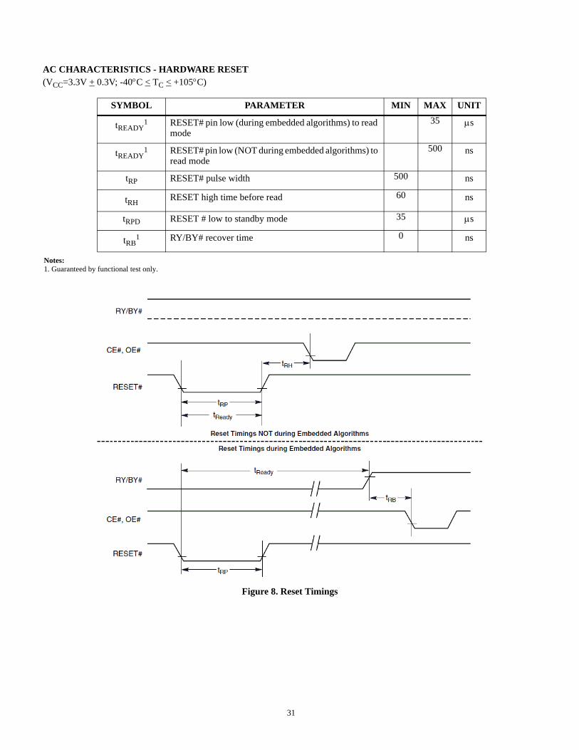
Table 12 shows the outputs for Data# Polling on DQ7. Figure 5 shows the Data# Polling algorithm. Figure 14 shows the Data# Polling timing diagram.

23
RY/BY#: Ready/Busy#The RY/BY# is a dedicated, open-drain output pin which indi-cates whether an Embedded Algorithm is in progress or com-plete. The RY/BY# status is valid after the rising edge of thefinal WE# pulse in the command sequence. Since RY/BY# is anopen-drain output, several RY/BY# pins can be tied together inparallel with a pull-up resistor to VCC.
If the output is low (Busy), the device is actively erasing or pro-gramming. This includes programming in the Erase Suspendmode. If the output is high (Ready), the device is in the readmode, the standby mode, or one of the banks is in the erase-sus-pend-read mode. Table 12 shows the outputs for RY/BY#.
When DQ5 is set to a logic 1, RY/BY# will be in the BUSYstate, or a logic 0.
Figure 5. Data# Polling Algorithm

24
DQ6: Toggle Bit IToggle Bit I on DQ6 indicates whether an Embedded Programor Erase algorithm is in progress or complete, or whether thedevice has entered the Erase Suspend mode. Toggle Bit I maybe read at any address, and is valid after the rising edge of thefinal WE# pulse in the command sequence (prior to the pro-gram or erase operation) and during the sector erase time-out.
During an Embedded Program or Erase algorithm operation,successive read cycles to any address cause DQ6 to toggle.The system may use either OE# or CE# to control the readcycles. When the operation is complete, DQ6 stops toggling.
After an erase command sequence is written, if all sectorsselected for erasing are protected, DQ6 toggles for approxi-mately 3 ms, then returns to reading array data. If not allselected sectors are protected, the Embedded Erase algorithmerases the unprotected sectors, and ignores the selected sectors
that are protected.
The system can use DQ6 and DQ2 together to determinewhether a sector is actively erasing or is erase suspended.When the device is actively erasing (that is, the EmbeddedErase algorithm is in progress), DQ6 toggles. When the deviceenters the Erase Suspend mode, DQ6 stops toggling. However,the system must also use DQ2 to determine which sectors areerasing or erase-suspended. Alternatively, the system can useDQ7.
If a program address falls within a protected sector, DQ6 tog-gles for approximately 1s after the program commandsequence is written, then returns to reading array data. DQ6also toggles during the erase-suspend-program mode, andstops toggling once the Embedded Program algorithm is com-plete.

25
Figure 6. Toggle Bit Algorithm

26
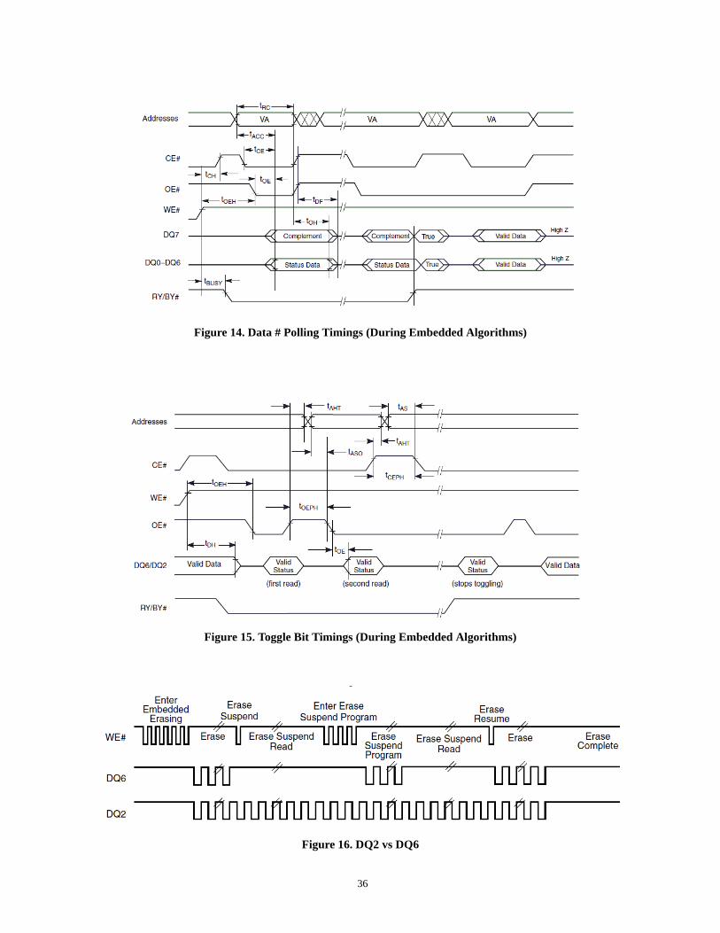
DQ2: Toggle Bit IIThe Toggle Bit II on DQ2, when used with DQ6, indicates whether a particular sector is actively erasing. That is, the Embedded Erase algorithm is in progress, or whether that sector is erase-suspended. Toggle Bit II is valid after the rising edge of the final WE# pulse in the command sequence.
DQ2 toggles when the system reads at addresses within those sectors that have been selected for erasure. The system may use either OE# or CE# to control the read cycles. DQ2 cannot distinguish whether the sector is actively erasing or is erase-suspended. DQ6, by comparison, indicates whether the device is actively erasing, or is in Erase Sus-pend, but cannot distinguish which sectors are selected for erasure. Thus, both status bits are required for sector and mode information.
Figure 6 shows the toggle bit algorithm in flowchart form. Figure 15 shows the toggle bit timing diagram. Figure 16 shows the differences between DQ2 and DQ6 in graphical form.
Reading Toggle Bits DQ6/DQ2Whenever the system initially begins reading toggle bit status, it mustread [DQ15:0] (or[ DQ7:0] for x8-only mode) at least twice in a rowto determine whether a toggle bit is toggling. Typically, the systemwould note and store the value of the toggle bit after the first read.After the second read, the system would compare the new value of thetoggle bit with the first. If the toggle bit is not toggling, the device hascompleted the program or erase operation. The system can read arraydata on [DQ15:0] (or [DQ7:0] for x8-only mode) on the followingread cycle.
However, if after the initial two read cycles, the system determinesthat the toggle bit is still toggling, the system also should notewhether the value of DQ5 is high. If it is, the system should thendetermine again whether the toggle bit is toggling, since the toggle bitmay have stopped toggling just as DQ5 went high. If the toggle bit isno longer toggling, the device has successfully completed the pro-gram or erase operation. If it is still toggling, the device did not com-pleted the operation successfully, and the system must write the resetcommand to return to reading array data.
The remaining scenario is that the system initially determines that the toggle bit is toggling and DQ5 has not gone high. The system may continue to monitor the toggle bit and DQ5 through successive read cycles, determining the status as described in the previous paragraph.
Alternatively, it may choose to perform other system tasks. In this case, the system must start at the beginning of the algorithm when it returns to determine the status of the operation. Please refer to Figure 6.
DQ5: Exceeded Timing LimitsDQ5 indicates whether the program or erase time has exceeded aspecified internal pulse count limit. Under these conditions DQ5 pro-duces a 1, indicating that the program or erase cycle was not success-fully completed.
The device may output a 1 on DQ5 if the system tries to program a 1 to a location that was previously programmed to 0. Only an erase operation can change a 0 back to a 1. Under this condition, the device halts the operation, and when the timing limit has been exceeded, DQ5 produces a 1. Under both these conditions, the system must write the reset command to return to the read mode or to the erase-suspend-read mode if a bank was previously in the erase-suspend-pro-gram mode.
DQ3: Sector Erase TimerAfter writing a sector erase command sequence, the system may read DQ3 to determine whether or not erasure has begun. The sector erase timer does not apply to the chip erase command. If additional sectors are selected for erasure, the entire time-out also applies after each additional sector erase command. When the time-out period is com-plete, DQ3 switches from a 0 to a 1. If the time between additional sector erase commands from the system can be assured to be less than 50s, the system need not to monitor DQ3. Refer to Sector Erase Command Sequence section.
After the sector erase command is written, the system should read the status of DQ7 (Data# Polling) or DQ6 (Toggle Bit I) to ensure that the device has accepted the command sequence, and then read DQ3. If DQ3 is 1, the Embedded Erase algorithm has begun; all further com-mands (except Erase Suspend) are ignored until the erase operation is complete. If DQ3 is 0, the device will accept additional sector erase commands. To ensure the command has been accepted, the system software should check the status of DQ3 prior to and following each subsequent sector erase command. If DQ3 is high on the second status check, the last command might not have been accepted. The RY/BY# pin will be in the BUSY state under this condition.
Table 12 shows the status of DQ3 relative to the other status bits.

27
Special Handling and Device InformationThe UT8QNF8M8 64Mbit flash memory device does not receive radiographic inspection from Aeroflex. Aeroflex will not warrantdevices that receive radiographic inspections. Devices are delivered in the all F’s (erased) state.
Notes:1. Data retention table is predicted on initial user programmed cycle of the device.
Table 12: Write Operation Status
STATUS DQ7 DQ6 DQ5 DQ3 DQ2 RY/BY#
Standard Mode
Embedded Program Algorithm DQ7# Toggle 0 N/A No toggle 0
Embedded Erase Algorithm
In busy erasing sector
0 Toggle 0 1 Toggle 0
In not busy erasing sector
0 Toggle 0 1 No toggle 0
Erase Suspend
Mode
Erase-Suspend-Read
Erase Suspended Sector
1 No toggle 0 N/A Toggle 1
Non-Erase Suspended Sector
Data Data Data Data Data 1
Erase-Suspend-Program DQ7# Toggle 0 N/A N/A 0
Table 13: Endurance and Retention
PARAMATER CONDITION LIMIT UNITS
Minimum data retention1 TC=105oC 5 Years
TC=90oC 21
TC=75oC 85
TC=60oC 350
Minimum endurance TC=-40oC to 105oC 10k Cycles per sector

28
OPERATIONAL ENVIRONMENT
Notes:1. The UT8QNF8M8 will not latch up during radiation exposure under recommended operating conditions.2. 90% worst case particle environments, geosynchronous orbit, 100 Mils of aluminum.3. Irradiated per MIL-STD-883 Method 1019 Condition C at 50-300 krad(Si) using an in-situ 900 rad(Si) device unpowered and 100 rad(Si) device statistically biased
duty cycle repeated 50 times to achieve a TID level of 50 krad(Si). This irradiation in-situ biasing method is predicated on an application which may allow the device to be unpowered during 90% of the mission life.
ABSOLUTE MAXIMUM RATINGS1
(Referenced to VSS)
Notes:1. Stresses above those listed under “Absolute Maximum Ratings” may cause permanent damage to the device. This is a stress rating only; functional operation of
the device at these or any other conditions above those indicated in the operational sections of this data sheet is not implied. Exposure of the device to absolute maximum rating conditions for extended periods may affect device reliability.
2. No more than one output may be shorted to ground at a time. Duration of the short circuit should not be greater than one second.3. Meets ESD testing per MIL-STD-883, Method 3015, Class 2.
RECOMMENDED OPERATING CONDITIONS
PARAMETER LIMIT UNITS
Total Ionizing Dose (TID)3 10 or 50 krad(Si)
Single Event Latchup (SEL)1 <80 MeV-cm2/mg @ 105oC
Single Event Upset (SEU)2 <102 MeV-cm2/mg @ 25oC
SYMBOL PARAMETER LIMITS
TSTG Storage temperature -65oC to +150oC
VCC DC Supply voltage -0.3V to +4.0V
VIO Voltage on any pin -0.3V to VCC +0.3V
IOS2 Output short circuit current 200 mA
II DC input current +10 mA
JC Thermal resistance, junction to case 8 oC/W
PD Power dissipation permitted at Tc=105oC 1 W
TJ Maximum junction temperature +150oC
ESDHBM3 ESD Rating 2000V
SYMBOL PARAMETER LIMITS
TC Operating case temperature -40 to +105oC
VCC Operating supply voltage 3.0V to 3.6V
VIN DC input voltage VSS to VCC

29
DC ELECTRICAL CHARACTERISTICS (VCC=3.3V + 0.3V; -40C < TC < +105C)
Notes:1. Maximum ICC specifications are tested with VCC = VCCmax.
2. ICC active while embedded erase or embedded program is in progress.
3. Automatic sleep mode enables the low power mode when addresses remain stable for tACC + 30ns. Typical sleep mode current is 200 nA.
4. Post radiation limits are the 105oC temperature limits when specified.5. Guaranteed by functional test only.
SYMBOL PARAMETER CONDITION MIN MAX UNIT
IIN Input leakage current VIN = VSS to VCC,
VCC = VCC max
+1.0 A
IOZ Output leakage current VOUT = VSS to VCC,
VCC = VCC max, OE# = VIH
+1.0 A
ICC11
VCC active read current
CE# = VIL, OE# = VIH,
Byte Mode
5MHz 16 mA
1 MHz 4 mA
CE# = VIL, OE# = VIH,
Word Mode
5 MHz 16 mA
1 MHz 4 mA
ICC21,2 VCC active write current/erase current CE# = VIL, OE# = VIH, WE# = VIL 30 mA
ICC31,4 VCC standby current CE#, RESET# = VCC + 0.3V Room &
-40oC
5 A
105oC 20 A
ICC41,4 VCC reset current RESET# = VSS + 0.3V Room &
-40oC
5 A
105oC 20 A
ICC51,3,4 Automatic sleep mode VIH = VCC + 0.3V;
VIL = VSS + 0.3V;
Room &
-40oC
5 A
105oC 20 A
VIH Input high voltage 2.1 V
VIL Input low voltage 0.8 V
VOL Output low voltage IOL = 2.0 mA, VCC = VCC min 0.45 V
VOH1 Output high voltage IOH = 2.0 mA, VCC = VCC min 2.4 V
VOH2 Output high voltage IOH = 100 A, VCC = VCC min VCC-0.4
V
VLKO5 Low VCC lock-out voltage 1.8 V

30
AC CHARACTERISTICS - READ ONLY OPERATIONS (VCC=3.3V + 0.3V; -40C < TC < +105C)
Notes:1. Guaranteed by functional test only.2. Measurements performed by placing a 50 ohm termination on the data pin with a bias of VCC/2 or equivalent. The time from control high to the data bus transition-
ing to VCC/2 +100 mV is taken as tDFXX.
SYMBOL PARAMETER MIN MAX UNIT
tRC1 Read cycle tine 60 ns
tACC Address to output delay 60 ns
tCE Chip enable to output delay 60 ns
tOE Output enable to output delay 25 ns
tDFCE1, 2 Chip enable to output High-Z 20 ns
tDFOE1, 2 Output enable to output High-Z 16 ns
tOH Output hold time from addresses, CE# or OE#, whichever occurs first
0 ns
tOEH1 Output enable hold time - read
Output enable hold time - toggle and data# polling0 ns
5 ns
Figure 7. Read Operations Timing
31
AC CHARACTERISTICS - HARDWARE RESET (VCC=3.3V + 0.3V; -40C < TC < +105C)
SYMBOL PARAMETER MIN MAX UNIT
tREADY1 RESET# pin low (during embedded algorithms) to read
mode35 s
tREADY1 RESET# pin low (NOT during embedded algorithms) to
read mode500 ns
tRP RESET# pulse width 500 ns
tRH RESET high time before read 60 ns
tRPD RESET # low to standby mode 35 s
tRB1 RY/BY# recover time 0 ns
Figure 8. Reset Timings
Notes:1. Guaranteed by functional test only.

32
AC CHARACTERISTICS - WORD/BYTE CONFIGURATION (BYTE #)(VCC=3.3V + 0.3V; -40C < TC < +105C)
SYMBOL PARAMETER MIN MAX UNIT
tELFL/tELFH1 CE# to BYTE# switching low or high 5 ns
tFLQZ2 BYTE# switching low to output High-Z 16 ns
tFHQV BYTE# switching high to output active 60 ns
Figure 9. Byte# Timings for Read Operations
Figure 10. Byte# Timings for Write Operations
Notes:1. Guaranteed by functional test only.2. Measurements performed by placing a 50 ohm termination on the data pin with a bias of VCC/2 or equivalent. The time from control high to the data bus transition-
ing to VCC/2 +100 mVis taken as tELXX.

33
ERASE AND PROGRAM OPERATIONS (VCC=3.3V + 0.3V; -40C < TC < +105C)
Notes:1. Guaranteed by functional test only.2. See Erase and Programming Performance on page 39 for more information.3. Supplied as a design limit, neither tested nor guaranteed.
SYMBOL PARAMETER MIN MAX UNIT
tWC1 Write cycle tine 60 ns
tAS1 Address setup time 0 ns
tASO1 Address setup time to OE# low during toggle bit polling 15 ns
tAH1 Address hold time 35 ns
tAHT1 Address hold time from CE# or OE# high during toggle bit polling 0 ns
tDS1 Data setup time 35 ns
tDH1 Data hold time 0 ns
tOEPH1 Output enable high during toggle bit polling 20 ns
tCS1 CE# setup time 0 ns
tCH1 CE# hold time 0 ns
tWP1 Write pulse width 25 ns
tWPH1 Write pulse width high 25 ns
tSR/W1 Latency between read and write operations 0 ns
tWHWH11 Programming operation Byte 6 s
Word 6 s
tWHWH21,2 Sector erase operation 0.5 sec
tVCS3 VCC setup time 50 s
tRB1 Write recovery time from RY/BY# 0 ns
tBUSYProgram/Erase valid to RY/BY# delay 90 ns
tESL3 Erase suspend latency 35 s

34
Figure 11. Program Operation Timings

35
Figure 13. Back-to-Back Read/Write Timings
Figure 12. Chip/Sector Erase Operation Timings
36
Figure 14. Data # Polling Timings (During Embedded Algorithms)
Figure 15. Toggle Bit Timings (During Embedded Algorithms)
Figure 16. DQ2 vs DQ6

37
ALTERNATE CE# CONTROLLED ERASE AND PROGRAM OPERATIONS(VCC=3.3V + 0.3V; -40C < TC < +105C)
Notes:1. Guaranteed by functional test only.2. See Erase and Programming Performance on page 39 for more information.
SYMBOL PARAMETER MIN MAX UNIT
tWC1 Write cycle 60 ns
tAS1 Address setup time 0 ns
tAH1 Address hold time 35 ns
tDS1 Data setup time 35 ns
tDH1 Data hold time 0 ns
tGHEL1 Read recovery time below write
(OE# high to WE# low)0 ns
tWS1 WE# setup time 0 ns
tWH1 WE# hold time 0 ns
tCP1 CE# pulse width 25 ns
tCPH1 CE# pulse width high 25 ns
tWHWH11,2 Programming operation Byte 6 s
Word 6 s
tWHWH21,2 Sector erase operation 0.5 sec

38
Figure 17. Alternate CE# Controlled Write (Erase/Program)

39
ERASE AND PROGRAMMING PERFORMANCE (VCC=3.3V + 0.3V; -40C < TC < +105C)
PIN CAPACITANCE
AC TEST LOAD CIRCUIT
PARAMETER MAX UNIT
Sector erase time 5 sec
Chip erase time 120 sec
Byte program time1 150 s
Word program time1 150 s
PARAMETER DESCRIPTION TEST SETUP MAX UNIT
CIN Input capacitance (applies to A21-A0, DQ15-DQ0) VIN = 0 15 pF
COUT Output capacitance (applies to DQ15-DQ0, RY/BY#) VOUT= 0 15 pF
CIN2 Control pin capacitance (applies to CE#, WE#, RESET#, BYTE#)
VIN = 0 15 pF
CIN3 Control pin capacitance (applies to WP#)) VIN = 0 25 pF
Note:1. Guaranteed by functional test only.

40
Package Drawing
Figure 18. 48-pin Ceramic Flatpack Package

41
Ordering Information
UT8QNF8M8
UT ****** - * * * * *
Lead Finish: (Note 1)(C) = Gold
Screening: (Note 2,3)(E) = HiRel (Temperature Range: -40C to +105C)
(P) = Prototype flow (Temperature Range: 25oC only)(T) = Prototype flow (Temperature Range:-40C to +105C )
Package Type:(X) = 48-lead Ceramic Flat Package
Access Time:(60) = 60ns access time
Device Type:(8QNF8M8) = 64Mb NOR Flash
Notes:1. Lead finish is "C" (Gold) only.2. Prototype flow per Aeroflex Colorado Springs Manufacturing Flows Document. Radiation neither tested nor guaranteed.3. HiRel flow per Aeroflex Colorado Springs Manufacturing Flows Document. Radiation neither tested nor guaranteed.
42
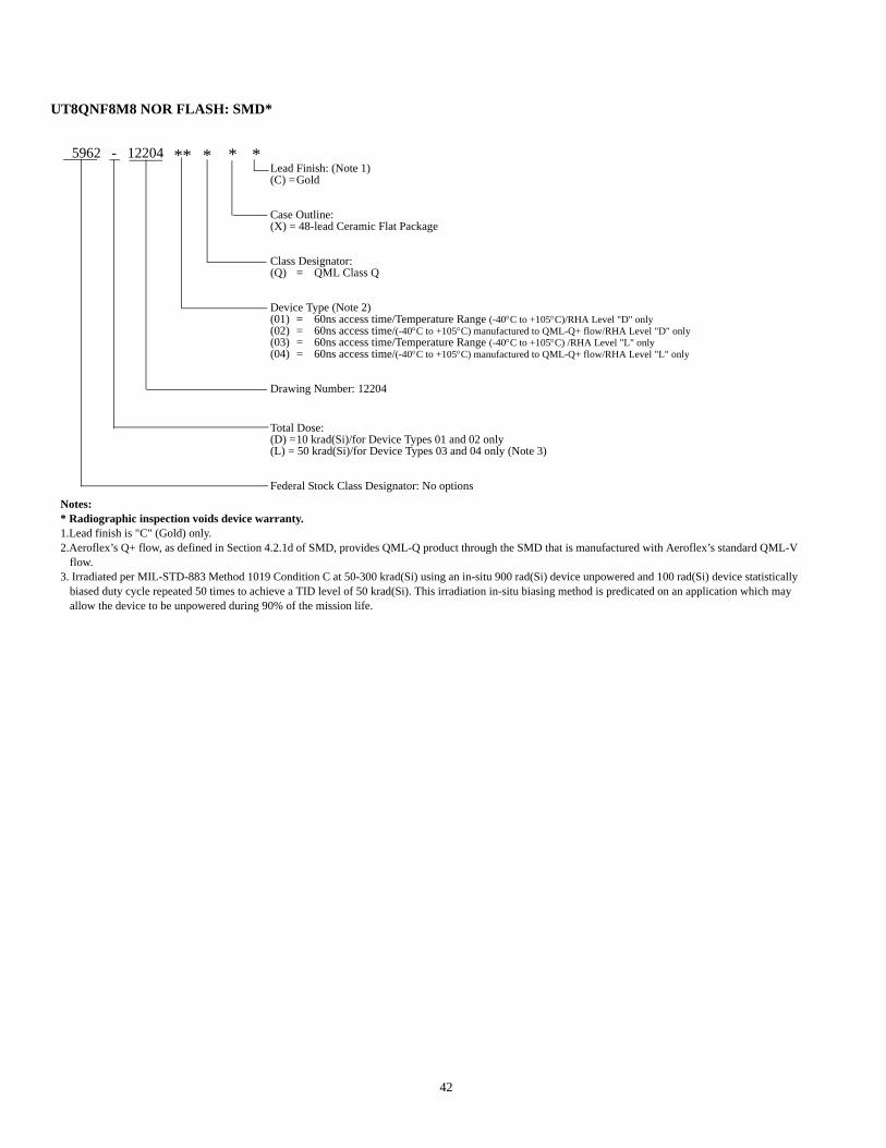
UT8QNF8M8 NOR FLASH: SMD*
5962 - 12204 Lead Finish: (Note 1)(C) =Gold
Case Outline:(X) = 48-lead Ceramic Flat Package
Class Designator:(Q) = QML Class Q
Device Type (Note 2)(01) = 60ns access time/Temperature Range (-40C to +105C)/RHA Level "D" only(02) = 60ns access time/(-40C to +105C) manufactured to QML-Q+ flow/RHA Level "D" only(03) = 60ns access time/Temperature Range (-40C to +105C) /RHA Level "L" only(04) = 60ns access time/(-40C to +105C) manufactured to QML-Q+ flow/RHA Level "L" only(02TBD)=15ns access time, CMOS I/O, 40-lead flatpack package, dual chip enable (not available)
Drawing Number: 12204
Total Dose:(D) =10 krad(Si)/for Device Types 01 and 02 only(L) = 50 krad(Si)/for Device Types 03 and 04 only (Note 3)
Federal Stock Class Designator: No options
Notes:* Radiographic inspection voids device warranty.1.Lead finish is "C" (Gold) only.2.Aeroflex’s Q+ flow, as defined in Section 4.2.1d of SMD, provides QML-Q product through the SMD that is manufactured with Aeroflex’s standard QML-V
flow.3. Irradiated per MIL-STD-883 Method 1019 Condition C at 50-300 krad(Si) using an in-situ 900 rad(Si) device unpowered and 100 rad(Si) device statistically
biased duty cycle repeated 50 times to achieve a TID level of 50 krad(Si). This irradiation in-situ biasing method is predicated on an application which may allow the device to be unpowered during 90% of the mission life.
** * **

43
COLORADO Toll Free: 800-645-8862 Fax: 719-594-8468
SE AND MID-ATLANTIC Tel: 321-951-4164 Fax: 321-951-4254
INTERNATIONALTel: 805-778-9229Fax: 805-778-1980
WEST COAST Tel: 949-362-2260Fax: 949-362-2266
NORTHEASTTel: 603-888-3975Fax: 603-888-4585
CENTRALTel: 719-594-8017Fax: 719-594-8468
w w w . a e r o f l e x . c o m i n f o - a m s @ a e r o f l e x . c o m
Our passion for performance is defined by threeattributes represented by these three icons:
solution-minded, performance-driven and customer-focused
Aeroflex Colorado Springs (Aeroflex) reserves the right to make changes to any products and services herein at any time without notice. Consult Aeroflex or an authorized sales representative to verify that the information in this data sheet is current before using this product. Aeroflex does not assume any responsibility or liability arising out of the application or use of any product or service described herein, except as expressly agreed to in writing by Aeroflex; nor does the purchase, lease, or use of a product or service from Aeroflex convey a license under any patent rights, copyrights, trademark rights, or any other of the intellectual rights of Aeroflex or of third parties.
A e r o f l e x C o l o r a d o S p r i n g s - D a t a s h e e t D e f i n i t i o n
A d v a n c e d D a t a s h e e t - P r o d u c t I n D e v e l o p m e n t
P r e l i m i n a r y D a t a s h e e t - S h i p p i n g P r o t o t y p e
D a t a s h e e t - S h i p p i n g Q M L & H i - R e l
Related Documents