ICE Emulator for PowerPC 1 ©1989-2018 Lauterbach GmbH ICE Emulator for PowerPC TRACE32 Online Help TRACE32 Directory TRACE32 Index TRACE32 Documents ...................................................................................................................... ICE In-Circuit Emulator ................................................................................................................. ICE Target Guides ...................................................................................................................... ICE Emulator for PowerPC ..................................................................................................... 1 WARNING .............................................................................................................................. 5 Quick Start ............................................................................................................................ 6 Troubleshooting ................................................................................................................... 7 Hang-Up 7 Dualport Errors 7 FAQ ........................................................................................................................................ 8 Basics .................................................................................................................................... 9 SYStem.Mode 10 SYStem.Clock Clock generation 11 Dualport Modes 11 Mapping and CS Setting of the MPC505, PPC403 12 Mapping and CS setting of the MPC860/821 12 Jumper Settings of the MPC860/821 Probe 14 Adaption to different Clock Sources of the MPC860/821 Probe 15 Layout of the MPC860/821 Probe 16 General SYStem Settings and Restrictions ....................................................................... 19 General Restrictions 19 SYStem.Option PreMap Address lines 20 SYStem.Option PreMapMod Premapper mode 20 SYStem.Option TestClock Clock test 21 SYStem.Option BreakMask Break mask 22 SYStem.Option FREEZE Timer freeze modes 22 SYStem.Option VSYNC Synch trace signals 23 SYStem.Option CFLUSH Instruction cache flush 23 SYStem.Option ONCE On-circuit emulation 23 SYStem.Option BASE Peripheral base address 24 SYStem.Option RESETCONF Reset configuration 24 SYStem.Option IBUS IBUS control 24 SYStem.Option ICFLUSH Internal instruction cache flush 24

Welcome message from author
This document is posted to help you gain knowledge. Please leave a comment to let me know what you think about it! Share it to your friends and learn new things together.
Transcript

ICE Emulator for PowerPC
TRACE32 Online Help
TRACE32 Directory
TRACE32 Index
TRACE32 Documents ......................................................................................................................
ICE In-Circuit Emulator .................................................................................................................
ICE Target Guides ......................................................................................................................
ICE Emulator for PowerPC ..................................................................................................... 1
WARNING .............................................................................................................................. 5
Quick Start ............................................................................................................................ 6
Troubleshooting ................................................................................................................... 7
Hang-Up 7
Dualport Errors 7
FAQ ........................................................................................................................................ 8
Basics .................................................................................................................................... 9
SYStem.Mode 10
SYStem.Clock Clock generation 11
Dualport Modes 11
Mapping and CS Setting of the MPC505, PPC403 12
Mapping and CS setting of the MPC860/821 12
Jumper Settings of the MPC860/821 Probe 14
Adaption to different Clock Sources of the MPC860/821 Probe 15
Layout of the MPC860/821 Probe 16
General SYStem Settings and Restrictions ....................................................................... 19
General Restrictions 19
SYStem.Option PreMap Address lines 20
SYStem.Option PreMapMod Premapper mode 20
SYStem.Option TestClock Clock test 21
SYStem.Option BreakMask Break mask 22
SYStem.Option FREEZE Timer freeze modes 22
SYStem.Option VSYNC Synch trace signals 23
SYStem.Option CFLUSH Instruction cache flush 23
SYStem.Option ONCE On-circuit emulation 23
SYStem.Option BASE Peripheral base address 24
SYStem.Option RESETCONF Reset configuration 24
SYStem.Option IBUS IBUS control 24
SYStem.Option ICFLUSH Internal instruction cache flush 24
ICE Emulator for PowerPC 1 ©1989-2018 Lauterbach GmbH

SYStem.Option ICREAD Instruction cache read 25
SYStem.Option DCREAD Date cache read 25
SYStem.Option WATCHDOG Disable watchdog 25
SYStem.Option BRKNOMSK tbd. 25
SYStem.Option FlowTrace tbd. 26
SYStem.Option ResetExt tbd. 26
SYStem.Option ResetMode tbd. 26
SYStem.Option SCRATCH tbd. 27
SYStem.Option TURBO tbd. 27
SYStem.Option Wait System wait states 27
Exception Control ................................................................................................................ 28
Schematics 28
RESET 29
eXception.Activate Force exception 30
eXception.Enable Enable exception 32
eXception.Pulse Stimulate exception 33
Mapping ................................................................................................................................. 35
MAP.BUS Bus width mapping 35
CPU specific MMU commands ............................................................................................ 36
MMU.TLB Display MMU TLB entries 36
MMU.TLBSCAN Load MMU TLB entries 36
Memory Classes ................................................................................................................... 37
State Analyzer ....................................................................................................................... 38
Keywords for the Trigger Unit 38
Keywords for the Display 38
Port Analyzer ........................................................................................................................ 39
Keywords for the Port Analyzer 39
Additional Trace Channels 41
Module PPC403GA 41
Module MPC505 41
Module MPC860/MPC821 42
Compilers .............................................................................................................................. 43
3rd Party Tool Integrations .................................................................................................. 44
Realtime operation Systems ............................................................................................... 46
Emulation Modules .............................................................................................................. 48
Module Overview 48
Order Information 49
Operating Voltage ................................................................................................................ 50
Physical Dimensions ........................................................................................................... 51
ICE Emulator for PowerPC 2 ©1989-2018 Lauterbach GmbH

Adapter .................................................................................................................................. 58
ICE Emulator for PowerPC 3 ©1989-2018 Lauterbach GmbH

ICE Emulator for PowerPC
Version 16-Nov-2018
For general informations about the In-Circuit Debugger refer to the “ICE User’s Guide” (ice_user.pdf). All general commands are described in “PowerView Command Reference” (ide_ref.pdf) and “General Commands and Functions”.
/
P:FFF00FC4 \\DIABC1\main ..DA....T.... MIX
E::w.d.l E::w.peraddr/line code label mne
535 { Processor VersionP:FFF00FC4 9421FFD8 main: stw PVR 00200001 FAM 00000002 MEP:FFF00FC8 7C0802A6 mfl MAJ 00000000 MIP:FFF00FCC 93E10024 stwP:FFF00FD0 9001002C stw Timer
int j; TSR 44000000 WIS pending WRchar * p; TCR 00000000 WP 2^17 WPC of
PIE disable FP539 vtripplearray[0][0][0 PIT 00000000
E::w.a.lrecord run address cycle d.l symbol
-000003 f P:FFF00FC4 fetch 7FE00008 \\DIABC1\main 1532533 E::w.v.l534 main() main()535 { j = 1
trap p = 0x0-000002
mflr r0-000001 BRK
ICE Emulator for PowerPC 4 ©1989-2018 Lauterbach GmbH

WARNING
NOTE: Do not connect or remove probe from target while target power is ON.
Power up: Switch on emulator first, then targetPower down: Switch off target first, then emulator
ICE Emulator for PowerPC 5 ©1989-2018 Lauterbach GmbH

Quick Start
tbd.
ICE Emulator for PowerPC 6 ©1989-2018 Lauterbach GmbH

Troubleshooting
Hang-Up
tbd.
Dualport Errors
tbd.
ICE Emulator for PowerPC 7 ©1989-2018 Lauterbach GmbH

FAQ
ICE Emulator for PowerPC 8 ©1989-2018 Lauterbach GmbH

Basics
The ICE-PPC emulation head supports MPC500 and MPC800 series derivatives from Freescale Semiconductor and PPC400 series derivatives from IBM:
• PPC403GA
• MPC505
• MPC821
• MPC860
The adaption to different probes is done by changing the module. Modules support BGA or QFP versions, where applicable. The emulation frequency is up to 20MHz with 0 wait states and up to 28 MHz with 1 or more wait states. There is no significant speed difference to realtime because target systems in most cases use wait states and fast program loops are running from the cache. This leads to an average performance reduction of only about 10% using three wait states.
The probe uses a special emulation concept (active/passive emulation) to provide either emulation in realtime in the target or the advanced emulation features of Trace32 with reduced speed.
Therefore the probe contains three parts. The top level is the passive emulation module. It contains the drivers for addresses, data and ports, the control for the bus interface, the dualport and the BDM. The second level is the active CPU module, it contains the CPU, the interrupt-, reset-enable and the clock switches, the pull-up resistors for the CPU and the control of the switches and the buffers on the buffer module. The third level is the buffer module. It contains the address and data buffers between the CPU and the target. The modules are connected with the target connector for the CPU signals (e.g ET160) and additional an intermodul connector for the control signals. You can put these three modules one on the other.
If you want to use all emulation features (Internal mode, internal mapping, internal clock) you need all three of the modules.
If you want more speed in your target memory, you can leave out the buffer module (the buffers have a few ns delay). The restriction now is, that you can map internal memory only if no buffer on your target is decoded at the same address, and that the synchronous breakpoints does not work with external memory. If your target memory is a ram, you can use software breakpoints instead.
If you have already soldered a CPU on your target, you can work in passive emulation. You need only the passive module. The CPU on your target is operated via the BDM port. Advantage is, that there is no time delay. Restrictions: Same as above and also no internal clock mode and no enable/disable of the interrupts and the reset lines.
An additional slot in the base modul offers upgrading with the port analyzer to get timing and state of the CPU ports.
We use a different system for numbering the address and data lines as it is used in the PowerPC descriptions. Our least significant bit is called D0 or A0, the MSB D31 or A31. Don't be confused, if you find some differences between your databook and perhaps our peripheral window.
ICE Emulator for PowerPC 9 ©1989-2018 Lauterbach GmbH

SYStem.Mode
The emulation head can stay in 6 modes. The modes are selected by the SYStem.Up or the SYStem.Mode command.
In active mode, the power of the target is sensed and by switching down the target the emulator changes to RESET mode. The probe is not supplied by the target. When running without target, the target voltage is simulated by an internal pull-up resistor.
Format: SYStem.Mode <mode>
<mode>: ResetDownResetUpAloneIntAloneExtEmulIntEmulExt
Reset Down Target is down, all drivers are in tristate mode.
Reset Up Target has power, drivers are logically in inactive state, but not tristate.
Alone Internal Probe is running with internal clock, driver inactive. (Only with active module and buffer module.)
Alone External Probe is running with external clock, driver inactive. (Only with active module and buffer module.)
Emulation Internal Probe is running with internal clock, strobes to target are generated. (Only with active module, buffer module optional)
Emulation External Probe is running with external clock, strobes to target are activated. (Active module and buffer module optional)
E::w.syssystem Mode Clock TimeReq OptionDown RESet VCO 1.000ms PreMap
Up Analyzer Low TimeOut TestClockMonitor Mid 50.000us Option
RESet ResetDown High 0.ResetUp Wait
cpu-type NoProbe Access 0.PPC403 AloneInt Nodelay25 MHz AloneExt Wait
EmulInt RequestEmulExt Denied
ICE Emulator for PowerPC 10 ©1989-2018 Lauterbach GmbH

SYStem.Clock Clock generation
Dualport Modes
Dualport access modes.
Format: SYStem.Clock <option>
<option>: VCOHighMidLow
VCO Variable frequency 1 … 35 MHz.
Low, Mid, High
2.5, 5.0 or 10.0 MHz.
Format: SYStem.Access <mode>
<mode>: RequestDenied
Request The CPU bus access is stopped by the bus request signals for dualport access.
Denied No dualport access is allowed while the realtime emulation is running.
ICE Emulator for PowerPC 11 ©1989-2018 Lauterbach GmbH

Mapping and CS Setting of the MPC505, PPC403
The PowerPC controllers have bus interfaces, which allows the CPU to communicate with the external memory and peripherals without external logic. In the emulator, we use an epld to rebuild an address and data strobe out of the different chipselect lines of the CPU. For programming this epld, it is necessary for us to know, how the user has programmed the bus interface.
So, it is necessary for us to know these settings before delivering, to adapt this reconstruction epld to your target.
If the CS settings change during the project, it is possible to reprogram this epld. It is possible to reprogram it by sending a programming batch file to the customer.
Mapping and CS setting of the MPC860/821
Normally, it is possible to map the user ram of an MPC860 emulator without any application specific epld. The following rules should enable you to make your own mapping:
1. Set the SYS.OPTION PreMapModule off
2. Set your CS registers in the way you want the mapping. If you use the UPMA or UPMB DRAM access, the start address multiplex bit (CSNT/SAM) in the option register of the CS must be 0. The emulator uses the first cycle of the memory access to latch the internal addresses. With this bit at 0, the first cycle of the DRAM access is not multiplexed, but shows the internal addresses on the address pins. For accessing your target memory, it is necessary to change the programming of the UPM RAM. It is recommended to use internal emulation memory instead of the external target DRAM. Then, you don’t have to care for the UPM settings. Find more Information about this matter in the chapters External Bus Interface and Memory Controller of the user manual
CLKOUT
TS
TA
ADDR
DATA
ROW COLLUMN
RAS/CS
CAS
Typical DRAM Access0 WaitstatesSAM = 1
ICE Emulator for PowerPC 12 ©1989-2018 Lauterbach GmbH

3. Map workbenches wherever you need ram.
4. Map RAM wherever you need it. Map the bus size to the RAM location.
Example:
SYS.DOWN
MAP.RESET
SYS.O PMM OFF
SYS.M AI
d.s 0x2200110 %l 0x000800081Set BR CS2d.s 0x2200114 %l 0x0FC00800Set OR CS2MAP.PRE 0x0--0x0FFFFF
MAP.RAM 0x0--0x0FFFFMAP 64 KMAP.BUS32 0x0--0x0FFFF32 BitMAP.Iinternal
CLKOUT
TS
TA
ADDR
DATA
ROW COLLUMN
RAS/CS
CAS
INT
Typical DRAM Access
0 WaitstatesSAM = 0
ICE Emulator for PowerPC 13 ©1989-2018 Lauterbach GmbH

Jumper Settings of the MPC860/821 Probe
Some lines of the MPC860 CPU are connected with the target and can be disconnected by removing a jumper, if they cause problems to the target.
PORESET has a 4.7K pull-up and will be asserted with every system.up
RSTCONF has a 1K pull-down
MODCK has pull-up/pull-down as configured. Ref.: Adaption to different clock sources
Look in Layout of the MPC860/821 probe for the physical location of the jumpers.
Target
CPU
MODCK1
MODCK2
RSTCONF
PORESET
J660J657J658J659
ICE Emulator for PowerPC 14 ©1989-2018 Lauterbach GmbH

Adaption to different Clock Sources of the MPC860/821 Probe
MPC860 Clock source selection is made by sampling the MODCK1 and MODCK2 pins during Power On Reset (POR). The POR is asserted during every sys.up command. The emulation pod has 4.7K pull-up at MODCK1 and 4.7K pull-down at MODCK2 as default. This is the 1:1 mode setting of the CPU clock. For adapting to different clock sources, you may change the pull-up/down resistors as needed.
Look in Layout of the MPC860/821 probe for the physical location of the jumpers.
MODCK1 MODCK2 Default MF+1
SPLL Options
0 0 513 Normal Operation, PLL Enabled. Timing reference is freq (OSCM) = 32 kHz
0 1 5 Normal Operation, PLL Enabled. Timing reference is freq (OSCM) = 4 MHz
1 0 1 Normal Operation, PLL Enabled. 1:1 ModeF (clkout) = F (extclk)
1 1 5 Normal Operation, PLL Enabled. Timing reference is freq (OSCM) = 4 MHz
Target
CPU
VCCGND
MODCK1
MODCK2 J651
R650J650
R651
J658J659
ICE Emulator for PowerPC 15 ©1989-2018 Lauterbach GmbH
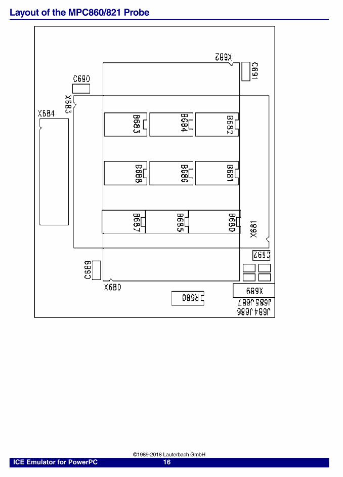
Layout of the MPC860/821 Probe
ICE Emulator for PowerPC 16 ©1989-2018 Lauterbach GmbH

ICE Emulator for PowerPC 17 ©1989-2018 Lauterbach GmbH

ICE Emulator for PowerPC 18 ©1989-2018 Lauterbach GmbH

General SYStem Settings and Restrictions
General Restrictions
Turbo Control (400 fam-ily)
Make sure, that you don't increase the debug clock without decreasing the internal wait states, when the TURBO option is enabled. If external wait states are used it is recommended to switch TURBO mode off.
Trace Information (400 family)
The emulator needs the trace information on the TS pins. You must switch the realtime debug mode in the input/output configuration register to bus.
Exception Routines (500/800 family)
The CPU handles the debug mode similar to an exception. Therefore stepping through an interrupt service routine is not possible, because the execution of the RFI instruction forces the CPU to exit from debug mode. Also modifications of SRR0 and SRR1 are ignored when exiting debug mode. If it is necessary to debug an exception routine, you are allowed to do the following things: If the CPU is not in a recoverable state (after jump into the exception routine) no breakpoints are allowed. When the software of the exception has saved the MSR and IP and set the RI bit of the MSR, the CPU is in recoverable state and one is allowed to break the routine. After this break, the old srr0 and srr1 registers, which contain the information about the state of the CPU before the exception are overwritten and lost. You can now step through the exception routine till the srr0 and srr1 registers are recalled from the stack. After this program line till the RFI instruction is reached, stepping (neither HLL nor ASM steps) or breaks are not allowed anymore, but it is possible to leave the exception routine with a go command.While being in a non recoverable state, you can’t execute a go command
Clock Output (500/800 family)
The emulator needs the clockout frequency of the CPU, you must not switch off the clockout pin for power saving purposes.
Dualport For the dualport access, it is necessary for the emulator to have the control of the bus between the cycles of the CPU. The emulator uses the normal bus arbitration signals to stop the CPU cycles. If you want to use dualport access, no device on your target may drive an active high signal on the bus, because then the emulator would produce an bus collision. Use pull-up resistors instead.
ICE Emulator for PowerPC 19 ©1989-2018 Lauterbach GmbH

SYStem.Option PreMap Address lines
The emulator can run in 24- and 32-Bit mode. If the upper address lines are not used by the target system, the pre-mapper should be switched off.
We call the most significant address A31, in difference to the PPC description.
SYStem.Option PreMapMod Premapper mode
The emulator has two premapper. The first is the regular premapper, which uses the address lines 20 to 31. The second is the module premapper, which has defined the 16 workbenches to the CS signals and the address A20 (=A11 of the PowerPC) of the CPU. It is not as flexible a the regular premapper, but it is faster. Here, you can define your memory region for each workbench.
The sys.o pmm switches between the pre-mapper ram on the base and the project specific premap epld on the module.
.
Format: SYStem.Option PreMap [ON | OFF]
Bus width SYStem.Option PreMap
A0--A24 OFF
A0--A32 ON
Format: SYStem.Option PreMapMod [ON | OFF]]
A23-A20
SwitchA31- Normal Work WorkA20 Pre Bench Pre Bench
Mapper 0-15 Switch Map 0-15
Pre WorkCPU Map Bench
CS Mod 0-15
CS WorkPre BenchMapper 0-15
ICE Emulator for PowerPC 20 ©1989-2018 Lauterbach GmbH

For example:
You want to use CS2 at the address 0ff00000. If you want to use the module premapper type:
Now your map.pre window shows following:
If you want to use the regular premapper type:
Now your map.pre window shows following:
SYStem.Option TestClock Clock test
If this option is on, the emulator tests if there is a clock output of the CPU.
A20=0 A20=1
CS0 WB0 WB1
CS1 WB2 WB3
CS2 WB4 WB5
CS3 WB6 WB7
CS4 WB8 WB9
CS5 WB10 WB11
CS6 WB12 WB13
CS7 WB14 WB15
sys.o pmm onmap.pre 0x0ff00000++0x0fffff 4.map …
logical Workbench Address physical Workbench
1 0FF00000--0FFFFFFF 4
sys.o pmm offmap.pre 0x0ff00000++0x0fffffmap …
logical Workbench Address physical Workbench
1 0FF00000--0FFFFFFF 0
Format: SYStem.Option TestClock [ON | OFF]
ICE Emulator for PowerPC 21 ©1989-2018 Lauterbach GmbH

SYStem.Option BreakMask Break mask
Only MPC860, MPC821, MPC505
The cpu handles debug events similar to exceptions. When a debug event (normally a break) OR a exception occurs, the cpu copies the msr into srr1 and the ip into srr0. This means, that after an exception occurred, the old values of ip and msr are as backup in the srr0 and srr1 registers. If now a break happens, these values will be overwritten by the new msr and ip values. So, it is possible to return to the exception routine, but not to the main program. The status after the start of the exception routine is called non recoverable state.
If you want to break in a non recoverable state, you must switch the option BreakMask to on.
SYStem.Option FREEZE Timer freeze modes
If this option is on, the internal timer/counter are frozen when being in debug mode.
Format: SYStem.Option BreakMask [ON | OFF]
Format: SYStem.Option FREEZE [ON | OFF]
ICE Emulator for PowerPC 22 ©1989-2018 Lauterbach GmbH

SYStem.Option VSYNC Synch trace signals
Only MPC860, MPC821, MPC505
The emulator has the possibility to trace the flowtrace signals of the cpu with each clock cycle. With this trace, it is possible to reconstruct the instruction flow of the cpu, even if the cpu runs in the internal cache. To reconstruct this flow, it is necessary that the cpu makes a show cycle after each indirect branch (See register setting of the ICTRL register in your cpu manual) and, that the cpu makes one show cycle after the half of the clock trace.
The option VSYNC generates a VSYNC command to the cpu every 32000 clock cycles to force the cpu to make a show cycle.
SYStem.Option CFLUSH Instruction cache flush
Only MPC860, MPC821, MPC505
If you use the internal instruction cache, it is necessary to flush the cache before every go or hll step. Option CFLUSH enables the cache flush software before each jump in.
Warning: Problems can occur when the LCD driver of the MPC821 is active!!!
SYStem.Option ONCE On-circuit emulation
Only MPC860, MPC821
If you use the target connection via samtec connectors, and leave the CPU on the target, you can switch the CPU on the target to HI-Z state. For this option, it is necessary that the BDM/JTAG pins of the target CPU are in BDM mode after reset (default), and that the TRST pin is pulled to high with a resistor (1K - 10K).
Format: SYStem.Option VSYNC [ON | OFF]
Format: SYStem.Option CFLUSH [ON | OFF]
Format: SYStem.Option ONCE [ON | OFF]
ICE Emulator for PowerPC 23 ©1989-2018 Lauterbach GmbH

SYStem.Option BASE Peripheral base address
Only MPC860, MPC821
The internal peripherals of the cpu can be mapped at different places. Sys.o base defines the base address of the peripheral window. This option must be set before the peripheral window is activated. If it is changed later, you must reprogram the peripheral window with the command per.rp.
SYStem.Option RESETCONF Reset configuration
Only MPC860, MPC821
After HRESET is released, the reset configuration word is sampled from the data bus. With this option, you can define your reset configuration. The DBGC value is always 0x3 and the DBPC value is always 0.
SYStem.Option IBUS IBUS control
Only MPC860, MPC821
With this option, you can set the instruction fetch show cycle and serialize control bits of the IBUS support control register.
SYStem.Option ICFLUSH Internal instruction cache flush
If you use the internal instruction cache, it is necessary to flush the cache before every go or hll step. Option CFLUSH enables the cache flush software before each jump in.
Warning: Problems can occur when the LCD driver of the MPC821 is active!!!
Format: SYStem.Option BASE [<Value>]
Format: SYStem.Option RESETCONF [<Value>]
Format: SYStem.Option IBUS [<Value>]
Format: SYStem.Option ICFLUSH [ON | OFF]
ICE Emulator for PowerPC 24 ©1989-2018 Lauterbach GmbH

SYStem.Option ICREAD Instruction cache read
If this option is switched on, data dump considers the valid cache lines of the instruction cache. This can be different to the external memory.
SYStem.Option DCREAD Date cache read
If this option is switched on, data dump considers the valid cache lines of the data cache. This can be different to the external memory.
SYStem.Option WATCHDOG Disable watchdog
If this option is switched off, the watchdog timer of the CPU is disabled after the sys.up.
SYStem.Option BRKNOMSK tbd.
tbd.
Format: SYStem.Option ICREAD [ON | OFF]
Format: SYStem.Option DCREAD [ON | OFF]
Format: SYStem.Option WATCHDOG [ON | OFF]
Format: SYStem.Option BRKNOMSK [ON | OFF]
ON tbd.
OFF tbd.
ICE Emulator for PowerPC 25 ©1989-2018 Lauterbach GmbH

SYStem.Option FlowTrace tbd.
tbd.
SYStem.Option ResetExt tbd.
tbd.
SYStem.Option ResetMode tbd.
tbd.
Format: SYStem.Option FlowTrace [ON | OFF]
ON tbd.
OFF tbd.
Format: SYStem.Option ResetExt [ON | OFF]
ON tbd.
OFF tbd.
Format: SYStem.Option ResetMode [ON | OFF]
ON tbd.
OFF tbd.
ICE Emulator for PowerPC 26 ©1989-2018 Lauterbach GmbH
SYStem.Option SCRATCH tbd.
tbd.
SYStem.Option TURBO tbd.
tbd.
SYStem.Option Wait System wait states
Number of additional system wait states.
Format: SYStem.Option SCRATCH [ON | OFF]
ON tbd.
OFF tbd.
Format: SYStem.Option TURBO [ON | OFF]
ON tbd.
OFF tbd.
Format: SYStem.Option Wait [<wait_states>]
ICE Emulator for PowerPC 27 ©1989-2018 Lauterbach GmbH

Exception Control
This menu chart is from the PPC403. It may be different for other CPUs.
Schematics
E::w.xexception Activate Enable Trigger Puls Puls
OFF OFF OFF OFF OFF Singl ON CpuReset ON ON CpuReset Width
RESet PerReset CpuReset CpuReset PerReset 1.00Delay HALT PerReset PerReset HALT PERioOFF BR HALT HALT BR 0.00
IRQ0 BR BR BERRIRQ1 BERR BERR IRQ0IRQ2 IRQ IRQ4 IRQ1IRQ3 IRQ0 IRQ5 IRQ2IRQ4 IRQ1 IRQ6 IRQ3IRQ5 IRQ2 Puls IRQ4IRQ6 IRQ3 IRQ5
IRQ4 IRQ6 IRQ5 IRQ6
ICE Emulator for PowerPC 28 ©1989-2018 Lauterbach GmbH

RESET
The reset line (input and output) of the active module is controlled by a bridge with analog switches and diodes (PPC400).
RESET inputPassiveModule S1 GND
VCC
R1Active S2Module CPU
S3S4
GND
TARGET ResetTarget
R1 = 1K
S1 Reset Passive X.Activate ResetPX.Puls ResetP
S2 Reset Out X.Enable Resetout
S3 Reset In X.Enable Reset
S4 Reset CPU X.Activate ResetCX.Puls ResetC
ICE Emulator for PowerPC 29 ©1989-2018 Lauterbach GmbH

eXception.Activate Force exception
Format: eXception.Activate CINT [ON | OFF]
Format: eXception.Activate HRESET [ON | OFF]
Format: eXception.Activate SRESET [ON | OFF]
Format: eXception.Activate RESET [ON | OFF]
Format: eXception.Activate RESETC [ON | OFF]
Format: eXception.Activate RESETH [ON | OFF]
Format: eXception.Activate RESETC [ON | OFF]
Format: eXception.Activate INT0..INT4 [ON | OFF]
Format: eXception.Activate IRG0..IRQ7 [ON | OFF]
Format: eXception.Activate OFF
CINT Activates the CINT line.
HRESET Activates the HRESET line.
SRESET Activates the SRESET line.
RESET Activates the RESET line.
RESETC Activates the RESET line.
RESETO Activates the RESET line.
RESETT Activates the RESET line.
INT0 Activates the INT0 line.
INT1 Activates the INT1 line.
INT2 Activates the INT2 line.
INT3 Activates the INT3 line.
ICE Emulator for PowerPC 30 ©1989-2018 Lauterbach GmbH
INT4 Activates the INT4 line.
IRQ0 Activates the IRQ0 line.
IRQ1 Activates the IRQ1 line.
IRQ2 Activates the IRQ2 line.
IRQ3 Activates the IRQ0 line.
IRQ4 Activates the IRQ1 line.
IRQ5 Activates the IRQ2 line.
IRQ6 Activates the IRQ0 line.
IRQ7 Activates the IRQ1 line.
OFF No activation of any exception line.
ICE Emulator for PowerPC 31 ©1989-2018 Lauterbach GmbH
eXception.Enable Enable exception
Format: eXception.Enable CINT [ON | OFF]
Format: eXception.Enable HRESET [ON | OFF]
Format: eXception.Enable SRESET [ON | OFF]
Format: eXception.Enable RESET [ON | OFF]
Format: eXception.Enable RESETO [ON | OFF]
Format: eXception.Enable INT [ON | OFF]
Format: eXception.Enable INT0 ..INT4 [ON | OFF]
Format: eXception.Enable IRQ [ON | OFF]
Format: eXception.Enable IRQ0 .. IRQ7 [ON | OFF]
Format: eXception.Enable OFF
Format: eXception.Enable ON
CINT Enables the CINT line.
HRESET Enables the HRESET line.
SRESET Enables the SRESET line.
RESET Enables the RESET line.
RESETO Enables the RESETO line.
INT Enables the INT line.
INT0 Enables the INT0 line.
INT1 Enables the INT1 line.
INT2 Enables the INT2 line.
INT3 Enables the INT3 line.
ICE Emulator for PowerPC 32 ©1989-2018 Lauterbach GmbH

eXception.Pulse Stimulate exception
INT4 Enables the INT4 line.
IRQ Enables the IRQ line.
IRQ0 Enables the IRQ0 line.
IRQ1 Enables the IRQ1 line.
IRQ2 Enables the IRQ2 line.
IRQ3 Enables the IRQ1 line.
IRQ4 Enables the IRQ2 line.
IRQ5 Enables the IRQ1 line.
IRQ6 Enables the IRQ2 line.
IRQ7 Enables the IRQ2 line.
ON Enables all exception line.
OFF Disables all exception lines.
Format: eXception.Pulse CINT
Format: eXception.Pulse HRESET
Format: eXception.Pulse SRESET
Format: eXception.Pulse RESET
Format: eXception.Pulse RESETO
Format: eXception.Pulse RESETC
Format: eXception.Pulse RESETT
ICE Emulator for PowerPC 33 ©1989-2018 Lauterbach GmbH

Format: eXception.Pulse INT0 .. INT7
Format: eXception.Pulse IRQ0 .. IRQ7
Format: eXception.Pulse OFF
CINT Stimulate CINT line.
HRESET Stimulate HRESET line.
SRESET Stimulate SRESET line.
RESET Stimulate RESET line.
RESETC Stimulate RESETC line.
RESETO Stimulate RESETO line.
RESETT Stimulate RESETT line.
INT0 Stimulate INT0 line.
INT1 Stimulate INT1 line.
INT2 Stimulate INT2 line.
INT3 Stimulate INT3 line.
INT4 Stimulate INT4 line.
IRQ0 Stimulate IRQ0 line.
IRQ1 Stimulate IRQ1 line.
IRQ2 Stimulate IRQ2 line.
IRQ3 Stimulate IRQ3 line.
IRQ4 Stimulate IRQ4 line.
IRQ5 Stimulate IRQ4 line.
IRQ6 Stimulate IRQ4 line.
IRQ7 Stimulate IRQ4 line.
OFF No stimulation on any exception line.
ICE Emulator for PowerPC 34 ©1989-2018 Lauterbach GmbH

Mapping
MAP.BUS Bus width mapping
Every block in the address space of the CPU has either an 8, 16 or 32 bit bus width. The emulator breakpoint and trace system need this information in realtime in order to work correctly. The mapper must be set for all ranges, where internal bus width setting is used.
The MAP.RESet command sets the bus width definition to external.
Format: MAP.BUS8 [<range>]MAP.BUS16 [<range>]MAP.BUS32 [<range>]MAP.BUSEXT [<range>]
map.bus8 0x0--0x0fffff ; maps first 1 MB block for 8 bit
map.busext ; remaps all to external definition
ICE Emulator for PowerPC 35 ©1989-2018 Lauterbach GmbH

CPU specific MMU commands
MMU.TLB Display MMU TLB entries
Displays a table of all MMU TLB entries of the selected TLB table.
MMU.TLBSCAN Load MMU TLB entries
Loads the TLB table entries from the CPU to the debugger internal MMU table.
Format: MMU.TLB <tlb>
<tlb>: IMMUDMMU
Format: MMU.TLBSCANMMU.TLBSCAN <tlb>
<tlb>: IMMUDMMU
ICE Emulator for PowerPC 36 ©1989-2018 Lauterbach GmbH

Memory Classes
Memory Class Description
P Program
D Data
SPR Special Purpose Register
DCR Device Control Register (400)
P: and D: This storage classes operate on the same physical memory. They are only used to be compatible with other emulation probes. CPU internal registers and memory may not be accessed dualported.
ICE Emulator for PowerPC 37 ©1989-2018 Lauterbach GmbH

State Analyzer
Keywords for the Trigger Unit
For not CPU-specific keywords, see non-declarable input variables in “ICE/FIRE Analyzer Trigger Unit Programming Guide” (analyzer_prog.pdf).
Keywords for the Display
Input Event Meaning Analyzer Hardware
ECC8 HAC HA120 SA120
BURST X X
BUS8 8 bit bus access X X
BUS16 16 bit bus access X X
BUS32 32 bit bus access X X
DATA Data access X X X
DMA DMA cycle X X X
FETCH Opcode fetch X X X
IO IO cycle X X X
Read Read cycle X X X
Write Write Cycle X X X
WAIT Wait for interrupt, normally not sampled
PA0..PA7 Port A
ICE Emulator for PowerPC 38 ©1989-2018 Lauterbach GmbH

Port Analyzer
Keywords for the Port Analyzer
PPC403GA MPC505
P.BUSERR P.A0--P.A7
P.BUSREQ P.B0--P.B7
P.CINT P.I0--P.I7
P.DMA0--P.DMA3 P.J1--P.J7
P.DMAR0--P.DMAR3 P.K0--P.K5
P.DSR P.L2--P.L7
P.DTR P.M3--P.M7
P.EOT0--P.EOT3 P.Q0--P.Q6
P.ERROR P.Z0--P.Z3
P.HALT P.DS
P.HOLDACK P.TCK
P.HOLDREQ P.TMS
P.INT0--P.INT4 P.TRST
P.OE P.TDI
P.READY P.TDO
P.SCLK
P.TCLK
P.TS0--P.TS6
P.XMITD
P.Z0--P.Z9
ICE Emulator for PowerPC 39 ©1989-2018 Lauterbach GmbH

MPC860/MPC821: Ports are Multiplexed on the Module, Switch with P.MUX A, P.MUX B. The port analyzer must be switched before tracing the ports
MPC860 (A) MPC860(B)
P.IRQ0--P.IRQ7 P.PA00--P.PA15
P.CS0--P.CS7 P.PB14--P.PB31
P.WE0--P.WE3 P.PC04--P.PC15
P.GPLA0--P.GPLA5 P.PD03--P.PD15
P.GPLB4
P.IPA0--P.IPA7
P.IPB0--P.IPB7
P.ALEB
P.BSA0--P.BSA3
P.OP0--P.OP1
P.MODCK1--P.MODCK2
P.DP0--P.DP3
P.HRESET
P.SRESET
P.PORESET
P.Z0--P.Z4 P.Z0--P.Z4
ICE Emulator for PowerPC 40 ©1989-2018 Lauterbach GmbH

Additional Trace Channels
Not used trace channels on Port Analyzer are connected to pins placed on the emulation module.
Module PPC403GA
Module MPC505
9 7 5 3 110 8 6 4 2
1 Port.Z02 Port.Z13 Port.Z24 Port.Z35 Port.Z46 Port.Z57 Port.Z68 Port.Z79 Port.Z8
10 Port.Z9
9 7 5 3 110 8 6 4 2
1 Gnd2 Gnd3 Port.Z04 Port.Z15 Gnd6 Gnd7 Port.Z28 Port.Z39 GND
10 GND
ICE Emulator for PowerPC 41 ©1989-2018 Lauterbach GmbH

Module MPC860/MPC821
9 7 5 3 110 8 6 4 2
1 Port.Z02 Port.Z13 Port.Z24 Port.Z35 Port.Z46 Gnd7 Gnd8 Gnd9 Gnd
10 Gnd
ICE Emulator for PowerPC 42 ©1989-2018 Lauterbach GmbH
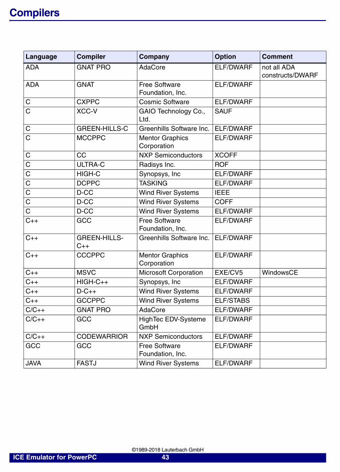
Compilers
Language Compiler Company Option Comment
ADA GNAT PRO AdaCore ELF/DWARF not all ADA constructs/DWARF
ADA GNAT Free Software Foundation, Inc.
ELF/DWARF
C CXPPC Cosmic Software ELF/DWARFC XCC-V GAIO Technology Co.,
Ltd.SAUF
C GREEN-HILLS-C Greenhills Software Inc. ELF/DWARFC MCCPPC Mentor Graphics
CorporationELF/DWARF
C CC NXP Semiconductors XCOFFC ULTRA-C Radisys Inc. ROFC HIGH-C Synopsys, Inc ELF/DWARFC DCPPC TASKING ELF/DWARFC D-CC Wind River Systems IEEEC D-CC Wind River Systems COFFC D-CC Wind River Systems ELF/DWARFC++ GCC Free Software
Foundation, Inc.ELF/DWARF
C++ GREEN-HILLS-C++
Greenhills Software Inc. ELF/DWARF
C++ CCCPPC Mentor Graphics Corporation
ELF/DWARF
C++ MSVC Microsoft Corporation EXE/CV5 WindowsCEC++ HIGH-C++ Synopsys, Inc ELF/DWARFC++ D-C++ Wind River Systems ELF/DWARFC++ GCCPPC Wind River Systems ELF/STABSC/C++ GNAT PRO AdaCore ELF/DWARFC/C++ GCC HighTec EDV-Systeme
GmbHELF/DWARF
C/C++ CODEWARRIOR NXP Semiconductors ELF/DWARFGCC GCC Free Software
Foundation, Inc.ELF/DWARF
JAVA FASTJ Wind River Systems ELF/DWARF
ICE Emulator for PowerPC 43 ©1989-2018 Lauterbach GmbH

3rd Party Tool Integrations
CPU Tool Company Host
WINDOWS CE PLATF. BUILDER
- Windows
CODE::BLOCKS - -C++TEST - WindowsADENEO -X-TOOLS / X32 blue river software GmbH WindowsCODEWRIGHT Borland Software
CorporationWindows
CODE CONFIDENCE TOOLS
Code Confidence Ltd Windows
CODE CONFIDENCE TOOLS
Code Confidence Ltd Linux
EASYCODE EASYCODE GmbH WindowsECLIPSE Eclipse Foundation, Inc WindowsCHRONVIEW Inchron GmbH WindowsLDRA TOOL SUITE LDRA Technology, Inc. WindowsUML DEBUGGER LieberLieber Software
GmbHWindows
SIMULINK The MathWorks Inc. WindowsATTOL TOOLS MicroMax Inc. WindowsVISUAL BASIC INTERFACE
Microsoft Corporation Windows
LABVIEW NATIONAL INSTRUMENTS Corporation
Windows
TPT PikeTec GmbH WindowsCANTATA QA Systems Ltd WindowsRAPITIME Rapita Systems Ltd. WindowsRHAPSODY IN MICROC IBM Corp. WindowsRHAPSODY IN C++ IBM Corp. WindowsDA-C RistanCASE WindowsTRACEANALYZER Symtavision GmbH WindowsECU-TEST TraceTronic GmbH WindowsUNDODB Undo Software LinuxTA INSPECTOR Vector WindowsVECTORCAST UNIT TESTING
Vector Software Windows
VECTORCAST CODE COVERAGE
Vector Software Windows
POWERPC OSE ILLUMINATOR Enea OSE Systems WindowsPOWERPC DIAB RTA SUITE Wind River Systems Windows
ICE Emulator for PowerPC 44 ©1989-2018 Lauterbach GmbH

Realtime operation Systems
Company Product Comment
KadakProducts Ltd. AMXOracle Corporation ChorusOSCMX Systems Inc. CMX-RTXDDC-I, Inc. DEOS implemented by DDC-IElektrobit Automotive GmbH
EB tresos AutoCore OS via ORTI
Elektrobit Automotive GmbH
EB tresos Safety OS via ORTI
eCosCentric Limited ECOS 1.3, 2.0 and 3.0ETAS GmbH ERCOSEK via ORTIEvidence Erika via ORTIfreeRTOS FreeRTOS up to v9HIPPEROS S.A. HIPPEROS implemented by HIPPEROS- Linux Kernel Version 2.4 and 2.6, 3.x, 4.xMontaVista Software, LLC Linux 3.0, 3.1, 4.0, 5.0LynuxWorks Inc. LynxOS 3.1.0, 3.1.0a, 4.0NXP Semiconductors MQX 3.x and 4.xSynopsys, Inc MQX 2.40 and 2.50- NetBSDMISPO Co. Ltd. NORTiMentor Graphics Corporation
Nucleus PLUS
Radisys Inc. OS-9Enea OSE Systems OSE Delta 4.x and 5.x- OSEK via ORTINXP Semiconductors OSEKturbo via ORTI/former MetrowerksOSEKSysgo AG PikeOS up to 4.2.1Elektrobit Automotive GmbH
ProOSEK via ORTI
Wind River Systems pSOS+ 2.1 to 2.5, 3.0, with TRACE32QNX Software Systems QNX 6.0 to 7.0RTEMS RTEMS up to v5Quadros Systems Inc. RTXC 3.2Quadros Systems Inc. RTXC QuadrosSciopta ScioptaMicro Digital Inc. SMX 3.4 to 4.3
ICE Emulator for PowerPC 45 ©1989-2018 Lauterbach GmbH

Express Logic Inc. ThreadX 3.0, 4.0, 5.0Micrium Inc. uC/OS-II 2.0 to 2.92- uITRON HI7000, RX4000, NORTi,PrKernelMentor Graphics Corporation
VRTXsa
Wind River Systems VxWorks 5.x to 7.x
Company Product Comment
ICE Emulator for PowerPC 46 ©1989-2018 Lauterbach GmbH

Emulation Modules
Module Overview
tbd
ICE Emulator for PowerPC 47 ©1989-2018 Lauterbach GmbH

Order Information
Order No. Code Text
AI-7206 BGA272-EXTENSION BGA272-Adapter ExtensionAI-7207 BGA357-AI-MALE Advanced Interconnect male-male-block for MPCAI-7208 BGA357-AI-SOCKET Advanced Interconnect socket for MPC860/880AI-7209 BGA357-EXTENSION BGA357-Adapter ExtensionAI-9546 BGA256-AI-SOCKET Advanced Interconnect socket for MPC850AI-9549 BGA272-AI-SOCKET Advanced Interconnect socket for MPC555AI-9664 BGA388-AI-SOCKET Advanced Interconnect socket for MPC561/563 AAI-9667 BGA388-ADAPTER Advanced Interconnect BGA388 Adapter for CPUAI-9672 BGA388-MALE-MALE-28 BGA388 Male-Male Connector 0.28mm PinAI-9673 BGA388-MALE-MALE-22 BGA388 Male-Male Connector 0.20mm PinLA-7210 BGA357-ETEC-MPC860 Emulation adapter for E-TEC socket for MPC860LA-7211 CONNECTOR-ADS-MPC860 Emulation adapter for ADS boardLA-7213 BGA357-AI-MPC860 Emulation adapter for AI socket for MPC860LA-7214 BGA357-ETEC-SOCKET E-TEC socket for MPC860 (SMD)LA-7215 A-MPC860-BOTTOM Bottom Side Target Adapter for MPC860LA-7217 CON.-FADS-MPC860 Emulation adapter for FADS boardLA-7218 BGA357-ETEC-SOCKET-T E-TEC socket for MPC860 (through hole)LA-7907 TCON320-BGA357-PPC Emulation adap. f. TCON320 to BGA357-MPC880LA-9545 BGA256-AI-MPC850/PPC Emulation adapter for AI socket for MPC850LA-9548 BGA272-AI-MPC555 Emulation adapter for AI socket for MPC555LA-9660 TCON200-MPC823-AMC Converter TCON 200 to AMC Footprint 823LA-9661 TCON240-AI-MPC555 Emulation adap. from TCON240 to BGA272-MPC555LA-9666 TCON320-AI-MPC56X Emulation adap. from TCON320 to BGA388-MPC56x
Additional OptionsLA-7216 BGA357-CPU-ADAPTER CPU Test Adapter for BGA357 (MPC860)
ICE Emulator for PowerPC 48 ©1989-2018 Lauterbach GmbH

Operating Voltage
tbd
ICE Emulator for PowerPC 49 ©1989-2018 Lauterbach GmbH

Physical Dimensions
Dimension
LA-7221 M-PPC403GA-QFP
cable (400)
94
37
15
133141
SIDE VIEW
15
8
82
TOP VIEW (all dimensions in mm)
9
7
1
ICE Emulator for PowerPC 50 ©1989-2018 Lauterbach GmbH

LA-7222 M-PPC403GB-QFP
Dimension
cable (400)
98
37
15
136143
SIDE VIEW
15
8
74
TOP VIEW (all dimensions in mm)
7
3
1
ICE Emulator for PowerPC 51 ©1989-2018 Lauterbach GmbH

LA-7203 M-MPC505-QFP
Dimension
cable (400)
94
37
15
133141
SIDE VIEW
15
8
82
TOP VIEW (all dimensions in mm)
9
7
1
ICE Emulator for PowerPC 52 ©1989-2018 Lauterbach GmbH
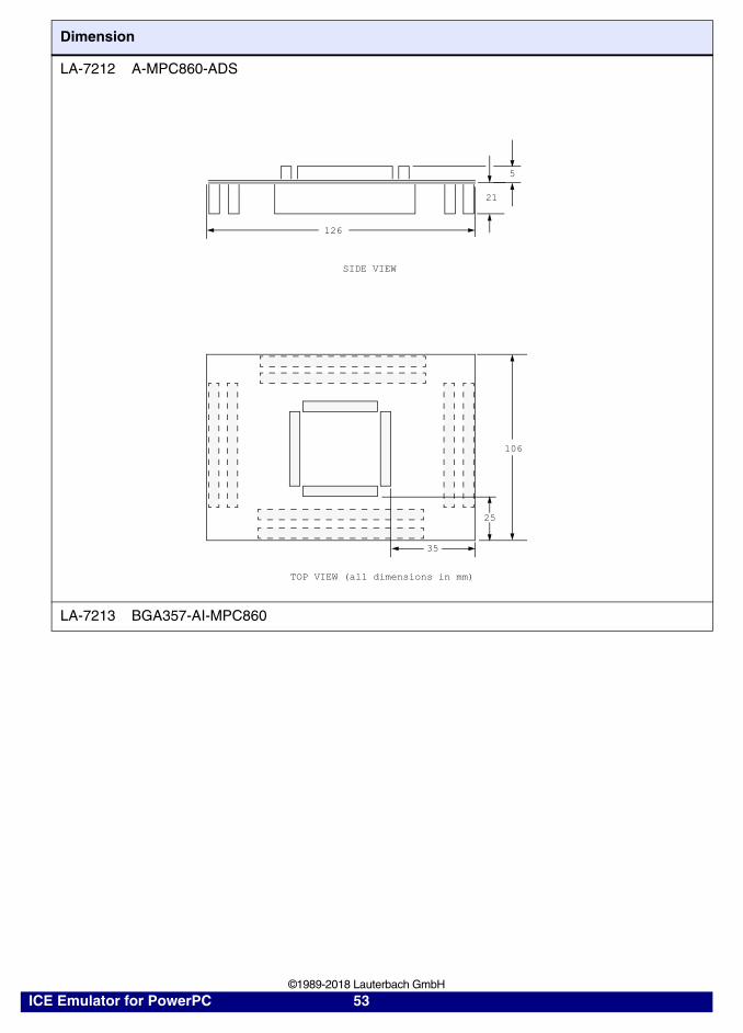
LA-7212 A-MPC860-ADS
LA-7213 BGA357-AI-MPC860
Dimension
126
SIDE VIEW
5
21
TOP VIEW (all dimensions in mm)
25
35
106
ICE Emulator for PowerPC 53 ©1989-2018 Lauterbach GmbH
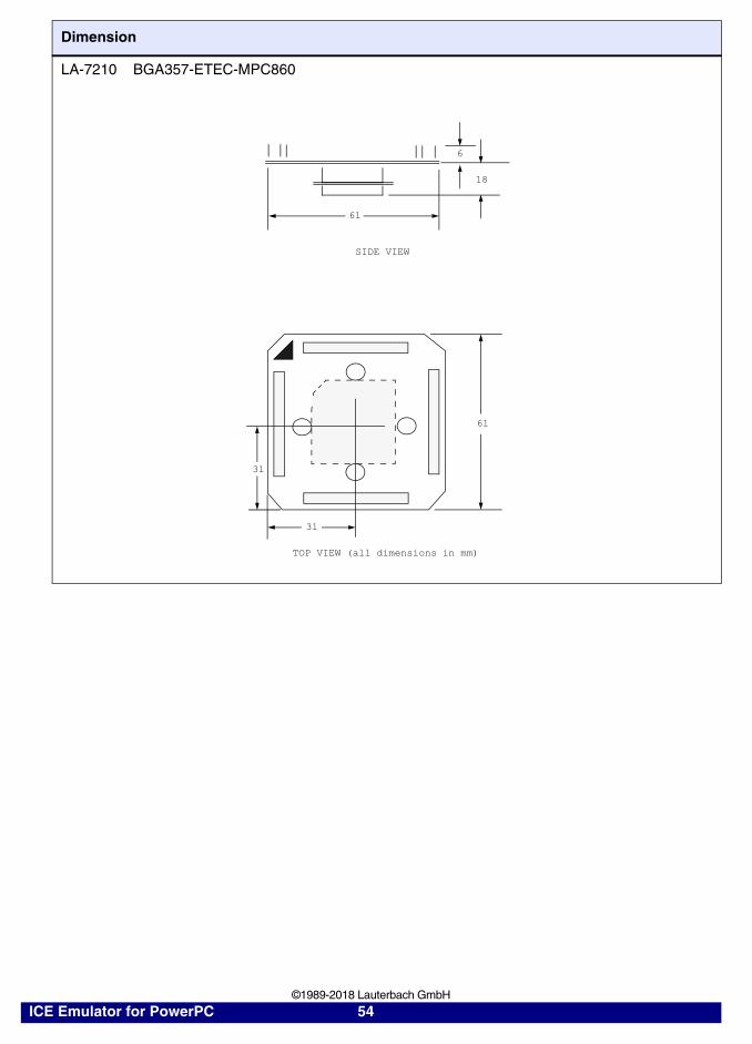
LA-7210 BGA357-ETEC-MPC860
Dimension
18
61
SIDE VIEW
6
61
31
31
TOP VIEW (all dimensions in mm)
ICE Emulator for PowerPC 54 ©1989-2018 Lauterbach GmbH

LA-9539 BGA272-CPU-ADAPTER
LA-9548 BGA272-AI-MPC555
Dimension
2400
2000
4x100
50
425
180
SAMTEC:TFM-130-32-S-D-LC
SAMTEC:SFM-130-L1-S-D-LC
SIDE VIEW
ALL DIMENSIONS IN 1/1000 INCH
TOP VIEW
1
TOP VIEW
SIDE VIEWSAMTEC:TFM-130-32-S-D-LC
ALL DIMENSIONS IN 1/1000 INCH
500
425
50
4X100
240
020
00
1
ICE Emulator for PowerPC 55 ©1989-2018 Lauterbach GmbH

LA-7907 TCON320-BGA357-PPC
Dimension
TOP VIEW
SIDE VIEW
ALL DIMENSIONS IN 1/1000 INCH
PIN1
1425
2850
300
50010
50
SAMTEC: TFM-140-32-S-D-LC
142
5
285
0
BGA ADAPTERSYSTEM
(ADVANCED)SOLDER IN
OOOOOOOOOOOOOOO
ICE Emulator for PowerPC 56 ©1989-2018 Lauterbach GmbH

Adapter
Not necessary.
ICE Emulator for PowerPC 57 ©1989-2018 Lauterbach GmbH
Related Documents