1. General description The LPC2939 combine an ARM968E-S CPU core with two integrated TCM blocks operating at frequencies of up to 125 MHz, Full-speed USB 2.0 Host/OTG/Device controller, CAN and LIN, 56 kB SRAM, 768 kB flash memory, external memory interface, three 10-bit ADCs, and multiple serial and parallel interfaces in a single chip targeted at consumer, industrial, medical, and communication markets. To optimize system power consumption, the LPC2939 has a very flexible Clock Generation Unit (CGU) that provides dynamic clock gating and scaling. 2. Features and benefits ARM968E-S processor running at frequencies of up to 125 MHz maximum. Multilayer AHB system bus at 125 MHz with four separate layers. On-chip memory: Two Tightly Coupled Memories (TCM), 32 kB Instruction (ITCM), 32 kB Data TCM (DTCM) Two separate internal Static RAM (SRAM) instances; 32 kB SRAM and 16 kB SRAM 8 kB ETB SRAM, also usable for code execution and data 768 kB high-speed flash program memory 16 kB true EEPROM, byte-erasable/programmable Dual-master, eight-channel GPDMA controller on the AHB multilayer matrix which can be used with the SPI interfaces and the UARTs, as well as for memory-to-memory transfers including the TCM memories External Static Memory Controller (SMC) with eight memory banks; up to 32-bit data bus; up to 24-bit address bus Serial interfaces: USB 2.0 full-speed Host/OTG/Device controller with dedicated DMA controller and on-chip device PHY Two-channel CAN controller supporting FullCAN and extensive message filtering Two LIN master controllers with full hardware support for LIN communication. The LIN interface can be configured as UART to provide two additional UART interfaces. Two 550 UARTs with 16-byte Tx and Rx FIFO depths, DMA support, modem control, and RS-485/EIA-485 (9-bit) support Three full-duplex Q-SPIs with four slave-select lines; 16 bits wide; 8 locations deep; Tx FIFO and Rx FIFO Two I 2 C-bus interfaces LPC2939 ARM9 microcontroller with CAN, LIN, and USB Rev. 03 — 7 April 2010 Product data sheet

Welcome message from author
This document is posted to help you gain knowledge. Please leave a comment to let me know what you think about it! Share it to your friends and learn new things together.
Transcript
1. General description
The LPC2939 combine an ARM968E-S CPU core with two integrated TCM blocks operating at frequencies of up to 125 MHz, Full-speed USB 2.0 Host/OTG/Device controller, CAN and LIN, 56 kB SRAM, 768 kB flash memory, external memory interface, three 10-bit ADCs, and multiple serial and parallel interfaces in a single chip targeted at consumer, industrial, medical, and communication markets. To optimize system power consumption, the LPC2939 has a very flexible Clock Generation Unit (CGU) that provides dynamic clock gating and scaling.
2. Features and benefits
ARM968E-S processor running at frequencies of up to 125 MHz maximum.
Multilayer AHB system bus at 125 MHz with four separate layers.
On-chip memory:
Two Tightly Coupled Memories (TCM), 32 kB Instruction (ITCM), 32 kB Data TCM (DTCM)
Two separate internal Static RAM (SRAM) instances; 32 kB SRAM and 16 kB SRAM
8 kB ETB SRAM, also usable for code execution and data
768 kB high-speed flash program memory
16 kB true EEPROM, byte-erasable/programmable
Dual-master, eight-channel GPDMA controller on the AHB multilayer matrix which can be used with the SPI interfaces and the UARTs, as well as for memory-to-memory transfers including the TCM memories
External Static Memory Controller (SMC) with eight memory banks; up to 32-bit data bus; up to 24-bit address bus
Serial interfaces:
USB 2.0 full-speed Host/OTG/Device controller with dedicated DMA controller and on-chip device PHY
Two-channel CAN controller supporting FullCAN and extensive message filtering
Two LIN master controllers with full hardware support for LIN communication. The LIN interface can be configured as UART to provide two additional UART interfaces.
Two 550 UARTs with 16-byte Tx and Rx FIFO depths, DMA support, modem control, and RS-485/EIA-485 (9-bit) support
Three full-duplex Q-SPIs with four slave-select lines; 16 bits wide; 8 locations deep; Tx FIFO and Rx FIFO
Two I2C-bus interfaces
LPC2939ARM9 microcontroller with CAN, LIN, and USBRev. 03 — 7 April 2010 Product data sheet
NXP Semiconductors LPC2939ARM9 microcontroller with CAN, LIN, and USB
Other peripherals:
One 10-bit ADC with 5.0 V measurement range and eight input channels with conversion times as low as 2.44 s per channel
Two 10-bit ADCs, 8-channels each, with 3.3 V measurement range provide an additional 16 analog inputs with conversion times as low as 2.44 s per channel. Each channel provides a compare function to minimize interrupts.
Multiple trigger-start option for all ADCs: timer, PWM, other ADC, and external signal input
Four 32-bit timers each containing four capture-and-compare registers linked to I/Os
Four six-channel PWMs (Pulse-Width Modulators) with capture and trap functionality
Two dedicated 32-bit timers to schedule and synchronize PWM and ADC
Quadrature encoder interface that can monitor one external quadrature encoder
32-bit watchdog with timer change protection, running on safe clock
Up to 152 general-purpose I/O pins with programmable pull-up, pull-down, or bus keeper
Vectored Interrupt Controller (VIC) with 16 priority levels
Up to 22 level-sensitive external interrupt pins, including USB, CAN and LIN wake-up features
Configurable clock-out pin for driving external system clocks
Processor wake-up from power-down via external interrupt pins and CAN or LIN activity
Flexible Reset Generator Unit (RGU) able to control resets of individual modules
Flexible Clock-Generation Unit (CGU) able to control clock frequency of individual modules:
On-chip very low-power ring oscillator; fixed frequency of 0.4 MHz; always on to provide a Safe_Clock source for system monitoring
On-chip crystal oscillator with a recommended operating range from 10 MHz to 25 MHz. PLL input range 10 MHz to 25 MHz.
On-chip PLL allows CPU operation up to a maximum CPU rate of 125 MHz
Generation of up to 11 base clocks
Seven fractional dividers
Second, dedicated CGU with its own PLL generates USB clocks and a configurable clock output
Highly configurable system Power Management Unit (PMU):
clock control of individual modules
allows minimization of system operating power consumption in any configuration
Standard ARM test and debug interface with real-time in-circuit emulator
Boundary-scan test supported
ETM/ETB debug functions with 8 kB of dedicated SRAM also accessible for application code and data storage
Dual power supply:
CPU operating voltage: 1.8 V 5 %
I/O operating voltage: 2.7 V to 3.6 V; inputs tolerant up to 5.5 V
208-pin LQFP package
LPC2939_3 All information provided in this document is subject to legal disclaimers. © NXP B.V. 2010. All rights reserved.
Product data sheet Rev. 03 — 7 April 2010 2 of 99
NXP Semiconductors LPC2939ARM9 microcontroller with CAN, LIN, and USB
40 C to +85 C ambient operating temperature range
3. Ordering information
3.1 Ordering options
Table 1. Ordering information
Type number Package
Name Description Version
LPC2939FBD208 LQFP208 plastic low profile quad flat package; 208 leads; body 28 x 28 x 1.4 mm SOT459-1
Table 2. Part options
Type number Flash memory
SRAM SMC USB Host/OTG/device
UART RS-485/modem
LIN 2.0/UART
CAN Package
LPC2939FBD208 768 kB 56 kB + 2 32 kB TCM
32-bit yes 2 2 2 LQFP208
LPC2939_3 All information provided in this document is subject to legal disclaimers. © NXP B.V. 2010. All rights reserved.
Product data sheet Rev. 03 — 7 April 2010 3 of 99
NXP Semiconductors LPC2939ARM9 microcontroller with CAN, LIN, and USB
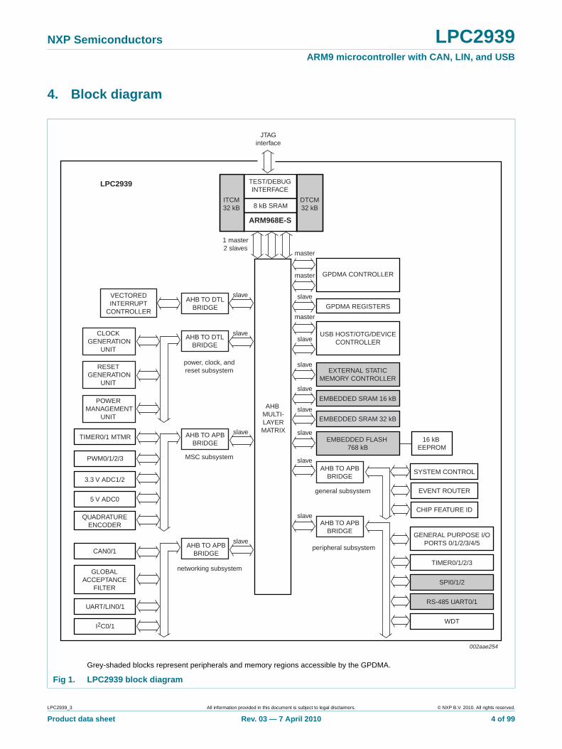
4. Block diagram
Grey-shaded blocks represent peripherals and memory regions accessible by the GPDMA.
Fig 1. LPC2939 block diagram
002aae254
ARM968E-S
DTCM32 kB
ITCM32 kB
TEST/DEBUGINTERFACE
slave
master
1 master2 slaves
master
EXTERNAL STATICMEMORY CONTROLLER
GPDMA CONTROLLER
GPDMA REGISTERS
EMBEDDED FLASH 768 kB
16 kB EEPROM
EMBEDDED SRAM 32 kB
SYSTEM CONTROL
TIMER0/1 MTMR
CAN0/1
GLOBALACCEPTANCE
FILTER
UART/LIN0/1
PWM0/1/2/3
3.3 V ADC1/2
EVENT ROUTER
EMBEDDED SRAM 16 kB
GENERAL PURPOSE I/OPORTS 0/1/2/3/4/5
TIMER0/1/2/3
SPI0/1/2
RS-485 UART0/1
WDT
AHB TO APBBRIDGE
AHB TO DTLBRIDGE
VECTOREDINTERRUPT
CONTROLLERmaster
slaveUSB HOST/OTG/DEVICE
CONTROLLER
slave
slave
slave
slave
slave
slave
slave
slave
slave
slave
AHB TO DTLBRIDGE
AHB TO APBBRIDGE
5 V ADC0
QUADRATUREENCODER
CHIP FEATURE ID
AHB TO APBBRIDGE
I2C0/1
AHB TO APBBRIDGE
CLOCK GENERATION
UNIT
POWER MANAGEMENT
UNIT
RESET GENERATION
UNIT
AHB MULTI-LAYERMATRIX
LPC2939
JTAGinterface
8 kB SRAM
general subsystem
power, clock, andreset subsystem
MSC subsystem
networking subsystem
peripheral subsystem
LPC2939_3 All information provided in this document is subject to legal disclaimers. © NXP B.V. 2010. All rights reserved.
Product data sheet Rev. 03 — 7 April 2010 4 of 99
NXP Semiconductors LPC2939ARM9 microcontroller with CAN, LIN, and USB
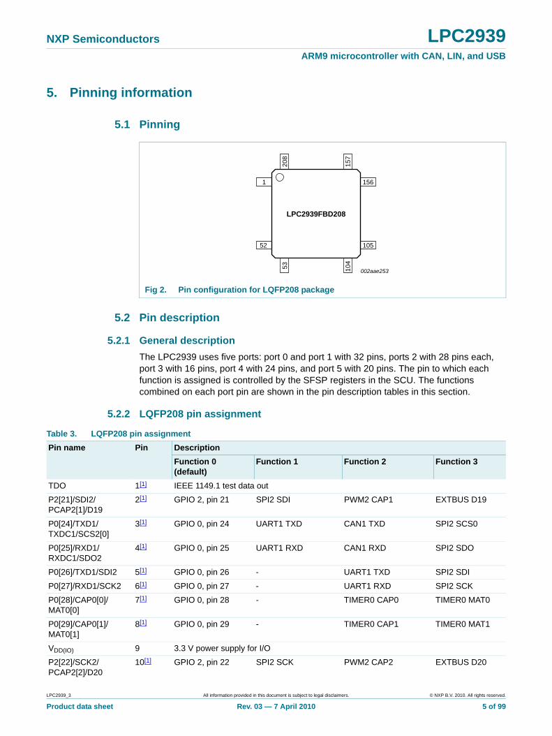
5. Pinning information
5.1 Pinning
5.2 Pin description
5.2.1 General description
The LPC2939 uses five ports: port 0 and port 1 with 32 pins, ports 2 with 28 pins each, port 3 with 16 pins, port 4 with 24 pins, and port 5 with 20 pins. The pin to which each function is assigned is controlled by the SFSP registers in the SCU. The functions combined on each port pin are shown in the pin description tables in this section.
5.2.2 LQFP208 pin assignment
Fig 2. Pin configuration for LQFP208 package
LPC2939FBD208
156
53 104
208
157
105
1
52
002aae253
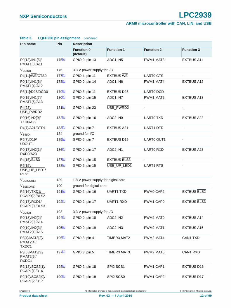
Table 3. LQFP208 pin assignment
Pin name Pin Description
Function 0 (default)
Function 1 Function 2 Function 3
TDO 1[1] IEEE 1149.1 test data out
P2[21]/SDI2/PCAP2[1]/D19
2[1] GPIO 2, pin 21 SPI2 SDI PWM2 CAP1 EXTBUS D19
P0[24]/TXD1/TXDC1/SCS2[0]
3[1] GPIO 0, pin 24 UART1 TXD CAN1 TXD SPI2 SCS0
P0[25]/RXD1/RXDC1/SDO2
4[1] GPIO 0, pin 25 UART1 RXD CAN1 RXD SPI2 SDO
P0[26]/TXD1/SDI2 5[1] GPIO 0, pin 26 - UART1 TXD SPI2 SDI
P0[27]/RXD1/SCK2 6[1] GPIO 0, pin 27 - UART1 RXD SPI2 SCK
P0[28]/CAP0[0]/MAT0[0]
7[1] GPIO 0, pin 28 - TIMER0 CAP0 TIMER0 MAT0
P0[29]/CAP0[1]/MAT0[1]
8[1] GPIO 0, pin 29 - TIMER0 CAP1 TIMER0 MAT1
VDD(IO) 9 3.3 V power supply for I/O
P2[22]/SCK2/PCAP2[2]/D20
10[1] GPIO 2, pin 22 SPI2 SCK PWM2 CAP2 EXTBUS D20
LPC2939_3 All information provided in this document is subject to legal disclaimers. © NXP B.V. 2010. All rights reserved.
Product data sheet Rev. 03 — 7 April 2010 5 of 99
NXP Semiconductors LPC2939ARM9 microcontroller with CAN, LIN, and USB
P2[23]/SCS1[0]/PCAP3[0]/D21
11[1] GPIO 2, pin 23 SPI1 SCS0 PWM3 CAP0 EXTBUS D21
P3[6]/SCS0[3]/PMAT1[0]/TXDL1
12[1] GPIO 3, pin 6 SPI0 SCS3 PWM1 MAT0 LIN1/UART TXD
P3[7]/SCS2[1]/PMAT1[1]/RXDL1
13[1] GPIO 3, pin 7 SPI2 SCS1 PWM1 MAT1 LIN1/UART RXD
P0[30]/CAP0[2]/MAT0[2]
14[1] GPIO 0, pin 30 - TIMER0 CAP2 TIMER0 MAT2
P0[31]/CAP0[3]/MAT0[3]
15[1] GPIO 0, pin 31 - TIMER0 CAP3 TIMER0 MAT3
P2[24]/SCS1[1]/PCAP3[1]/D22
16[1] GPIO 2, pin 24 SPI1 SCS1 PWM3 CAP1 EXTBUS D22
P2[25]/SCS1[2]/PCAP3[2]/D23
17[1] GPIO 2, pin 25 SPI1 SCS2 PWM3 CAP2 EXTBUS D23
VSS(IO) 18 ground for I/O
P5[19]/USB_D+1 19[2] GPIO 5, pin 19 USB_D+1 - -
P5[18]/USB_D1 20[2] GPIO 5, pin 18 USB_D1 - -
P5[17]/USB_D+2 21[2] GPIO 5, pin 17 USB_D+2 - -
P5[16]/USB_D2 22[2] GPIO 5, pin 16 USB_D2 - -
VDD(IO) 23 3.3 V power supply for I/O
VDD(CORE) 24 1.8 V power supply for digital core
VSS(CORE) 25 ground for core
P1[31]/CAP0[1]/MAT0[1]/EI5
26[1] GPIO 1, pin 31 TIMER0 CAP1 TIMER0 MAT1 EXTINT5
VSS(IO) 27 ground for I/O
P4[0]/A8 28[1] GPIO 4, pin 0 EXTBUS A8 - -
P1[30]/CAP0[0]/MAT0[0]/EI4
29[1] GPIO 1, pin 30 TIMER0 CAP0 TIMER0 MAT0 EXTINT4
P5[0]/D8 30[1] GPIO 5, pin 0 EXTBUS D8 - -
P3[8]/SCS2[0]/PMAT1[2]/USB_OVRCR1
31[1] GPIO 3, pin 8 SPI2 SCS0 PWM1 MAT2 USB_OVRCR1
P3[9]/SDO2/PMAT1[3]/USB_PPWR1
32[1] GPIO 3, pin 9 SPI2 SDO PWM1 MAT3 USB_PPWR1
P1[29]/CAP1[0]/ TRAP0/ PMAT3[5]
33[1] GPIO 1, pin 29 TIMER1 CAP0/ADC0 EXTSTART
PWM TRAP0 PWM3 MAT5
VDD(IO) 34 3.3 V power supply for I/O
P4[16]/CS6/U1OUT1
35[1] GPIO 4, pin 16 EXTBUS CS6 UART1 OUT1 -
P1[28]/CAP1[1]/TRAP1/PMAT3[4]
36[1] GPIO 1, pin 28 TIMER1 CAP1/ADC1 EXTSTART
PWM TRAP1 PWM3 MAT4
P2[26]/CAP0[2]/MAT0[2]/EI6
37[1] GPIO 2, pin 26 TIMER0 CAP2 TIMER0 MAT2 EXTINT6
Table 3. LQFP208 pin assignment …continued
Pin name Pin Description
Function 0 (default)
Function 1 Function 2 Function 3
LPC2939_3 All information provided in this document is subject to legal disclaimers. © NXP B.V. 2010. All rights reserved.
Product data sheet Rev. 03 — 7 April 2010 6 of 99
NXP Semiconductors LPC2939ARM9 microcontroller with CAN, LIN, and USB
P4[8]/A22/DSR1 38 GPIO 4, pin 8 EXTBUS A22 UART1 DSR -
VSS(IO) 39 ground for I/O
P2[27]/CAP0[3]/MAT0[3]/EI7
40[1] GPIO 2, pin 27 TIMER0 CAP3 TIMER0 MAT3 EXTINT7
P5[8]/D20/U0OUT2 41[1] GPIO 5, pin 8 EXTBUS D20 UART0 OUT2 -
P1[27]/CAP1[2]/TRAP2/PMAT3[3]
42[1] GPIO 1, pin 27 TIMER1 CAP2, ADC2 EXTSTART
PWM TRAP2 PWM3 MAT3
P1[26]/PMAT2[0]/TRAP3/PMAT3[2]
43[1] GPIO 1, pin 26 PWM2 MAT0 PWM TRAP3 PWM3 MAT2
P4[20]/USB_VBUS2
44[1] GPIO 4, pin 20 USB_VBUS2 - -
VDD(IO) 45 3.3 V power supply for I/O
P1[25]/PMAT1[0]/USB_VBUS1/PMAT3[1]
46[1] GPIO 1, pin 25 PWM1 MAT0 USB_VBUS1 PWM3 MAT1
VSS(CORE) 47 ground for core
VDD(CORE) 48 1.8 V power supply for digital core
P1[24]/PMAT0[0]/USB_CONNECT1/PMAT3[0]
49[1] GPIO 1, pin 24 PWM0 MAT0 USB_CONNECT1 PWM3 MAT0
P1[23]/RXD0/USB_SSPND1/CS5
50[1] GPIO 1, pin 23 UART0 RXD USB_SSPND1 EXTBUS CS5
P1[22]/TXD0/USB_UP_LED1/CS4
51[1] GPIO 1, pin 22 UART0 TXD USB_UP_LED1 EXTBUS CS4
TMS 52[1] IEEE 1149.1 test mode select, pulled up internally
TCK 53[1] IEEE 1149.1 test clock
P1[21]/CAP3[3]/CAP1[3]/D7
54[1] GPIO 1, pin 21 TIMER3 CAP3 TIMER1 CAP3, MSCSS PAUSE
EXTBUS D7
P1[20]/CAP3[2]/SCS0[1]/D6
55[1] GPIO 1, pin 20 TIMER3 CAP2 SPI0 SCS1 EXTBUS D6
P1[19]/CAP3[1]/SCS0[2]/D5
56[1] GPIO 1, pin 19 TIMER3 CAP1 SPI0 SCS2 EXTBUS D5
P1[18]/CAP3[0]/SDO0/D4
57[1] GPIO 1, pin 18 TIMER3 CAP0 SPI0 SDO EXTBUS D4
P1[17]/CAP2[3]/SDI0/D3
58[1] GPIO 1, pin 17 TIMER2 CAP3 SPI0 SDI EXTBUS D3
VSS(IO) 59 ground for I/O
P4[4]/A12 60[1] GPIO 4, pin 4 EXTBUS A12 - -
P1[16]/CAP2[2]/SCK0/D2
61[1] GPIO 1, pin 16 TIMER2 CAP2 SPI0 SCK EXTBUS D2
P5[4]/D16 62[1] GPIO 5, pin 4 EXTBUS D16 - -
P2[0]/MAT2[0]/TRAP3/D8
63[1] GPIO 2, pin 0 TIMER2 MAT0 PWM TRAP3 EXTBUS D8
Table 3. LQFP208 pin assignment …continued
Pin name Pin Description
Function 0 (default)
Function 1 Function 2 Function 3
LPC2939_3 All information provided in this document is subject to legal disclaimers. © NXP B.V. 2010. All rights reserved.
Product data sheet Rev. 03 — 7 April 2010 7 of 99
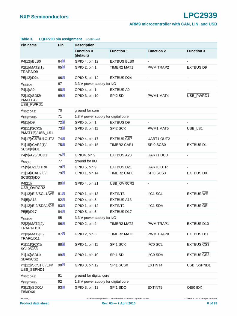
NXP Semiconductors LPC2939ARM9 microcontroller with CAN, LIN, and USB
P4[12]/BLS0 64[1] GPIO 4, pin 12 EXTBUS BLS0 - -
P2[1]/MAT2[1]/TRAP2/D9
65[1] GPIO 2, pin 1 TIMER2 MAT1 PWM TRAP2 EXTBUS D9
P5[12]/D24 66[1] GPIO 5, pin 12 EXTBUS D24 - -
VDD(IO) 67 3.3 V power supply for I/O
P4[1]/A9 68[1] GPIO 4, pin 1 EXTBUS A9 - -
P3[10]/SDI2/PMAT1[4]/USB_PWRD1
69[1] GPIO 3, pin 10 SPI2 SDI PWM1 MAT4 USB_PWRD1
VSS(CORE) 70 ground for core
VDD(CORE) 71 1.8 V power supply for digital core
P5[1]/D9 72[1] GPIO 5, pin 1 EXTBUS D9 - -
P3[11]/SCK2/PMAT1[5]/USB_LS1
73[1] GPIO 3, pin 11 SPI2 SCK PWM1 MAT5 USB_LS1
P4[17]/CS7/U1OUT2 74[1] GPIO 4, pin 17 EXTBUS CS7 UART1 OUT2 -
P1[15]/CAP2[1]/SCS0[0]/D1
75[1] GPIO 1, pin 15 TIMER2 CAP1 SPI0 SCS0 EXTBUS D1
P4[9]/A23/DCD1 76[1] GPIO4, pin 9 EXTBUS A23 UART1 DCD -
VSS(IO) 77 ground for I/O
P5[9]/D21/DTR0 78[1] GPIO 5, pin 9 EXTBUS D21 UART0 DTR -
P1[14]/CAP2[0]/SCS0[3]/D0
79[1] GPIO 1, pin 14 TIMER2 CAP0 SPI0 SCS3 EXTBUS D0
P4[21]/USB_OVRCR2
80[1] GPIO 4, pin 21 USB_OVRCR2 - -
P1[13]/EI3/SCL1/WE 81[1] GPIO 1, pin 13 EXTINT3 I2C1 SCL EXTBUS WE
P4[5]/A13 82[1] GPIO 4, pin 5 EXTBUS A13 - -
P1[12]/EI2/SDA1/OE 83[1] GPIO 1, pin 12 EXTINT2 I2C1 SDA EXTBUS OE
P5[5]/D17 84[1] GPIO 5, pin 5 EXTBUS D17 - -
VDD(IO) 85 3.3 V power supply for I/O
P2[2]/MAT2[2]/TRAP1/D10
86[1] GPIO 2, pin 2 TIMER2 MAT2 PWM TRAP1 EXTBUS D10
P2[3]/MAT2[3]/TRAP0/D11
87[1] GPIO 2, pin 3 TIMER2 MAT3 PWM TRAP0 EXTBUS D11
P1[11]/SCK1/SCL0/CS3
88[1] GPIO 1, pin 11 SPI1 SCK I2C0 SCL EXTBUS CS3
P1[10]/SDI1/SDA0/CS2
89[1] GPIO 1, pin 10 SPI1 SDI I2C0 SDA EXTBUS CS2
P3[12]/SCS1[0]/EI4/USB_SSPND1
90[1] GPIO 3, pin 12 SPI1 SCS0 EXTINT4 USB_SSPND1
VSS(CORE) 91 ground for digital core
VDD(CORE) 92 1.8 V power supply for digital core
P3[13]/SDO1/EI5/IDX0
93[1] GPIO 3, pin 13 SPI1 SDO EXTINT5 QEI0 IDX
Table 3. LQFP208 pin assignment …continued
Pin name Pin Description
Function 0 (default)
Function 1 Function 2 Function 3
LPC2939_3 All information provided in this document is subject to legal disclaimers. © NXP B.V. 2010. All rights reserved.
Product data sheet Rev. 03 — 7 April 2010 8 of 99
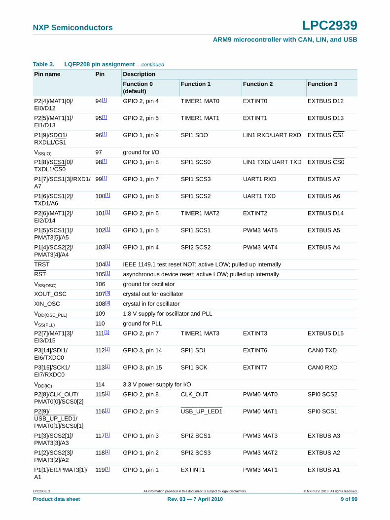
NXP Semiconductors LPC2939ARM9 microcontroller with CAN, LIN, and USB
P2[4]/MAT1[0]/EI0/D12
94[1] GPIO 2, pin 4 TIMER1 MAT0 EXTINT0 EXTBUS D12
P2[5]/MAT1[1]/EI1/D13
95[1] GPIO 2, pin 5 TIMER1 MAT1 EXTINT1 EXTBUS D13
P1[9]/SDO1/RXDL1/CS1
96[1] GPIO 1, pin 9 SPI1 SDO LIN1 RXD/UART RXD EXTBUS CS1
VSS(IO) 97 ground for I/O
P1[8]/SCS1[0]/TXDL1/CS0
98[1] GPIO 1, pin 8 SPI1 SCS0 LIN1 TXD/ UART TXD EXTBUS CS0
P1[7]/SCS1[3]/RXD1/A7
99[1] GPIO 1, pin 7 SPI1 SCS3 UART1 RXD EXTBUS A7
P1[6]/SCS1[2]/TXD1/A6
100[1] GPIO 1, pin 6 SPI1 SCS2 UART1 TXD EXTBUS A6
P2[6]/MAT1[2]/EI2/D14
101[1] GPIO 2, pin 6 TIMER1 MAT2 EXTINT2 EXTBUS D14
P1[5]/SCS1[1]/PMAT3[5]/A5
102[1] GPIO 1, pin 5 SPI1 SCS1 PWM3 MAT5 EXTBUS A5
P1[4]/SCS2[2]/PMAT3[4]/A4
103[1] GPIO 1, pin 4 SPI2 SCS2 PWM3 MAT4 EXTBUS A4
TRST 104[1] IEEE 1149.1 test reset NOT; active LOW; pulled up internally
RST 105[1] asynchronous device reset; active LOW; pulled up internally
VSS(OSC) 106 ground for oscillator
XOUT_OSC 107[3] crystal out for oscillator
XIN_OSC 108[3] crystal in for oscillator
VDD(OSC_PLL) 109 1.8 V supply for oscillator and PLL
VSS(PLL) 110 ground for PLL
P2[7]/MAT1[3]/EI3/D15
111[1] GPIO 2, pin 7 TIMER1 MAT3 EXTINT3 EXTBUS D15
P3[14]/SDI1/EI6/TXDC0
112[1] GPIO 3, pin 14 SPI1 SDI EXTINT6 CAN0 TXD
P3[15]/SCK1/EI7/RXDC0
113[1] GPIO 3, pin 15 SPI1 SCK EXTINT7 CAN0 RXD
VDD(IO) 114 3.3 V power supply for I/O
P2[8]/CLK_OUT/PMAT0[0]/SCS0[2]
115[1] GPIO 2, pin 8 CLK_OUT PWM0 MAT0 SPI0 SCS2
P2[9]/USB_UP_LED1/PMAT0[1]/SCS0[1]
116[1] GPIO 2, pin 9 USB_UP_LED1 PWM0 MAT1 SPI0 SCS1
P1[3]/SCS2[1]/PMAT3[3]/A3
117[1] GPIO 1, pin 3 SPI2 SCS1 PWM3 MAT3 EXTBUS A3
P1[2]/SCS2[3]/PMAT3[2]/A2
118[1] GPIO 1, pin 2 SPI2 SCS3 PWM3 MAT2 EXTBUS A2
P1[1]/EI1/PMAT3[1]/A1
119[1] GPIO 1, pin 1 EXTINT1 PWM3 MAT1 EXTBUS A1
Table 3. LQFP208 pin assignment …continued
Pin name Pin Description
Function 0 (default)
Function 1 Function 2 Function 3
LPC2939_3 All information provided in this document is subject to legal disclaimers. © NXP B.V. 2010. All rights reserved.
Product data sheet Rev. 03 — 7 April 2010 9 of 99
NXP Semiconductors LPC2939ARM9 microcontroller with CAN, LIN, and USB
VSS(CORE) 120 ground for digital core
VDD(CORE) 121 1.8 V power supply for digital core
P1[0]/EI0/PMAT3[0]/A0
122[1] GPIO 1, pin 0 EXTINT0 PWM3 MAT0 EXTBUS A0
P2[10]/USB_INT1/PMAT0[2]/SCS0[0]
123[1] GPIO 2, pin 10 USB_INT1 PWM0 MAT2 SPI0 SCS0
P2[11]/USB_RST1/PMAT0[3]/SCK0
124[1] GPIO 2, pin 11 USB_RST1 PWM0 MAT3 SPI0 SCK
P0[0]/PHB0/TXDC0/D24
125[1] GPIO 0, pin 0 QEI0 PHB CAN0 TXD EXTBUS D24
VSS(IO) 126 ground for I/O
P4[13]/BLS1 127[1] GPIO 4, pin 13 EXTBUS BLS1 - -
P0[1]/PHA0/RXDC0/D25
128[1] GPIO 0, pin 1 QEI 0 PHA CAN0 RXD EXTBUS D25
P5[13]/D25 129[1] GPIO 5, pin 13 EXTBUS D25 - -
P0[2]/CLK_OUT/PMAT0[0]/D26
130[1] GPIO 0, pin 2 CLK_OUT PWM0 MAT0 EXTBUS D26
P4[2]/A10 131[1] GPIO 4, pin 2 EXTBUS A10 - -
VDD(IO) 132 3.3 V power supply for I/O
P5[2]/D10 133[1] GPIO 5, pin 2 EXTBUS D10 - -
P0[3]/USB_UP_LED1/PMAT0[1]/D27
134[1] GPIO 0, pin 3 USB_UP_LED1 PWM0 MAT1 EXTBUS D27
P4[18]/USB_UP_LED2
135[1] GPIO 4, pin 18 USB_UP_LED2 - -
P3[0]/IN0[6]/PMAT2[0]/CS6
136[1] GPIO 3, pin 0 ADC0 IN6 PWM2 MAT0 EXTBUS CS6
P4[10]/OE/CTS1 137[1] GPIO 4, pin 10 EXTBUS OE UART1 CTS -
P3[1]/IN0[7/PMAT2[1]/CS7
138[1] GPIO 3, pin 1 ADC0 IN7 PWM2 MAT1 EXTBUS CS7
P5[10]/D22/DSR0 139[1] GPIO 5, pin 10 EXTBUS D22 UART0 DSR -
P2[12]/IN0[4]PMAT0[4]/SDI0
140[1] GPIO 2, pin 12 ADC0 IN4 PWM0 MAT4 SPI0 SDI
VDD(CORE) 141 1.8 V power supply for digital core
VSS(CORE) 142 ground for digital core
P4[22]/USB_PPWR2
143[1] GPIO 4, pin 22 USB_PPWR2 - -
VSS(IO) 144 ground for I/O
P2[13]/IN0[5]/PMAT0[5]/SDO0
145[1] GPIO 2, pin 13 ADC0 IN5 PWM0 MAT5 SPI0 SDO
P4[6]/A20/RI1 146[1] GPIO 4, pin 6 EXTBUS A20 UART1 RI -
P0[4]/IN0[0]/PMAT0[2]/D28
147[1] GPIO 0, pin 4 ADC0 IN0 PWM0 MAT2 EXTBUS D28
Table 3. LQFP208 pin assignment …continued
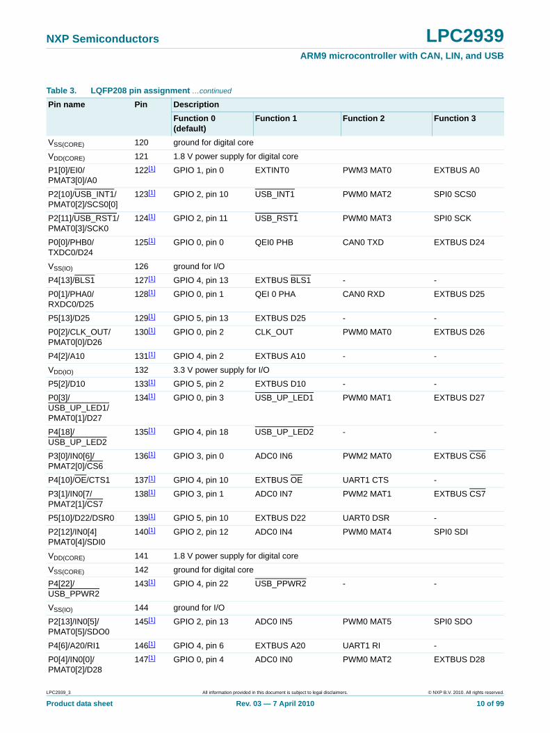
Pin name Pin Description
Function 0 (default)
Function 1 Function 2 Function 3
LPC2939_3 All information provided in this document is subject to legal disclaimers. © NXP B.V. 2010. All rights reserved.
Product data sheet Rev. 03 — 7 April 2010 10 of 99
NXP Semiconductors LPC2939ARM9 microcontroller with CAN, LIN, and USB
P5[6]/D18/RI0 148[1] GPIO 5, pin 6 EXTBUS D18 UART0 RI -
P4[14]/BLS2 149[1] GPIO 4, pin 14 EXTBUS BLS2 - -
P0[5]/IN0[1]/PMAT0[3]/D29
150[1] GPIO 0, pin 5 ADC0 IN1 PWM0 MAT3 EXTBUS D29
P5[14]/USB_SSPND1/RTS0
151[1] GPIO 5, pin 14 USB_SSPND1 UART0 RTS -
VDD(IO) 152 3.3 V power supply for I/O
P0[6]/IN0[2]/PMAT0[4]/D30
153[1] GPIO 0, pin 6 ADC0 IN2 PWM0 MAT4 EXTBUS D30
P0[7]/IN0[3]/PMAT0[5]/D31
154[1] GPIO 0, pin 7 ADC0 IN3 PWM0 MAT5 EXTBUS D31
VDDA(ADC3V3) 155 3.3 V power supply for ADC
JTAGSEL 156[1] TAP controller select input; LOW-level selects the ARM debug mode; HIGH-level selects boundary scan; pulled up internally
VDDA(ADC5V0) 157 5 V supply voltage for ADC0 and 5 V reference for ADC0
VREFP 158[3] HIGH reference for ADC
VREFN 159[3] LOW reference for ADC
P0[8]/IN1[0]/TXDL0/A20
160[4] GPIO 0, pin 8 ADC1 IN0 LIN0 TXD/ UART TXD EXTBUS A20
P0[9]/IN1[1]/RXDL0/A21
161[4] GPIO 0, pin 9 ADC1 IN1 LIN0 RXD/ UART TXD EXTBUS A21
P0[10]/IN1[2]/PMAT1[0]/A8
162[4] GPIO 0, pin 10 ADC1 IN2 PWM1 MAT0 EXTBUS A8
P0[11]/IN1[3]/PMAT1[1]/A9
163[4] GPIO 0, pin 11 ADC1 IN3 PWM1 MAT1 EXTBUS A9
P2[14]/SDA1/PCAP0[0]/BLS0
164[1] GPIO 2, pin 14 I2C1 SDA PWM0 CAP0 EXTBUS BLS0
P2[15]/SCL1/PCAP0[1]/BLS1
165[1] GPIO 2, pin 15 I2C1 SCL PWM0 CAP1 EXTBUS BLS1
P3[2]/MAT3[0]/PMAT2[2]/USB_SDA1
166[1] GPIO 3, pin 2 TIMER3 MAT0 PWM2 MAT2 USB_SDA1
VDD(CORE) 167 1.8 V power supply for digital core
VSS(CORE) 168 ground for digital core
VSS(IO) 169 ground for I/O
P4[3]/A11 170[1] GPIO 4, pin 3 EXTBUS A11 - -
P3[3]/MAT3[1]/PMAT2[3]/USB_SCL1
171[1] GPIO 3, pin 3 TIMER3 MAT1 PWM2 MAT3 USB_SCL1
P5[3]/D11 172[1] GPIO 5, pin 3 EXTBUS D11 - -
P0[12]/IN1[4]/PMAT1[2]/A10
173[4] GPIO 0, pin 12 ADC1 IN4 PWM1 MAT2 EXTBUS A10
P4[19]/USB_CONNECT2
174[1] GPIO 4, pin 19 USB_CONNECT2 - -
Table 3. LQFP208 pin assignment …continued
Pin name Pin Description
Function 0 (default)
Function 1 Function 2 Function 3
LPC2939_3 All information provided in this document is subject to legal disclaimers. © NXP B.V. 2010. All rights reserved.
Product data sheet Rev. 03 — 7 April 2010 11 of 99
NXP Semiconductors LPC2939ARM9 microcontroller with CAN, LIN, and USB
P0[13]/IN1[5]/PMAT1[3]/A11
175[4] GPIO 0, pin 13 ADC1 IN5 PWM1 MAT3 EXTBUS A11
VDD(IO) 176 3.3 V power supply for I/O
P4[11]/WE/CTS0 177[1] GPIO 4, pin 11 EXTBUS WE UART0 CTS -
P0[14]/IN1[6]/PMAT1[4]/A12
178[4] GPIO 0, pin 14 ADC1 IN6 PWM1 MAT4 EXTBUS A12
P5[11]/D23/DCD0 179[1] GPIO 5, pin 11 EXTBUS D23 UART0 DCD -
P0[15]/IN1[7]/PMAT1[5]/A13
180[4] GPIO 0, pin 15 ADC1 IN7 PWM1 MAT5 EXTBUS A13
P4[23]/USB_PWRD2
181[1] GPIO 4, pin 23 USB_PWRD2 - -
P0[16]IN2[0]/TXD0/A22
182[4] GPIO 0, pin 16 ADC2 IN0 UART0 TXD EXTBUS A22
P4[7]/A21/DTR1 183[1] GPIO 4, pin 7 EXTBUS A21 UART1 DTR -
VSS(IO) 184 ground for I/O
P5[7]/D19/U0OUT1
185[1] GPIO 5, pin 7 EXTBUS D19 UART0 OUT1 -
P0[17]/IN2[1]/RXD0/A23
186[4] GPIO 0, pin 17 ADC2 IN1 UART0 RXD EXTBUS A23
P4[15]/BLS3 187[1] GPIO 4, pin 15 EXTBUS BLS3 - -
P5[15]/USB_UP_LED1/RTS1
188[1] GPIO 5, pin 15 USB_UP_LED1 UART1 RTS -
VDD(CORE) 189 1.8 V power supply for digital core
VSS(CORE) 190 ground for digital core
P2[16]/TXD1/PCAP0[2]/BLS2
191[1] GPIO 2, pin 16 UART1 TXD PWM0 CAP2 EXTBUS BLS2
P2[17]/RXD1/PCAP1[0]/BLS3
192[1] GPIO 2, pin 17 UART1 RXD PWM1 CAP0 EXTBUS BLS3
VDD(IO) 193 3.3 V power supply for I/O
P0[18]/IN2[2]/PMAT2[0]/A14
194[4] GPIO 0, pin 18 ADC2 IN2 PWM2 MAT0 EXTBUS A14
P0[19]/IN2[3]/PMAT2[1]/A15
195[4] GPIO 0, pin 19 ADC2 IN3 PWM2 MAT1 EXTBUS A15
P3[4]/MAT3[2]/PMAT2[4]/TXDC1
196[1] GPIO 3, pin 4 TIMER3 MAT2 PWM2 MAT4 CAN1 TXD
P3[5]/MAT3[3]/PMAT2[5]/RXDC1
197[1] GPIO 3, pin 5 TIMER3 MAT3 PWM2 MAT5 CAN1 RXD
P2[18]/SCS2[1]/PCAP1[1]/D16
198[1] GPIO 2, pin 18 SPI2 SCS1 PWM1 CAP1 EXTBUS D16
P2[19]/SCS2[0]/PCAP1[2]/D17
199[1] GPIO 2, pin 19 SPI2 SCS0 PWM1 CAP2 EXTBUS D17
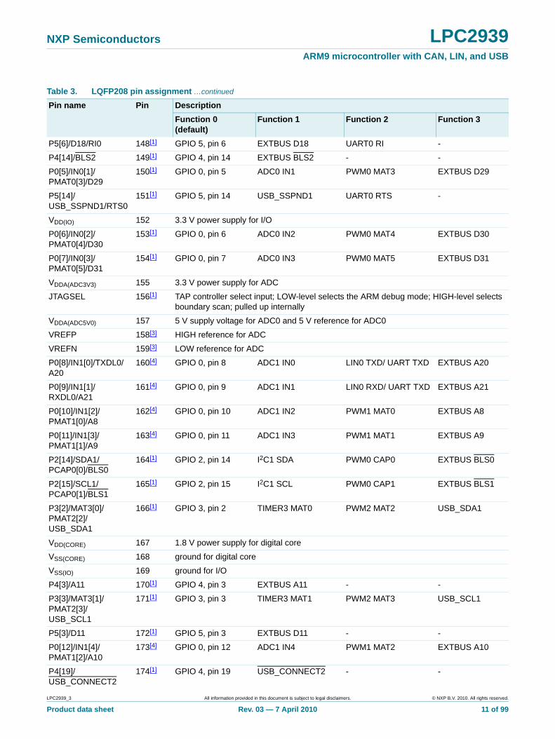
Table 3. LQFP208 pin assignment …continued
Pin name Pin Description
Function 0 (default)
Function 1 Function 2 Function 3
LPC2939_3 All information provided in this document is subject to legal disclaimers. © NXP B.V. 2010. All rights reserved.
Product data sheet Rev. 03 — 7 April 2010 12 of 99
NXP Semiconductors LPC2939ARM9 microcontroller with CAN, LIN, and USB
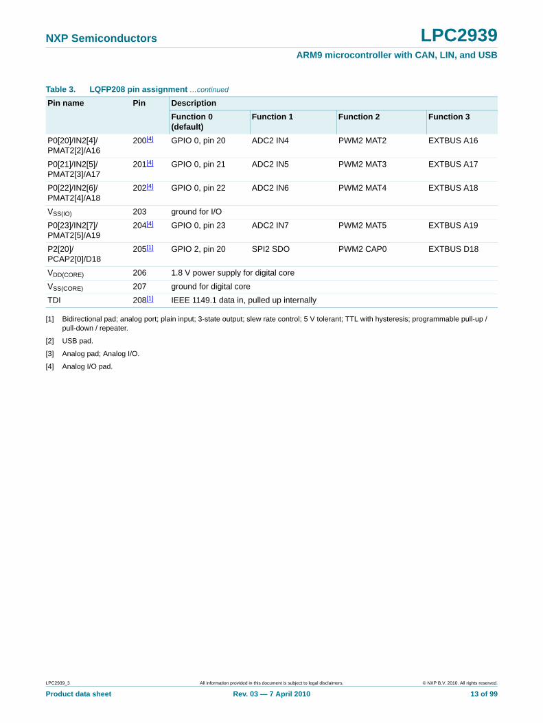
[1] Bidirectional pad; analog port; plain input; 3-state output; slew rate control; 5 V tolerant; TTL with hysteresis; programmable pull-up / pull-down / repeater.
[2] USB pad.
[3] Analog pad; Analog I/O.
[4] Analog I/O pad.
P0[20]/IN2[4]/PMAT2[2]/A16
200[4] GPIO 0, pin 20 ADC2 IN4 PWM2 MAT2 EXTBUS A16
P0[21]/IN2[5]/PMAT2[3]/A17
201[4] GPIO 0, pin 21 ADC2 IN5 PWM2 MAT3 EXTBUS A17
P0[22]/IN2[6]/PMAT2[4]/A18
202[4] GPIO 0, pin 22 ADC2 IN6 PWM2 MAT4 EXTBUS A18
VSS(IO) 203 ground for I/O
P0[23]/IN2[7]/PMAT2[5]/A19
204[4] GPIO 0, pin 23 ADC2 IN7 PWM2 MAT5 EXTBUS A19
P2[20]/PCAP2[0]/D18
205[1] GPIO 2, pin 20 SPI2 SDO PWM2 CAP0 EXTBUS D18
VDD(CORE) 206 1.8 V power supply for digital core
VSS(CORE) 207 ground for digital core
TDI 208[1] IEEE 1149.1 data in, pulled up internally
Table 3. LQFP208 pin assignment …continued
Pin name Pin Description
Function 0 (default)
Function 1 Function 2 Function 3
LPC2939_3 All information provided in this document is subject to legal disclaimers. © NXP B.V. 2010. All rights reserved.
Product data sheet Rev. 03 — 7 April 2010 13 of 99
NXP Semiconductors LPC2939ARM9 microcontroller with CAN, LIN, and USB
6. Functional description
6.1 Architectural overview
The LPC2939 consists of:
• An ARM968E-S processor with real-time emulation support
• An AMBA multilayer Advanced High-performance Bus (AHB) for interfacing to the on-chip memory controllers
• Two DTL buses (an universal NXP interface) for interfacing to the interrupt controller and the Power, Clock and Reset Control SubSystem (PCRSS)
• Three ARM Peripheral Buses (APB - a compatible super set of ARM's AMBA advanced peripheral bus) for connection to on-chip peripherals clustered in subsystems
• One ARM Peripheral Bus for event router and system control
The LPC2939 configures the ARM968E-S processor in little-endian byte order. All peripherals run at their own clock frequency to optimize the total system power consumption. The AHB-to-APB bridge used in the subsystems contains a write-ahead buffer one transaction deep. This implies that when the ARM968E-S issues a buffered write action to a register located on the APB side of the bridge, it continues even though the actual write may not yet have taken place. Completion of a second write to the same subsystem will not be executed until the first write is finished.
6.2 ARM968E-S processor
The ARM968E-S is a general purpose 32-bit RISC processor, which offers high performance and very low power consumption. The ARM architecture is based on Reduced Instruction Set Computer (RISC) principles, and the instruction set and related decode mechanism are much simpler than those of microprogrammed Complex Instruction Set Computers (CISC). This simplicity results in a high instruction throughput and impressive real-time interrupt response from a small and cost-effective controller core.
Amongst the most compelling features of the ARM968E-S are:
• Separate directly connected instruction and data Tightly Coupled Memory (TCM) interfaces
• Write buffers for the AHB and TCM buses
• Enhanced 16 32 multiplier capable of single-cycle MAC operations and 16-bit fixed- point DSP instructions to accelerate signal-processing algorithms and applications
Pipeline techniques are employed so that all parts of the processing and memory systems can operate continuously. The ARM968E-S is based on the ARMv5TE five-stage pipeline architecture. Typically, in a three-stage pipeline architecture, while one instruction is being executed its successor is being decoded and a third instruction is being fetched from memory. In the five-stage pipeline additional stages are added for memory access and write-back cycles.
LPC2939_3 All information provided in this document is subject to legal disclaimers. © NXP B.V. 2010. All rights reserved.
Product data sheet Rev. 03 — 7 April 2010 14 of 99
NXP Semiconductors LPC2939ARM9 microcontroller with CAN, LIN, and USB
The ARM968E-S processor also employs a unique architectural strategy known as THUMB, which makes it ideally suited to high-volume applications with memory restrictions or to applications where code density is an issue.
The key idea behind THUMB is that of a super-reduced instruction set. Essentially, the ARM968E-S processor has two instruction sets:
• Standard 32-bit ARMv5TE set
• 16-bit THUMB set
The THUMB set's 16-bit instruction length allows it to approach twice the density of standard ARM code while retaining most of the ARM's performance advantage over a traditional 16-bit controller using 16-bit registers. This is possible because THUMB code operates on the same 32-bit register set as ARM code.
THUMB code can provide up to 65 % of the code size of ARM, and 160 % of the performance of an equivalent ARM controller connected to a 16-bit memory system.
The ARM968E-S processor is described in detail in the ARM968E-S data sheet Ref. 2.
6.3 On-chip flash memory system
The LPC2939 includes a 768 kB flash memory system. This memory can be used for both code and data storage. Programming of the flash memory can be accomplished via the flash memory controller or the JTAG.
The flash controller also supports a 16 kB, byte-accessible on-chip EEPROM integrated on the LPC2939.
6.4 On-chip static RAM
In addition to the two 32 kB TCMs the LPC2939 includes two static RAM memories: one of 32 kB and one of 16 kB. Both may be used for code and/or data storage.
In addition, 8 kB SRAM for the ETB can be used as static memory for code and data storage. However, DMA access to this memory region is not supported.
LPC2939_3 All information provided in this document is subject to legal disclaimers. © NXP B.V. 2010. All rights reserved.
Product data sheet Rev. 03 — 7 April 2010 15 of 99
xxxxxxxxxxxxxxxxxxxxx xxxxxxxxxxxxxxxxxxxxxxxxxx xxxxxxx x x x xxxxxxxxxxxxxxxxxxxxxxxxxxxxxx xxxxxxxxxxxxxxxxxxx xx xx xxxxx xxxxxxxxxxxxxxxxxxxxxxxxxxx xxxxxxxxxxxxxxxxxxx xxxxxx xxxxxxxxxxxxxxxxxxxxxxxxxxxxxxxxxxx xxxxxxxxxxxx x x xxxxxxxxxxxxxxxxxxxxx xxxxxxxxxxxxxxxxxxxxxxxxxxxxxx xxxxx xxxxxxxxxxxxxxxxxxxxxxxxxxxxxxxxxxxxxxxxxxxxxxxxxx xxxxxxxx xxxxxxxxxxxxxxxxxxxxxxxxx xxxxxxxxxxxxxxxxxxxx xxx
LPC
2939_3
Pro
du
ct data sh
eetR
ev. 03 —
7 Ap
ril 2010 16 o
f 99
NX
P S
emico
nd
ucto
rsL
PC
2939A
RM
9 m
icro
co
ntro
ller w
ith C
AN
, LIN
, and
US
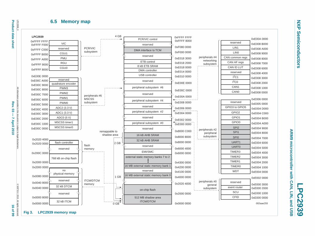
B6.5 Memory map
0xE004 1000
0xE004 2000
0xE004 3000
0xE004 4000
0xE004 6000
0xE004 8000
0xE004 A000
0xE004 B000
0xE004 D000
0xE005 0000
0xE006 0000
0xE004 C000
0xE004 9000
0xE004 7000
0xE004 5000
0xE004 0000
SPI0
WDT
TIMER0
TIMER1
TIMER2
TIMER3
UART0
UART1
SPI1
SPI2
GPIO0
GPIO1
GPIO2
GPIO3 to GPIO5
0xE000 1000
0xE000 20000xE000 3000
0xE002 0000
0xE000 0000CFID
SCU
event router
0xE008 1000
0xE008 0000CAN0
CAN10xE008 2000
0xE008 3000
0xE008 4000
0xE008 7000
0xE008 9000
0xE008 B000
0xE00A 0000
0xE008 A000
0xE008 8000
0xE008 6000
I2C0
I2C1
reserved
CAN ID LUT
CAN common regs
LIN0
LIN1
CAN AF regs
reserved
reserved
reserved
002aae255
All inform
ation provided
in this docum
ent is subject to leg
al disclaim
ers.©
NX
P B
.V. 2010. A
ll rights reserved.
Fig 3. LPC2939 memory map
16 MB external static memory bank 0
16 MB external static memory bank 1
external static memory banks 7 to 2
reserved
DMA interface to TCM
PCR/VIC control
0x0000 00000 GB
1 GB
4 GB
2 GB
0x4000 0000
0x4100 0000
0x4300 0000
0x4200 0000
0x2000 0000
0x6000 0000
0x6000 4000
0x8000 0000
0x8000 8000
0x8000 C000
0xE000 0000
0xE002 0000
0xE004 0000
0xE006 0000
0xE008 0000
0xE00A 0000
0xE00C 0000
0xE00E 0000
0xE010 0000
0xE014 0000
0xE018 3000
0xF000 0000
0xF080 0000
0xFFFF 80000xFFFF FFFF
reserved
reserved
reserved
reserved
reserved
reserved
peripheral subsystem #0
peripheral subsystem #2
peripheral subsystem #4
peripheral subsystem #6
0xE018 2000
0xE018 0000
32 kB AHB SRAM
16 kB AHB SRAM
reserved
USB controller
DMA controller
8 kB ETB SRAM
ETB control
reserved
ITCM/DTCM
on-chip flash
0x2020 4000
0x0000 0000
0x0040 0000
0x0000 8000
0x0040 8000
0x0080 0000
0x2000 0000
32 kB ITCM
32 kB DTCM
reserved
reserved
nophysical memory
peripherals #6MSCSSsubsystem
ITCM/DTCMmemory
EMI/SMC
peripherals #2peripheral
subsystem
peripherals #0general
subsystem
peripherals #4networkingsubsystem
0xE00C 0000
0xE00C 1000
0xE00C 2000
0xE00C 3000
0xE00C 4000
0xE00C 5000
0xE00C 6000
0xE00C 7000
0xE00C 8000
0xE00C 9000
0xE00C A000
0xE00E 0000
ADC0 (5 V)
ADC1 (3.3 V)
ADC2 (3.3 V)
PWM0
PWM1
PWM3
quadrature encoder
PWM2
MSCSS timer0
MSCSS timer1
PCR/VICsubsystem
0xFFFF 8000
0xFFFF 9000
0xFFFF A000
0xFFFF B000
0xFFFF C000
0xFFFF F0000xFFFF FFFF
PMU
CGU1
reserved
reserved
VIC
CGU0
RGU
512 MB shadow area
remappable to shadow area
LPC2939
768 kB on-chip flash
flash controller
0x2000 0000
reserved
0x200C 0000
0x2020 0000
0x2020 4000
flashmemory
NXP Semiconductors LPC2939ARM9 microcontroller with CAN, LIN, and USB
6.6 Reset, debug, test, and power description
6.6.1 Reset and power-up behavior
The LPC2939 contains external reset input and internal power-up reset circuits. This ensures that a reset is extended internally until the oscillators and flash have reached a stable state. See Section 8 for trip levels of the internal power-up reset circuit1. See Section 9 for characteristics of the several start-up and initialization times. Table 4 shows the reset pin.
At activation of the RST pin the JTAGSEL pin is sensed as logic LOW. If this is the case the LPC2939 is assumed to be connected to debug hardware, and internal circuits re-program the source for the BASE_SYS_CLK to be the crystal oscillator instead of the Low-Power Ring Oscillator (LP_OSC). This is required because the clock rate when running at LP_OSC speed is too low for the external debugging environment.
6.6.2 Reset strategy
The LPC2939 contains a central module, the Reset Generator Unit (RGU) in the Power, Clock and Reset Subsystem (PCRSS), which controls all internal reset signals towards the peripheral modules. The RGU provides individual reset control as well as the monitoring functions needed for tracing a reset back to source.
6.6.3 IEEE 1149.1 interface pins (JTAG boundary-scan test)
The LPC2939 contains boundary-scan test logic according to IEEE 1149.1, also referred to in this document as Joint Test Action Group (JTAG). The boundary-scan test pins can be used to connect a debugger probe for the embedded ARM processor. Pin JTAGSEL selects between boundary-scan mode and debug mode. Table 5 shows the boundary- scan test pins.
1. Only for 1.8 V power sources
Table 4. Reset pin
Symbol Direction Description
RST IN external reset input, active LOW; pulled up internally
Table 5. IEEE 1149.1 boundary-scan test and debug interface
Symbol Description
JTAGSEL TAP controller select input. LOW level selects ARM debug mode and HIGH level selects boundary scan and flash programming; pulled up internally
TRST test reset input; pulled up internally (active LOW)
TMS test mode select input; pulled up internally
TDI test data input, pulled up internally
TDO test data output
TCK test clock input
LPC2939_3 All information provided in this document is subject to legal disclaimers. © NXP B.V. 2010. All rights reserved.
Product data sheet Rev. 03 — 7 April 2010 17 of 99
NXP Semiconductors LPC2939ARM9 microcontroller with CAN, LIN, and USB
6.6.3.1 ETM/ETB
The ETM provides real-time trace capability for deeply embedded processor cores. It outputs information about processor execution to a trace buffer. A software debugger allows configuration of the ETM using a JTAG interface and displays the trace information that has been captured in a format that a user can easily understand. The ETB stores trace data produced by the ETM.
The ETM/ETB module has the following features:
• Closely tracks the instructions that the ARM core is executing
• On-chip trace data storage (ETB)
• All registers are programmed through JTAG interface
• Does not consume power when trace is not being used
• THUMB/Java instruction set support
6.6.4 Power supply pins
Table 6 shows the power supply pins.
6.7 Clocking strategy
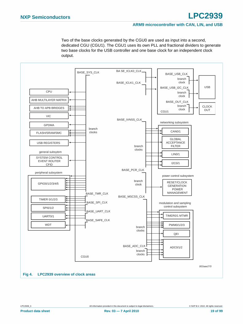
6.7.1 Clock architecture
The LPC2939 contains several different internal clock areas. Peripherals like Timers, SPI, UART, CAN and LIN have their own individual clock sources called base clocks. All base clocks are generated by the Clock Generator Unit (CGU0). They may be unrelated in frequency and phase and can have different clock sources within the CGU.
The system clock for the CPU and AHB Bus infrastructure has its own base clock. This means most peripherals are clocked independently from the system clock. See Figure 4 for an overview of the clock areas within the device.
Within each clock area there may be multiple branch clocks, which offers very flexible control for power-management purposes. All branch clocks are outputs of the Power Management Unit (PMU) and can be controlled independently. Branch clocks derived from the same base clock are synchronous in frequency and phase. See Section 6.16 for more details of clock and power control within the device.
Table 6. Power supply pins
Symbol Description
VDD(CORE) digital core supply 1.8 V
VSS(CORE) digital core ground (digital core, ADC0/1/2)
VDD(IO) I/O pins supply 3.3 V
VSS(IO) I/O pins ground
VDD(OSC_PLL) oscillator and PLL supply
VSS(OSC) oscillator ground
VSS(PLL) PLL ground
VDDA(ADC3V3) ADC1 and ADC2 3.3 V supply
VDDA(ADC5V0) ADC0 5.0 V supply
LPC2939_3 All information provided in this document is subject to legal disclaimers. © NXP B.V. 2010. All rights reserved.
Product data sheet Rev. 03 — 7 April 2010 18 of 99
NXP Semiconductors LPC2939ARM9 microcontroller with CAN, LIN, and USB
Two of the base clocks generated by the CGU0 are used as input into a second, dedicated CGU (CGU1). The CGU1 uses its own PLL and fractional dividers to generate two base clocks for the USB controller and one base clock for an independent clock output.
Fig 4. LPC2939 overview of clock areas
TIMER0/1 MTMR
PWM0/1/2/3
ADC0/1/2
QEI
modulation and sampling control subsystem
BASE_MSCSS_CLK
branchclocks
branchclocks
BASE_ADC_CLK
BA SE_ICLK0_CLK
BASE_ICLK1_CLK
CAN0/1
GLOBALACCEPTANCE
FILTER
LIN0/1
I2C0/1
networking subsystemBASE_IVNSS_CLK
branchclocks
RESET/CLOCK GENERATION
POWERMANAGEMENT
power control subsystem
BASE_PCR_CLK
branchclockGPIO0/1/2/3/4/5
TIMER 0/1/2/3
SPI0/1/2
UART0/1
WDT
BASE_SYS_CLK
CPU
AHB MULTILAYER MATRIX
VIC
GPDMA
USB REGISTERS
FLASH/SRAM/SMC
general subsytem
peripheral subsystem
AHB TO APB BRIDGES
SYSTEM CONTROLEVENT ROUTER
CFID
branchclocks
branchclock
branchclock
branchclock
BASE_SAFE_CLK
BASE_UART_CLK
BASE_SPI_CLK
BASE_TMR_CLK
002aae270
CGU0
CGU1
BASE_USB_CLK
BASE_USB_I2C_CLK
BASE_OUT_CLK
USB
CLOCKOUT
LPC2939_3 All information provided in this document is subject to legal disclaimers. © NXP B.V. 2010. All rights reserved.
Product data sheet Rev. 03 — 7 April 2010 19 of 99
NXP Semiconductors LPC2939ARM9 microcontroller with CAN, LIN, and USB
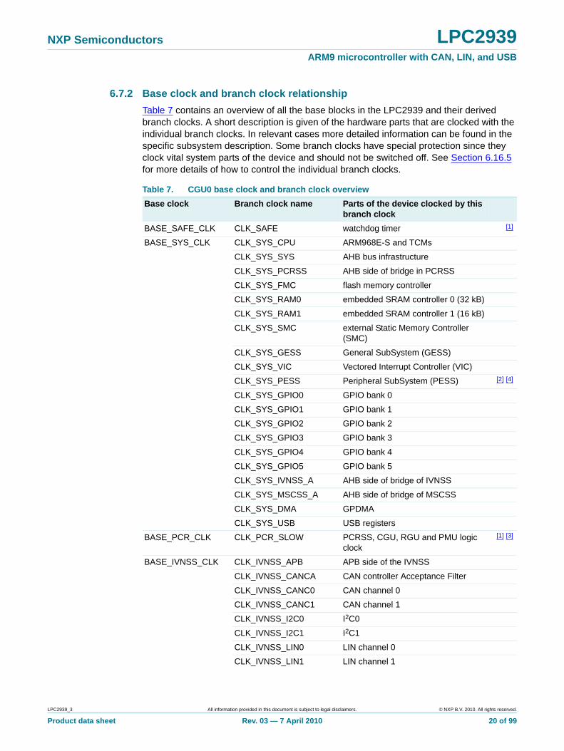
6.7.2 Base clock and branch clock relationship
Table 7 contains an overview of all the base blocks in the LPC2939 and their derived branch clocks. A short description is given of the hardware parts that are clocked with the individual branch clocks. In relevant cases more detailed information can be found in the specific subsystem description. Some branch clocks have special protection since they clock vital system parts of the device and should not be switched off. See Section 6.16.5 for more details of how to control the individual branch clocks.
Table 7. CGU0 base clock and branch clock overview
Base clock Branch clock name Parts of the device clocked by this branch clock
BASE_SAFE_CLK CLK_SAFE watchdog timer [1]
BASE_SYS_CLK CLK_SYS_CPU ARM968E-S and TCMs
CLK_SYS_SYS AHB bus infrastructure
CLK_SYS_PCRSS AHB side of bridge in PCRSS
CLK_SYS_FMC flash memory controller
CLK_SYS_RAM0 embedded SRAM controller 0 (32 kB)
CLK_SYS_RAM1 embedded SRAM controller 1 (16 kB)
CLK_SYS_SMC external Static Memory Controller (SMC)
CLK_SYS_GESS General SubSystem (GESS)
CLK_SYS_VIC Vectored Interrupt Controller (VIC)
CLK_SYS_PESS Peripheral SubSystem (PESS) [2] [4]
CLK_SYS_GPIO0 GPIO bank 0
CLK_SYS_GPIO1 GPIO bank 1
CLK_SYS_GPIO2 GPIO bank 2
CLK_SYS_GPIO3 GPIO bank 3
CLK_SYS_GPIO4 GPIO bank 4
CLK_SYS_GPIO5 GPIO bank 5
CLK_SYS_IVNSS_A AHB side of bridge of IVNSS
CLK_SYS_MSCSS_A AHB side of bridge of MSCSS
CLK_SYS_DMA GPDMA
CLK_SYS_USB USB registers
BASE_PCR_CLK CLK_PCR_SLOW PCRSS, CGU, RGU and PMU logic clock
[1] [3]
BASE_IVNSS_CLK CLK_IVNSS_APB APB side of the IVNSS
CLK_IVNSS_CANCA CAN controller Acceptance Filter
CLK_IVNSS_CANC0 CAN channel 0
CLK_IVNSS_CANC1 CAN channel 1
CLK_IVNSS_I2C0 I2C0
CLK_IVNSS_I2C1 I2C1
CLK_IVNSS_LIN0 LIN channel 0
CLK_IVNSS_LIN1 LIN channel 1
LPC2939_3 All information provided in this document is subject to legal disclaimers. © NXP B.V. 2010. All rights reserved.
Product data sheet Rev. 03 — 7 April 2010 20 of 99
NXP Semiconductors LPC2939ARM9 microcontroller with CAN, LIN, and USB
[1] This clock is always on (cannot be switched off for system safety reasons).
[2] In the peripheral subsystem parts of the Timers, watchdog timer, SPI and UART have their own clock source. See Section 6.13 for details.
[3] In the Power Clock and Reset Control subsystem parts of the CGU, RGU, and PMU have their own clock source. See Section 6.16 for details.
[4] The clock should remain activated when system wake-up on timer or UART is required.
BASE_MSCSS_CLK CLK_MSCSS_APB APB side of the MSCSS
CLK_MSCSS_MTMR0 timer 0 in the MSCSS
CLK_MSCSS_MTMR1 timer 1 in the MSCSS
CLK_MSCSS_PWM0 PWM 0
CLK_MSCSS_PWM1 PWM 1
CLK_MSCSS_PWM2 PWM 2
CLK_MSCSS_PWM3 PWM 3
CLK_MSCSS_ADC0_APB APB side of ADC 0
CLK_MSCSS_ADC1_APB APB side of ADC 1
CLK_MSCSS_ADC2_APB APB side of ADC 2
CLK_MSCSS_QEI Quadrature Encoder Interface (QEI)
BASE_UART_CLK CLK_UART0 UART 0 interface clock
CLK_UART1 UART 1 interface clock
BASE_ICLK0_CLK - CGU1 input clock
BASE_SPI_CLK CLK_SPI0 SPI 0 interface clock
CLK_SPI1 SPI 1 interface clock
CLK_SPI2 SPI 2 interface clock
BASE_TMR_CLK CLK_TMR0 timer 0 clock for counter part
CLK_TMR1 timer 1 clock for counter part
CLK_TMR2 timer 2 clock for counter part
CLK_TMR3 timer 3 clock for counter part
BASE_ADC_CLK CLK_ADC0 control of ADC 0, capture sample result
CLK_ADC1 control of ADC 1, capture sample result
CLK_ADC2 control of ADC 2, capture sample result
- reserved -
BASE_ICLK1_CLK - CGU1 input clock
Table 8. CGU1 base clock and branch clock overview
Base clock Branch clock name Parts of the device clocked by this branch clock
BASE_OUT_CLK CLK_OUT_CLK pin CLK_OUT
BASE_USB_CLK CLK_USB_CLK USB clock
BASE_USB_I2C_CLK CLK_USB_I2C_CLK USB OTG I2C clock
Table 7. CGU0 base clock and branch clock overview …continued
Base clock Branch clock name Parts of the device clocked by this branch clock
LPC2939_3 All information provided in this document is subject to legal disclaimers. © NXP B.V. 2010. All rights reserved.
Product data sheet Rev. 03 — 7 April 2010 21 of 99
NXP Semiconductors LPC2939ARM9 microcontroller with CAN, LIN, and USB
6.8 Flash memory controller
The flash memory has a 128-bit wide data interface and the flash controller offers two 128-bit buffer lines to improve system performance. The flash has to be programmed initially via JTAG. In-system programming must be supported by the bootloader. Flash memory contents can be protected by disabling JTAG access. Suspension of burning or erasing is not supported.
The Flash Memory Controller (FMC) interfaces to the embedded flash memory for two tasks:
• Memory data transfer
• Memory configuration via triggering, programming, and erasing
The key features are:
• Programming by CPU via AHB
• Programming by external programmer via JTAG
• JTAG access protection
• Burn-finished and erase-finished interrupt
6.8.1 Functional description
After reset flash initialization is started. During this initialization, flash access is not possible and AHB transfers to flash are stalled, blocking the AHB bus.
During flash initialization, the index sector is read to identify the status of the JTAG access protection and sector security. If JTAG access protection is active, the flash is not accessible via JTAG. In this case, ARM debug facilities are disabled and flash-memory contents cannot be read. If sector security is active, only the unsecured sections can be read.
Flash can be read synchronously or asynchronously to the system clock. In synchronous operation, the flash goes into standby after returning the read data. Started reads cannot be stopped, and speculative reading and dual buffering are therefore not supported.
With asynchronous reading, transfer of the address to the flash and of read data from the flash is done asynchronously, giving the fastest possible response time. Started reads can be stopped, so speculative reading and dual buffering are supported.
Buffering is offered because the flash has a 128-bit wide data interface while the AHB interface has only 32 bits. With buffering a buffer line holds the complete 128-bit flash word, from which four words can be read. Without buffering every AHB data port read starts a flash read. A flash read is a slow process compared to the minimum AHB cycle time, so with buffering the average read time is reduced improving system performance.
With single buffering, the most recently read flash word remains available until the next flash read. When an AHB data-port read transfer requires data from the same flash word as the previous read transfer, no new flash read is done and the read data is given without wait cycles.
When an AHB data port read transfer requires data from a different flash word to that involved in the previous read transfer, a new flash read is done and wait states are given until the new read data is available.
LPC2939_3 All information provided in this document is subject to legal disclaimers. © NXP B.V. 2010. All rights reserved.
Product data sheet Rev. 03 — 7 April 2010 22 of 99
NXP Semiconductors LPC2939ARM9 microcontroller with CAN, LIN, and USB
With dual buffering, a secondary buffer line is used, the output of the flash being considered as the primary buffer. On a primary buffer, hit data can be copied to the secondary buffer line, which allows the flash to start a speculative read of the next flash word.
Both buffer lines are invalidated after:
• Initialization
• Configuration-register access
• Data-latch reading
• Index-sector reading
The modes of operation are listed in Table 9.
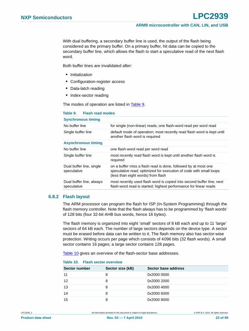
6.8.2 Flash layout
The ARM processor can program the flash for ISP (In-System Programming) through the flash memory controller. Note that the flash always has to be programmed by ‘flash words’ of 128 bits (four 32-bit AHB bus words, hence 16 bytes).
The flash memory is organized into eight ‘small’ sectors of 8 kB each and up to 11 ‘large’ sectors of 64 kB each. The number of large sectors depends on the device type. A sector must be erased before data can be written to it. The flash memory also has sector-wise protection. Writing occurs per page which consists of 4096 bits (32 flash words). A small sector contains 16 pages; a large sector contains 128 pages.
Table 10 gives an overview of the flash-sector base addresses.
Table 9. Flash read modes
Synchronous timing
No buffer line for single (non-linear) reads; one flash-word read per word read
Single buffer line default mode of operation; most recently read flash word is kept until another flash word is required
Asynchronous timing
No buffer line one flash-word read per word read
Single buffer line most recently read flash word is kept until another flash word is required
Dual buffer line, single speculative
on a buffer miss a flash read is done, followed by at most one speculative read; optimized for execution of code with small loops (less than eight words) from flash
Dual buffer line, always speculative
most recently used flash word is copied into second buffer line; next flash-word read is started; highest performance for linear reads
Table 10. Flash sector overview
Sector number Sector size (kB) Sector base address
11 8 0x2000 0000
12 8 0x2000 2000
13 8 0x2000 4000
14 8 0x2000 6000
15 8 0x2000 8000
LPC2939_3 All information provided in this document is subject to legal disclaimers. © NXP B.V. 2010. All rights reserved.
Product data sheet Rev. 03 — 7 April 2010 23 of 99
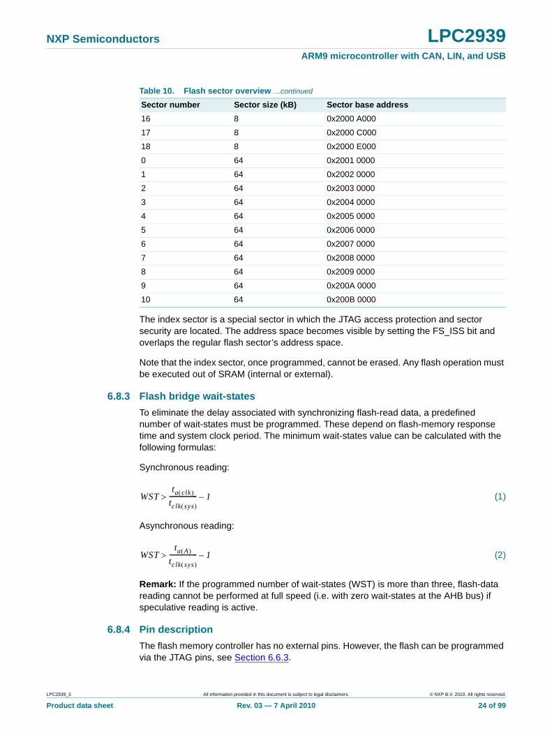
NXP Semiconductors LPC2939ARM9 microcontroller with CAN, LIN, and USB
The index sector is a special sector in which the JTAG access protection and sector security are located. The address space becomes visible by setting the FS_ISS bit and overlaps the regular flash sector’s address space.
Note that the index sector, once programmed, cannot be erased. Any flash operation must be executed out of SRAM (internal or external).
6.8.3 Flash bridge wait-states
To eliminate the delay associated with synchronizing flash-read data, a predefined number of wait-states must be programmed. These depend on flash-memory response time and system clock period. The minimum wait-states value can be calculated with the following formulas:
Synchronous reading:
(1)
Asynchronous reading:
(2)
Remark: If the programmed number of wait-states (WST) is more than three, flash-data reading cannot be performed at full speed (i.e. with zero wait-states at the AHB bus) if speculative reading is active.
6.8.4 Pin description
The flash memory controller has no external pins. However, the flash can be programmed via the JTAG pins, see Section 6.6.3.
16 8 0x2000 A000
17 8 0x2000 C000
18 8 0x2000 E000
0 64 0x2001 0000
1 64 0x2002 0000
2 64 0x2003 0000
3 64 0x2004 0000
4 64 0x2005 0000
5 64 0x2006 0000
6 64 0x2007 0000
7 64 0x2008 0000
8 64 0x2009 0000
9 64 0x200A 0000
10 64 0x200B 0000
Table 10. Flash sector overview …continued
Sector number Sector size (kB) Sector base address
WSTta clk
tclk sys ------------------ 1–
WSTta A
tclk sys ------------------ 1–
LPC2939_3 All information provided in this document is subject to legal disclaimers. © NXP B.V. 2010. All rights reserved.
Product data sheet Rev. 03 — 7 April 2010 24 of 99
NXP Semiconductors LPC2939ARM9 microcontroller with CAN, LIN, and USB
6.8.5 Clock description
The flash memory controller is clocked by CLK_SYS_FMC, see Section 6.7.2.
6.8.6 EEPROM
EEPROM is a non-volatile memory mostly used for storing relatively small amounts of data, for example for storing settings. It contains one 16 kB memory block and is byte-programmable and byte-erasable.
The EEPROM can be accessed only through the flash controller.
6.9 External Static Memory Controller (SMC)
The LPC2939 contains an external Static Memory Controller (SMC) which provides an interface for external (off-chip) memory devices.
Key features are:
• Supports static memory-mapped devices including RAM, ROM, flash, burst ROM and external I/O devices
• Asynchronous page-mode read operation in non-clocked memory subsystems
• Asynchronous burst-mode read access to burst-mode ROM devices
• Independent configuration for up to eight banks, each up to 16 MB
• Programmable bus-turnaround (idle) cycles (one to 16)
• Programmable read and write wait states (up to 32), for static RAM devices
• Programmable initial and subsequent burst-read wait state for burst-ROM devices
• Programmable write protection
• Programmable burst-mode operation
• Programmable external data width: 8 bit, 16 bit, or 32 bit
• Programmable read-byte lane enable control
6.9.1 Description
The SMC simultaneously supports up to eight independently configurable memory banks. Each memory bank can be 8 bits, 16 bits or 32 bits wide and is capable of supporting SRAM, ROM, burst-ROM memory, or external I/O devices.
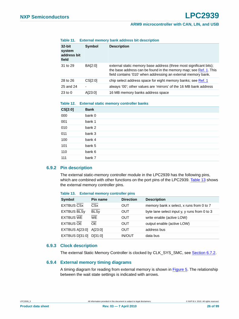
A separate chip select output is available for each bank. The chip select lines are configurable to be active HIGH or LOW. Memory bank selection is controlled by memory addressing. Table 11 shows how the 32-bit system address is mapped to the external bus memory base addresses, chip selects, and bank internal addresses.
LPC2939_3 All information provided in this document is subject to legal disclaimers. © NXP B.V. 2010. All rights reserved.
Product data sheet Rev. 03 — 7 April 2010 25 of 99
NXP Semiconductors LPC2939ARM9 microcontroller with CAN, LIN, and USB
6.9.2 Pin description
The external static-memory controller module in the LPC2939 has the following pins, which are combined with other functions on the port pins of the LPC2939. Table 13 shows the external memory controller pins.
6.9.3 Clock description
The external Static Memory Controller is clocked by CLK_SYS_SMC, see Section 6.7.2.
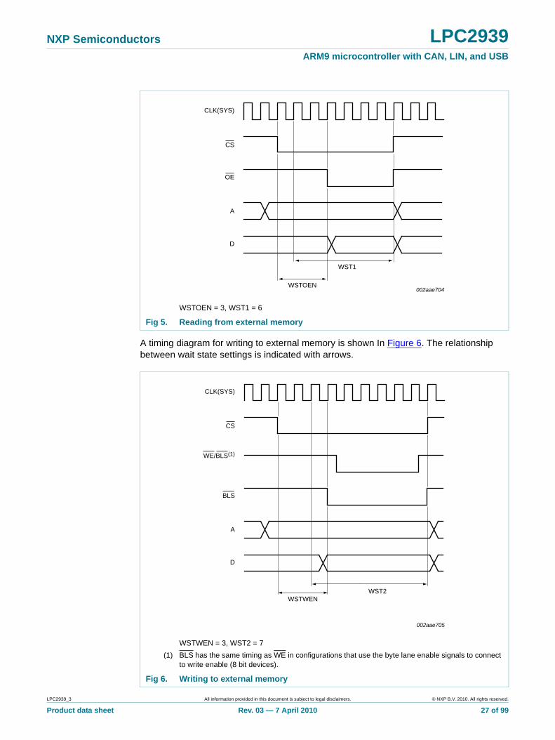
6.9.4 External memory timing diagrams
A timing diagram for reading from external memory is shown in Figure 5. The relationship between the wait state settings is indicated with arrows.
Table 11. External memory bank address bit description
32-bit system address bit field
Symbol Description
31 to 29 BA[2:0] external static memory base address (three most significant bits); the base address can be found in the memory map; see Ref. 1. This field contains ‘010’ when addressing an external memory bank.
28 to 26 CS[2:0] chip select address space for eight memory banks; see Ref. 1
25 and 24 - always ‘00’; other values are ‘mirrors’ of the 16 MB bank address
23 to 0 A[23:0] 16 MB memory banks address space
Table 12. External static memory controller banks
CS[2:0] Bank
000 bank 0
001 bank 1
010 bank 2
011 bank 3
100 bank 4
101 bank 5
110 bank 6
111 bank 7
Table 13. External memory controller pins
Symbol Pin name Direction Description
EXTBUS CSx CSx OUT memory bank x select, x runs from 0 to 7
EXTBUS BLSy BLSy OUT byte lane select input y, y runs from 0 to 3
EXTBUS WE WE OUT write enable (active LOW)
EXTBUS OE OE OUT output enable (active LOW)
EXTBUS A[23:0] A[23:0] OUT address bus
EXTBUS D[31:0] D[31:0] IN/OUT data bus
LPC2939_3 All information provided in this document is subject to legal disclaimers. © NXP B.V. 2010. All rights reserved.
Product data sheet Rev. 03 — 7 April 2010 26 of 99
NXP Semiconductors LPC2939ARM9 microcontroller with CAN, LIN, and USB
A timing diagram for writing to external memory is shown In Figure 6. The relationship between wait state settings is indicated with arrows.
WSTOEN = 3, WST1 = 6
Fig 5. Reading from external memory
WSTWEN = 3, WST2 = 7
(1) BLS has the same timing as WE in configurations that use the byte lane enable signals to connect to write enable (8 bit devices).
Fig 6. Writing to external memory
OE
CLK(SYS)
CS
A
D
WSTOEN
WST1
002aae704
BLS
CLK(SYS)
CS
A
D
WST2WSTWEN
002aae705
WE/BLS(1)
LPC2939_3 All information provided in this document is subject to legal disclaimers. © NXP B.V. 2010. All rights reserved.
Product data sheet Rev. 03 — 7 April 2010 27 of 99
NXP Semiconductors LPC2939ARM9 microcontroller with CAN, LIN, and USB
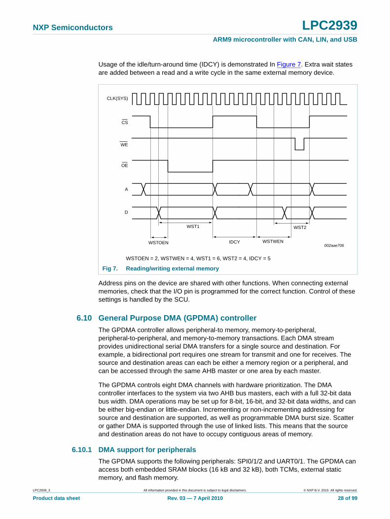
Usage of the idle/turn-around time (IDCY) is demonstrated In Figure 7. Extra wait states are added between a read and a write cycle in the same external memory device.
Address pins on the device are shared with other functions. When connecting external memories, check that the I/O pin is programmed for the correct function. Control of these settings is handled by the SCU.
6.10 General Purpose DMA (GPDMA) controller
The GPDMA controller allows peripheral-to memory, memory-to-peripheral, peripheral-to-peripheral, and memory-to-memory transactions. Each DMA stream provides unidirectional serial DMA transfers for a single source and destination. For example, a bidirectional port requires one stream for transmit and one for receives. The source and destination areas can each be either a memory region or a peripheral, and can be accessed through the same AHB master or one area by each master.
The GPDMA controls eight DMA channels with hardware prioritization. The DMA controller interfaces to the system via two AHB bus masters, each with a full 32-bit data bus width. DMA operations may be set up for 8-bit, 16-bit, and 32-bit data widths, and can be either big-endian or little-endian. Incrementing or non-incrementing addressing for source and destination are supported, as well as programmable DMA burst size. Scatter or gather DMA is supported through the use of linked lists. This means that the source and destination areas do not have to occupy contiguous areas of memory.
6.10.1 DMA support for peripherals
The GPDMA supports the following peripherals: SPI0/1/2 and UART0/1. The GPDMA can access both embedded SRAM blocks (16 kB and 32 kB), both TCMs, external static memory, and flash memory.
WSTOEN = 2, WSTWEN = 4, WST1 = 6, WST2 = 4, IDCY = 5
Fig 7. Reading/writing external memory
OE
CLK(SYS)
CS
A
D
WSTOEN
WST1
WSTWEN
WST2
IDCY002aae706
WE
LPC2939_3 All information provided in this document is subject to legal disclaimers. © NXP B.V. 2010. All rights reserved.
Product data sheet Rev. 03 — 7 April 2010 28 of 99
NXP Semiconductors LPC2939ARM9 microcontroller with CAN, LIN, and USB
6.10.2 Clock description
The DMA controller is clocked by CLK_SYS_DMA derived from BASE_SYS_CLK, see Section 6.7.2.
6.11 USB interface
The Universal Serial Bus (USB) is a 4-wire bus that supports communication between a host and one or more (up to 127) peripherals. The bus supports hot plugging and dynamic configuration of the devices. All transactions are initiated by the Host controller.
The LPC2939 USB interface includes a device and OTG controller with on-chip PHY for device. The OTG switching protocol is supported through the use of an external controller. Details on typical USB interfacing solutions can be found in Section 10.2.
6.11.1 USB device controller
The device controller enables 12 Mbit/s data exchange with a USB Host controller. It consists of a register interface, serial interface engine, endpoint buffer memory, and a DMA controller. The serial interface engine decodes the USB data stream and writes data to the appropriate endpoint buffer. The status of a completed USB transfer or error condition is indicated via status registers. An interrupt is also generated if enabled. When enabled, the DMA controller transfers data between the endpoint buffer and the on-chip SRAM.
The USB device controller has the following features:
• Fully compliant with USB 2.0 specification (full speed)
• Supports 32 physical (16 logical) endpoints with a 2 kB endpoint buffer RAM
• Supports Control, Bulk, Interrupt and Isochronous endpoints
• Scalable realization of endpoints at run time
• Endpoint Maximum packet size selection (up to USB maximum specification) by software at run time
• Supports SoftConnect and GoodLink features
• While USB is in the Suspend mode, the LPC2939 can enter the Power-down mode and wake up on USB activity
• Supports DMA transfers with the on-chip SRAM blocks on all non-control endpoints
• Allows dynamic switching between CPU-controlled slave and DMA modes
• Double buffer implementation for Bulk and Isochronous endpoints
6.11.2 USB OTG controller
USB OTG (On-The-Go) is a supplement to the USB 2.0 specification that augments the capability of existing mobile devices and USB peripherals by adding host functionality for connection to USB peripherals.
The OTG Controller integrates the device controller, and a master-only I2C interface to implement OTG dual-role device functionality. The dedicated I2C interface controls an external OTG transceiver.
The USB OTG controller has the following features:
LPC2939_3 All information provided in this document is subject to legal disclaimers. © NXP B.V. 2010. All rights reserved.
Product data sheet Rev. 03 — 7 April 2010 29 of 99
NXP Semiconductors LPC2939ARM9 microcontroller with CAN, LIN, and USB
• Fully compliant with On-The-Go supplement to the USB 2.0 Specification, Revision 1.0a
• Hardware support for Host Negotiation Protocol (HNP)
• Includes a programmable timer required for HNP and Session Request Protocol (SRP)
• Supports any OTG transceiver compliant with the OTG Transceiver Specification (CEA-2011), Rev. 1.0
6.11.3 USB host controller
The host controller enables full- and low-speed data exchange with USB devices attached to the bus. It consists of register interface, serial interface engine and DMA controller. The register interface complies with the OHCI specification.
6.11.3.1 Features
• OHCI compliant
• Two downstream ports
• Supports per-port power switching
6.11.4 Pin description
Table 14. USB OTG port pins
Pin name Direction Description Interfacing
Port 1
USB_VBUS1 I VBUS status input. When this function is not enabled via its corresponding PINSEL register, it is driven HIGH internally.
-
USB_D+1 I/O positive differential data -
USB_D1 I/O negative differential data -
USB_CONNECT1 O SoftConnect control signal -
USB_UP_LED1 O GoodLink LED control signal -
USB_SCL1 I/O I2C serial clock external OTG transceiver
USB_SDA1 I/O I2C serial data external OTG transceiver
USB_LS1 O low-speed status (applies to host functionality only) external OTG transceiver
USB_RST1 O USB reset status external OTG transceiver
USB_INT1 O USB transceiver interrupt external OTG transceiver
USB_SSPND1 O bus suspend status external OTG transceiver
USB_PWRD1 I port power status USB host
USB_PPWR1 O port power enable USB host
USB_OVRCR1 I over-current status USB host
Port 2
USB_VBUS2 I VBUS status input. When this function is not enabled via its corresponding PINSEL register, it is driven HIGH internally.
-
USB_D+2 I/O positive differential data -
USB_D2 I/O negative differential data -
LPC2939_3 All information provided in this document is subject to legal disclaimers. © NXP B.V. 2010. All rights reserved.
Product data sheet Rev. 03 — 7 April 2010 30 of 99
NXP Semiconductors LPC2939ARM9 microcontroller with CAN, LIN, and USB
6.11.5 Clock description
Access to the USB registers is clocked by the CLK_SYS_USB, derived from BASE_SYS_CLK, see Section 6.7.2. The CGU1 provides two independent base clocks to the USB block, BASE_USB_CLK and BASE_USB_I2C_CLK (see Section 6.16.3).
6.12 General subsystem
6.12.1 General subsystem clock description
The general subsystem is clocked by CLK_SYS_GESS, see Section 6.7.2.
6.12.2 Chip and feature identification
The Chip/Feature ID (CFID) module contains registers which show and control the functionality of the chip. It contains an ID to identify the silicon and also registers containing information about the features enabled or disabled on the chip.
The key features are:
• Identification of product
• Identification of features enabled
The CFID has no external pins.
6.12.3 System Control Unit (SCU)
The system control unit contains system related functions.The key feature is configuration of the I/O port pins multiplexer. It defines the function of each I/O pin of the LPC2939. The I/O pin configuration should be consistent with peripheral function usage.
The SCU has no external pins.
6.12.4 Event router
The event router provides bus-controlled routing of input events to the vectored interrupt controller for use as interrupt or wake-up signals.
Key features:
• Up to 22 level-sensitive external interrupt pins, including the receive pins of SPI, CAN, LIN, USB, and UART, as well as the I2C-bus SCL pins plus three internal event sources
• Input events can be used as interrupt source either directly or latched (edge-detected)
• Direct events disappear when the event becomes inactive
• Latched events remain active until they are explicitly cleared
USB_CONNECT2 O SoftConnect control signal -
USB_UP_LED2 O GoodLink LED control signal -
USB_PWRD2 I port power status USB host
USB_PPWR2 O port power enable USB host
USB_OVRCR2 I over-current status USB host
Table 14. USB OTG port pins …continued
Pin name Direction Description Interfacing
LPC2939_3 All information provided in this document is subject to legal disclaimers. © NXP B.V. 2010. All rights reserved.
Product data sheet Rev. 03 — 7 April 2010 31 of 99
NXP Semiconductors LPC2939ARM9 microcontroller with CAN, LIN, and USB
• Programmable input level and edge polarity
• Event detection maskable
• Event detection is fully asynchronous, so no clock is required
The event router allows the event source to be defined, its polarity and activation type to be selected and the interrupt to be masked or enabled. The event router can be used to start a clock on an external event.
The vectored interrupt controller inputs are active HIGH.
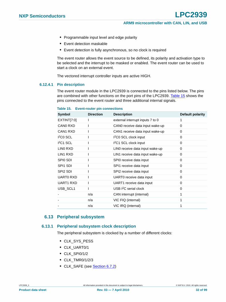
6.12.4.1 Pin description
The event router module in the LPC2939 is connected to the pins listed below. The pins are combined with other functions on the port pins of the LPC2939. Table 15 shows the pins connected to the event router and three additional internal signals.
6.13 Peripheral subsystem
6.13.1 Peripheral subsystem clock description
The peripheral subsystem is clocked by a number of different clocks:
• CLK_SYS_PESS
• CLK_UART0/1
• CLK_SPI0/1/2
• CLK_TMR0/1/2/3
• CLK_SAFE (see Section 6.7.2)
Table 15. Event-router pin connections
Symbol Direction Description Default polarity
EXTINT[7:0] I external interrupt inputs 7 to 0 1
CAN0 RXD I CAN0 receive data input wake-up 0
CAN1 RXD I CAN1 receive data input wake-up 0
I2C0 SCL I I2C0 SCL clock input 0
I2C1 SCL I I2C1 SCL clock input 0
LIN0 RXD I LIN0 receive data input wake-up 0
LIN1 RXD I LIN1 receive data input wake-up 0
SPI0 SDI I SPI0 receive data input 0
SPI1 SDI I SPI1 receive data input 0
SPI2 SDI I SPI2 receive data input 0
UART0 RXD I UART0 receive data input 0
UART1 RXD I UART1 receive data input 0
USB_SCL1 I USB I2C serial clock 0
- n/a CAN interrupt (internal) 1
- n/a VIC FIQ (internal) 1
- n/a VIC IRQ (internal) 1
LPC2939_3 All information provided in this document is subject to legal disclaimers. © NXP B.V. 2010. All rights reserved.
Product data sheet Rev. 03 — 7 April 2010 32 of 99
NXP Semiconductors LPC2939ARM9 microcontroller with CAN, LIN, and USB
6.13.2 Watchdog timer
The purpose of the watchdog timer is to reset the ARM9 processor within a reasonable amount of time if the processor enters an error state. The watchdog generates a system reset if the user program fails to trigger it correctly within a predetermined amount of time.
Key features:
• Internal chip reset if not periodically triggered
• Timer counter register runs on always-on safe clock
• Optional interrupt generation on watchdog time-out
• Debug mode with disabling of reset
• Watchdog control register change protected with key
• Programmable 32-bit watchdog timer period with programmable 32-bit prescaler
6.13.2.1 Functional description
The watchdog timer consists of a 32-bit counter with a 32-bit prescaler.
The watchdog should be programmed with a time-out value and then periodically restarted. When the watchdog times out, it generates a reset through the RGU.
To generate watchdog interrupts in watchdog debug mode the interrupt has to be enabled via the interrupt enable register. A watchdog overflow interrupt can be cleared by writing to the clear-interrupt register.
Another way to prevent resets during debug mode is via the Pause feature of the watchdog timer. The watchdog is stalled when the ARM9 is in debug mode and the PAUSE_ENABLE bit in the watchdog timer control register is set.
The Watchdog Reset output is fed to the Reset Generator Unit (RGU). The RGU contains a reset source register to identify the reset source when the device has gone through a reset. See Section 6.16.4.
6.13.2.2 Clock description
The watchdog timer is clocked by two different clocks; CLK_SYS_PESS and CLK_SAFE, see Section 6.7.2. The register interface towards the system bus is clocked by CLK_SYS_PESS. The timer and prescale counters are clocked by CLK_SAFE which is always on.
6.13.3 Timer
The LPC2939 contains six identical timers: four in the peripheral subsystem and two in the Modulation and Sampling Control SubSystem (MSCSS) located at different peripheral base addresses. This section describes the four timers in the peripheral subsystem. Each timer has four capture inputs and/or match outputs. Connection to device pins depends on the configuration programmed into the port function-select registers. The two timers located in the MSCSS have no external capture or match pins, but the memory map is identical, see Section 6.15.6. One of these timers has an external input for a pause function.
LPC2939_3 All information provided in this document is subject to legal disclaimers. © NXP B.V. 2010. All rights reserved.
Product data sheet Rev. 03 — 7 April 2010 33 of 99
NXP Semiconductors LPC2939ARM9 microcontroller with CAN, LIN, and USB
The key features are:
• 32-bit timer/counter with programmable 32-bit prescaler
• Up to four 32-bit capture channels per timer. These take a snapshot of the timer value when an external signal connected to the TIMERx CAPn input changes state. A capture event may also optionally generate an interrupt.
• Four 32-bit match registers per timer that allow:
– Continuous operation with optional interrupt generation on match
– Stop timer on match with optional interrupt generation
– Reset timer on match with optional interrupt generation
• Up to four external outputs per timer corresponding to match registers, with the following capabilities:
– Set LOW on match
– Set HIGH on match
– Toggle on match
– Do nothing on match
• Pause input pin (MSCSS timers only)
The timers are designed to count cycles of the clock and optionally generate interrupts or perform other actions at specified timer values, based on four match registers. They also include capture inputs to trap the timer value when an input signal changes state, optionally generating an interrupt. The core function of the timers consists of a 32 bit prescale counter triggering the 32 bit timer counter. Both counters run on clock CLK_TMRx (x runs from 0 to 3) and all time references are related to the period of this clock. Note that each timer has its individual clock source within the Peripheral SubSystem. In the Modulation and Sampling SubSystem each timer also has its own individual clock source. See Section 6.16.5 for information on generation of these clocks.
6.13.3.1 Pin description
The four timers in the peripheral subsystem of the LPC2939 have the pins described below. The two timers in the modulation and sampling subsystem have no external pins except for the pause pin on MSCSS timer 1. See Section 6.15.6 for a description of these timers and their associated pins. The timer pins are combined with other functions on the port pins of the LPC2939, see Section 6.12.3. Table 16 shows the timer pins (x runs from 0 to 3).
Table 16. Timer pins
Symbol Pin names Direction Description
TIMERx CAP[0] CAPx[0] IN TIMER x capture input 0
TIMERx CAP[1] CAPx[1] IN TIMER x capture input 1
TIMERx CAP[2] CAPx[2] IN TIMER x capture input 2
TIMERx CAP[3] CAPx[3] IN TIMER x capture input 3
TIMERx MAT[0] MATx[0] OUT TIMER x match output 0
TIMERx MAT[1] MATx[1] OUT TIMER x match output 1
TIMERx MAT[2] MATx[2] OUT TIMER x match output 2
TIMERx MAT[3] MATx[3] OUT TIMER x match output 3
LPC2939_3 All information provided in this document is subject to legal disclaimers. © NXP B.V. 2010. All rights reserved.
Product data sheet Rev. 03 — 7 April 2010 34 of 99
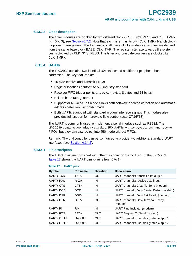
NXP Semiconductors LPC2939ARM9 microcontroller with CAN, LIN, and USB
6.13.3.2 Clock description
The timer modules are clocked by two different clocks; CLK_SYS_PESS and CLK_TMRx (x = 0 to 3), see Section 6.7.2. Note that each timer has its own CLK_TMRx branch clock for power management. The frequency of all these clocks is identical as they are derived from the same base clock BASE_CLK_TMR. The register interface towards the system bus is clocked by CLK_SYS_PESS. The timer and prescale counters are clocked by CLK_TMRx.
6.13.4 UARTs
The LPC2939 contains two identical UARTs located at different peripheral base addresses. The key features are:
• 16-byte receive and transmit FIFOs
• Register locations conform to 550 industry standard
• Receiver FIFO trigger points at 1 byte, 4 bytes, 8 bytes and 14 bytes
• Built-in baud rate generator
• Support for RS-485/9-bit mode allows both software address detection and automatic address detection using 9-bit mode
• Both UARTs equipped with standard modem interface signals. This module also provides full support for hardware flow control (auto-CTS/RTS)
The UART is commonly used to implement a serial interface such as RS232. The LPC2939 contains two industry-standard 550 UARTs with 16-byte transmit and receive FIFOs, but they can also be put into 450 mode without FIFOs.
Remark: The LIN controller can be configured to provide two additional standard UART interfaces (see Section 6.14.2).
6.13.4.1 Pin description
The UART pins are combined with other functions on the port pins of the LPC2939. Table 17 shows the UART pins (x runs from 0 to 1).
Table 17. UART pins
Symbol Pin name Direction Description
UARTx TXD TXDx OUT UART channel x transmit data output
UARTx RXD RXDx IN UART channel x receive data input
UARTx CTS CTSx IN UART channel x Clear To Send (modem)
UARTx DCD DCDx IN UART channel x Data Carrier Detect (modem)
UARTx DSR DSRx IN UART channel x Data Set Ready (modem)
UARTx DTR DTRx OUT UART channel x Data Terminal Ready (modem)
UARTx RI RIx IN UART Ring Indicator (modem)
UARTx RTS RTSx OUT UART Request To Send (modem)
UARTx OUT1 UxOUT1 OUT UART channel x user designated output 1
UARTx OUT2 UxOUT2 OUT UART channel x user designated output 2
LPC2939_3 All information provided in this document is subject to legal disclaimers. © NXP B.V. 2010. All rights reserved.
Product data sheet Rev. 03 — 7 April 2010 35 of 99
NXP Semiconductors LPC2939ARM9 microcontroller with CAN, LIN, and USB
6.13.4.2 Clock description
The UART modules are clocked by two different clocks; CLK_SYS_PESS and CLK_UARTx (x = 0 to 1), see Section 6.7.2. Note that each UART has its own CLK_UARTx branch clock for power management. The frequency of all CLK_UARTx clocks is identical since they are derived from the same base clock BASE_CLK_UART. The register interface towards the system bus is clocked by CLK_SYS_PESS. The baud generator is clocked by the CLK_UARTx.
6.13.5 Serial peripheral interface (SPI)
The LPC2939 contains three Serial Peripheral Interface modules (SPIs) to allow synchronous serial communication with slave or master peripherals.
The key features are:
• Master or slave operation
• Each SPI supports up to four slaves in sequential multi-slave operation
• Supports timer-triggered operation
• Programmable clock bit rate and prescale based on SPI source clock (BASE_SPI_CLK), independent of system clock
• Separate transmit and receive FIFO memory buffers; 16 bits wide, 32 locations deep
• Programmable choice of interface operation: Motorola SPI or Texas Instruments Synchronous Serial Interfaces
• Programmable data-frame size from 4 to 16 bits
• Independent masking of transmit FIFO, receive FIFO and receive overrun interrupts
• Serial clock-rate master mode: fserial_clk fclk(SPI) / 2
• Serial clock-rate slave mode: fserial_clk = fclk(SPI) / 4
• Internal loopback test mode
The SPI module can operate in:
• Master mode:
– Normal transmission mode
– Sequential slave mode
• Slave mode
6.13.5.1 Functional description
The SPI module is a master or slave interface for synchronous serial communication with peripheral devices that have either Motorola SPI or Texas Instruments Synchronous Serial Interfaces.
The SPI module performs serial-to-parallel conversion on data received from a peripheral device. The transmit and receive paths are buffered with FIFO memories (16 bits wide 32 words deep). Serial data is transmitted on pins SDOx and received on pins SDIx.
The SPI module includes a programmable bit-rate clock divider and prescaler to generate the SPI serial clock from the input clock CLK_SPIx.
LPC2939_3 All information provided in this document is subject to legal disclaimers. © NXP B.V. 2010. All rights reserved.
Product data sheet Rev. 03 — 7 April 2010 36 of 99
NXP Semiconductors LPC2939ARM9 microcontroller with CAN, LIN, and USB
The SPI module’s operating mode, frame format, and word size are programmed through the SLVn_SETTINGS registers.
A single combined interrupt request SPI_INTREQ output is asserted if any of the interrupts are asserted and unmasked.
Depending on the operating mode selected, the SPI SCS outputs operate as an active-HIGH frame synchronization output for Texas Instruments synchronous serial frame format or an active-LOW chip select for SPI.
Each data frame is between four and 16 bits long, depending on the size of words programmed, and is transmitted starting with the MSB.
6.13.5.2 Pin description
The SPI pins are combined with other functions on the port pins of the LPC2939, see Section 6.12.3. Table 18 shows the SPI pins (x runs from 0 to 2; y runs from 0 to 3).
[1] Direction of SPIx SCS and SPIx SCK pins depends on master or slave mode. These pins are output in master mode, input in slave mode.
[2] In slave mode there is only one chip select input pin, SPIx SCS0. The other chip selects have no function in slave mode.
6.13.5.3 Clock description
The SPI modules are clocked by two different clocks; CLK_SYS_PESS and CLK_SPIx (x = 0, 1, 2), see Section 6.7.2. Note that each SPI has its own CLK_SPIx branch clock for power management. The frequency of all clocks CLK_SPIx is identical as they are derived from the same base clock BASE_CLK_SPI. The register interface towards the system bus is clocked by CLK_SYS_PESS. The serial-clock rate divisor is clocked by CLK_SPIx.
The SPI clock frequency can be controlled by the CGU. In master mode the SPI clock frequency (CLK_SPIx) must be set to at least twice the SPI serial clock rate on the interface. In slave mode CLK_SPIx must be set to four times the SPI serial clock rate on the interface.
6.13.6 General-Purpose I/O (GPIO)
The LPC2939 contains six general-purpose I/O ports located at different peripheral base addresses. In the 208-pin package all six ports are available. All I/O pins are bidirectional, and the direction can be programmed individually. The I/O pad behavior depends on the configuration programmed in the port function-select registers.
The key features are:
• General-purpose parallel inputs and outputs
• Direction control of individual bits
• Synchronized input sampling for stable input data values
Table 18. SPI pins
Symbol Pin name Direction Description
SPIx SCSy SCSx[y] IN/OUT SPIx chip select[1][2]
SPIx SCK SCKx IN/OUT SPIx clock[1]
SPIx SDI SDIx IN SPIx data input
SPIx SDO SDOx OUT SPIx data output
LPC2939_3 All information provided in this document is subject to legal disclaimers. © NXP B.V. 2010. All rights reserved.
Product data sheet Rev. 03 — 7 April 2010 37 of 99
NXP Semiconductors LPC2939ARM9 microcontroller with CAN, LIN, and USB
• All I/O pins default to input at reset to avoid any possible bus conflicts
6.13.6.1 Functional description
The general-purpose I/O provides individual control over each bidirectional port pin. There are two registers to control I/O direction and output level. The inputs are synchronized to achieve stable read levels.
To generate an open-drain output, set the bit in the output register to the desired value. Use the direction register to control the signal. When set to output, the output driver actively drives the value on the output; when set to input the signal floats and can be pulled up internally or externally.
6.13.6.2 Pin description
The six GPIO ports in the LPC2939 have the pins listed below. The GPIO pins are combined with other functions on the port pins of the LPC2939. Table 19 shows the GPIO pins.
6.13.6.3 Clock description
The GPIO modules are clocked by several clocks, all of which are derived from BASE_SYS_CLK; CLK_SYS_PESS and CLK_SYS_GPIOx (x = 0, 1, 2, 3, 4, 5), see Section 6.7.2. Note that each GPIO has its own CLK__SYS_GPIOx branch clock for power management. The frequency of all clocks CLK_SYS_GPIOx is identical to CLK_SYS_PESS since they are derived from the same base clock BASE_SYS_CLK.
6.14 Networking subsystem
6.14.1 CAN gateway
Controller Area Network (CAN) is the definition of a high-performance communication protocol for serial data communication. The two CAN controllers in the LPC2939 provide a full implementation of the CAN protocol according to the CAN specification version 2.0B. The gateway concept is fully scalable with the number of CAN controllers, and always operates together with a separate powerful and flexible hardware acceptance filter.
The key features are:
• Supports 11-bit as well as 29-bit identifiers
• Double receive buffer and triple transmit buffer
• Programmable error-warning limit and error counters with read/write access
• Arbitration-lost capture and error-code capture with detailed bit position
• Single-shot transmission (i.e. no re-transmission)
Table 19. GPIO pins
Symbol Pin name Direction Description
GPIO0 pin[31:0] P0[31:0] IN/OUT GPIO port x pins 31 to 0
GPIO1 pin[31:0] P1[31:0] IN/OUT GPIO port x pins 31 to 0
GPIO2 pin[27:0] P2[27:0] IN/OUT GPIO port x pins 27 to 0
GPIO3 pin[15:0] P3[15:0] IN/OUT GPIO port x pins 15 to 0
GPIO4 pin[23:0] P4[23:0] IN/OUT GPIO port x pins 23 to 0
GPIO5 pin[19:0] P5[19:0] IN/OUT GPIO port x pins 19 to 0
LPC2939_3 All information provided in this document is subject to legal disclaimers. © NXP B.V. 2010. All rights reserved.
Product data sheet Rev. 03 — 7 April 2010 38 of 99
NXP Semiconductors LPC2939ARM9 microcontroller with CAN, LIN, and USB
• Listen-only mode (no acknowledge; no active error flags)
• Reception of ‘own’ messages (self-reception request)
• Full CAN mode for message reception
6.14.1.1 Global acceptance filter
The global acceptance filter provides look-up of received identifiers - called acceptance filtering in CAN terminology - for all the CAN controllers. It includes a CAN ID look-up table memory, in which software maintains one to five sections of identifiers. The CAN ID look-up table memory is 2 kB large (512 words, each of 32 bits). It can contain up to 1024 standard frame identifiers or 512 extended frame identifiers or a mixture of both types. It is also possible to define identifier groups for standard and extended message formats.
6.14.1.2 Pin description
The two CAN controllers in the LPC2939 have the pins listed below. The CAN pins are combined with other functions on the port pins of the LPC2939. Table 20 shows the CAN pins (x runs from 0 to 1).
6.14.2 LIN
The LPC2939 contain two LIN 2.0 master controllers. These can be used as dedicated LIN 2.0 master controllers with additional support for sync break generation and with hardware implementation of the LIN protocol according to spec 2.0.
Remark: Both LIN channels can be also configured as UART channels.
The key features are:
• Complete LIN 2.0 message handling and transfer
• One interrupt per LIN message
• Slave response time-out detection
• Programmable sync-break length
• Automatic sync-field and sync-break generation
• Programmable inter-byte space
• Hardware or software parity generation
• Automatic checksum generation
• Fault confinement
• Fractional baud rate generator
6.14.2.1 Pin description
The two LIN 2.0 master controllers in the LPC2939 have the pins listed below. The LIN pins are combined with other functions on the port pins of the LPC2939. Table 21 shows the LIN pins. For more information see Ref. 1 subsection 3.43, LIN master controller.
Table 20. CAN pins
Symbol Pin name Direction Description
CANx TXD TXDC0/1 OUT CAN channel x transmit data output
CANx RXD RXDC0/1 IN CAN channel x receive data input
LPC2939_3 All information provided in this document is subject to legal disclaimers. © NXP B.V. 2010. All rights reserved.
Product data sheet Rev. 03 — 7 April 2010 39 of 99
NXP Semiconductors LPC2939ARM9 microcontroller with CAN, LIN, and USB
6.14.3 I2C-bus serial I/O controllers
The LPC2939 each contain two I2C-bus controllers.
The I2C-bus is bidirectional for inter-IC control using only two wires: a serial clock line (SCL) and a serial data line (SDA). Each device is recognized by a unique address and can operate as either a receiver-only device (e.g., an LCD driver) or as a transmitter with the capability to both receive and send information (such as memory). Transmitters and/or receivers can operate in either master or slave mode, depending on whether the chip has to initiate a data transfer or is only addressed. The I2C is a multi-master bus, and it can be controlled by more than one bus master connected to it.
The main features if the I2C-bus interfaces are:
• I2C0 and I2C1 use standard I/O pins with bit rates of up to 400 kbit/s (Fast I2C-bus) and do not support powering off of individual devices connected to the same bus lines
• Easy to configure as master, slave, or master/slave
• Programmable clocks allow versatile rate control
• Bidirectional data transfer between masters and slaves
• Multi-master bus (no central master)
• Arbitration between simultaneously transmitting masters without corruption of serial data on the bus
• Serial clock synchronization allows devices with different bit rates to communicate via one serial bus
• Serial clock synchronization can be used as a handshake mechanism to suspend and resume serial transfer
• The I2C-bus can be used for test and diagnostic purposes
• All I2C-bus controllers support multiple address recognition and a bus monitor mode
6.14.3.1 Pin description
[1] Note that the pins are not I2C-bus compliant open-drain pins.
6.15 Modulation and Sampling Control SubSystem (MSCSS)
The Modulation and Sampling Control Subsystem (MSCSS) in the LPC2939 includes four Pulse-Width Modulators (PWMs), three 10-bit successive approximation Analog-to-Digital Converters (ADCs) and two timers.
The key features of the MSCSS are:
Table 21. LIN controller pins
Symbol Pin name Direction Description
LIN0/1 TXD TXDL0/1 OUT LIN channel 0/1 transmit data output
LIN0/1 RXD RXDL0/1 IN LIN channel 0/1 receive data input
Table 22. I2C-bus pins [1]
Symbol Pin name Direction Description
I2C SCL0/1 SCL0/1 I/O I2C clock input/output
I2C SDA0/1 SDA0/1 I/O I2C data input/output
LPC2939_3 All information provided in this document is subject to legal disclaimers. © NXP B.V. 2010. All rights reserved.
Product data sheet Rev. 03 — 7 April 2010 40 of 99
NXP Semiconductors LPC2939ARM9 microcontroller with CAN, LIN, and USB
• Two 10-bit, 400 ksamples/s, 8-channel ADCs with 3.3 V inputs and various trigger- start options
• One 10-bit, 400 ksamples/s, 8-channel ADC with 5 V inputs (5 V measurement range) and various trigger-start options
• Four 6-channel PWMs (Pulse-Width Modulators) with capture and trap functionality
• Two dedicated timers to schedule and synchronize the PWMs and ADCs
• Quadrature encoder interface
6.15.1 Functional description
The MSCSS contains Pulse-Width Modulators (PWMs), Analog-to-Digital Converters (ADCs) and timers.
Figure 8 provides an overview of the MSCSS. An AHB-to-APB bus bridge takes care of communication with the AHB system bus. Two internal timers are dedicated to this subsystem. MSCSS timer 0 can be used to generate start pulses for the ADCs and the first PWM. The second timer (MSCSS timer 1) is used to generate ‘carrier’ signals for the PWMs. These carrier patterns can be used, for example, in applications requiring current control. Several other trigger possibilities are provided for the ADCs (external, cascaded or following a PWM). The capture inputs of both timers can also be used to capture the start pulse of the ADCs.
The PWMs can be used to generate waveforms in which the frequency, duty cycle and rising and falling edges can be controlled very precisely. Capture inputs are provided to measure event phases compared to the main counter. Depending on the applications, these inputs can be connected to digital sensor motor outputs or digital external signals. Interrupt signals are generated on several events to closely interact with the CPU.
The ADCs can be used for any application needing accurate digitized data from analog sources. To support applications like motor control, a mechanism to synchronize several PWMs and ADCs is available (sync_in and sync_out).
Note that the PWMs run on the PWM clock and the ADCs on the ADC clock, see Section 6.16.2.
LPC2939_3 All information provided in this document is subject to legal disclaimers. © NXP B.V. 2010. All rights reserved.
Product data sheet Rev. 03 — 7 April 2010 41 of 99
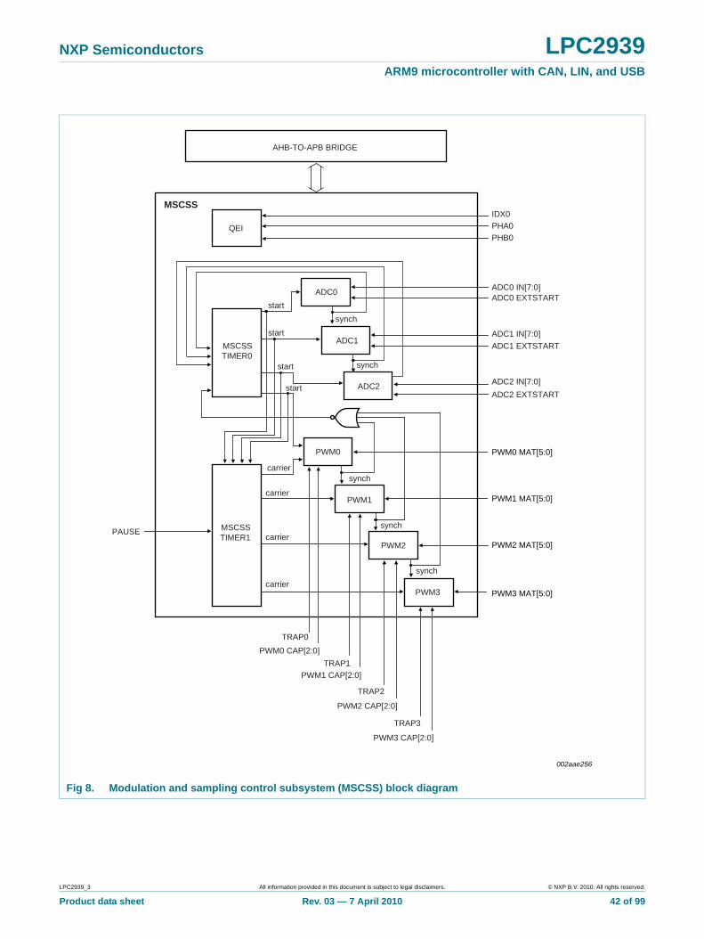
NXP Semiconductors LPC2939ARM9 microcontroller with CAN, LIN, and USB
Fig 8. Modulation and sampling control subsystem (MSCSS) block diagram
002aae256
PWM0 MAT[5:0]
PWM1 MAT[5:0]
PWM2 MAT[5:0]
PWM3 MAT[5:0]
PWM0 CAP[2:0]
PAUSE
MSCSSTIMER0
MSCSSTIMER1
ADC0
ADC1
ADC2
PWM0
PWM1
ADC0 IN[7:0]
ADC1 IN[7:0]
ADC2 IN[7:0]
ADC2 EXTSTART
QEI
PWM1 CAP[2:0]
TRAP2
TRAP0
TRAP1
PWM2 CAP[2:0]
TRAP3
PWM3 CAP[2:0]
ADC1 EXTSTART
ADC0 EXTSTARTstart
start
start
start
synch
synch
synch
PWM2
synch
PWM3
synch
carrier
carrier
carrier
carrier
IDX0PHA0PHB0
MSCSS
AHB-TO-APB BRIDGE
LPC2939_3 All information provided in this document is subject to legal disclaimers. © NXP B.V. 2010. All rights reserved.
Product data sheet Rev. 03 — 7 April 2010 42 of 99
NXP Semiconductors LPC2939ARM9 microcontroller with CAN, LIN, and USB
6.15.2 Pin description
The pins of the LPC2939 MSCSS associated with the three ADC modules are described in Section 6.15.4.2. Pins connected to the four PWM modules are described in Section 6.15.5.4, pins directly connected to the MSCSS timer 1 module are described in Section 6.15.6.1, and pins connected to the quadrature encoder interface are described in Section 6.15.7.1.
6.15.3 Clock description
The MSCSS is clocked from a number of different sources:
• CLK_SYS_MSCSS_A clocks the AHB side of the AHB-to-APB bus bridge
• CLK_MSCSS_APB clocks the subsystem APB bus
• CLK_MSCSS_MTMR0/1 clocks the timers
• CLK_MSCSS_PWM0:3 clocks the PWMs
Each ADC has two clock areas; a APB part clocked by CLK_MSCSS_ADCx_APB (x = 0, 1, or 2) and a control part for the analog section clocked by CLK_ADCx = 0, 1, or 2), see Section 6.7.2.
All clocks are derived from the BASE_MSCSS_CLK, except for CLK_SYS_MSCSS_A which is derived form BASE_SYS_CLK, and the CLK_ADCx clocks which are derived from BASE_CLK_ADC. If specific PWM or ADC modules are not used their corresponding clocks can be switched off.
6.15.4 Analog-to-digital converter
The MSCSS in the LPC2939 includes three 10-bit successive-approximation analog-to-digital converters.
The key features of the ADC interface module are:
• ADC0: Eight analog inputs; time-multiplexed; measurement range up to 5.0 V
• ADC1 and ADC2: Eight analog inputs; time-multiplexed; measurement range up to 3.3 V
• External reference-level inputs
• 400 ksamples/s at 10-bit resolution up to 1500 ksamples/s at 2-bit resolution
• Programmable resolution from 2-bit to10-bit
• Single analog-to-digital conversion scan mode and continuous analog-to-digital conversion scan mode
• Optional conversion on transition on external start input, timer capture/match signal, PWM_sync or ‘previous’ ADC
• Converted digital values are stored in a register for each channel
• Optional compare condition to generate a ‘less than’ or an ‘equal to or greater than’ compare-value indication for each channel
• Power-down mode
LPC2939_3 All information provided in this document is subject to legal disclaimers. © NXP B.V. 2010. All rights reserved.
Product data sheet Rev. 03 — 7 April 2010 43 of 99
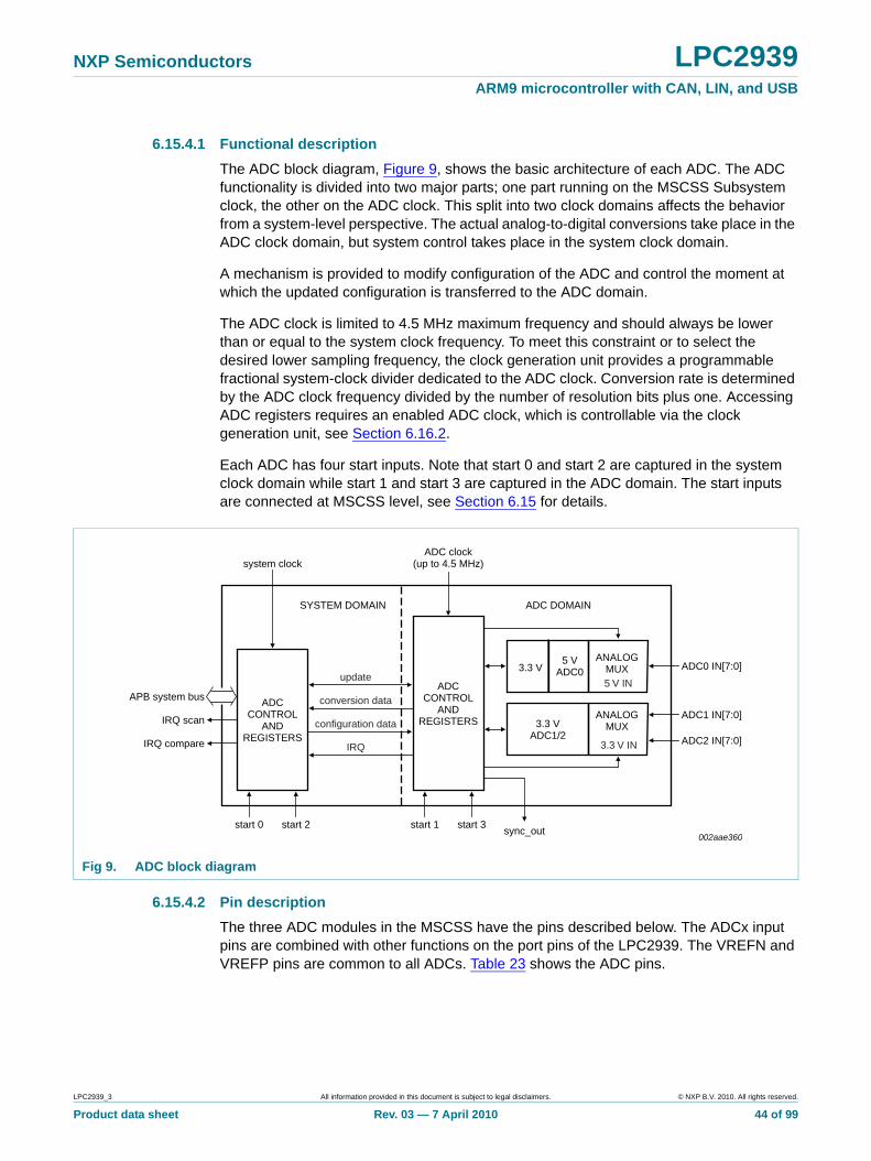
NXP Semiconductors LPC2939ARM9 microcontroller with CAN, LIN, and USB
6.15.4.1 Functional description
The ADC block diagram, Figure 9, shows the basic architecture of each ADC. The ADC functionality is divided into two major parts; one part running on the MSCSS Subsystem clock, the other on the ADC clock. This split into two clock domains affects the behavior from a system-level perspective. The actual analog-to-digital conversions take place in the ADC clock domain, but system control takes place in the system clock domain.
A mechanism is provided to modify configuration of the ADC and control the moment at which the updated configuration is transferred to the ADC domain.
The ADC clock is limited to 4.5 MHz maximum frequency and should always be lower than or equal to the system clock frequency. To meet this constraint or to select the desired lower sampling frequency, the clock generation unit provides a programmable fractional system-clock divider dedicated to the ADC clock. Conversion rate is determined by the ADC clock frequency divided by the number of resolution bits plus one. Accessing ADC registers requires an enabled ADC clock, which is controllable via the clock generation unit, see Section 6.16.2.
Each ADC has four start inputs. Note that start 0 and start 2 are captured in the system clock domain while start 1 and start 3 are captured in the ADC domain. The start inputs are connected at MSCSS level, see Section 6.15 for details.
6.15.4.2 Pin description
The three ADC modules in the MSCSS have the pins described below. The ADCx input pins are combined with other functions on the port pins of the LPC2939. The VREFN and VREFP pins are common to all ADCs. Table 23 shows the ADC pins.
Fig 9. ADC block diagram
002aae360start 2start 0
system clockADC clock
(up to 4.5 MHz)
APB system bus
IRQ scan
IRQ compare
ADC1 IN[7:0]
ADC2 IN[7:0]
start 1 start 3sync_out
ADC DOMAINSYSTEM DOMAIN
ADCCONTROL
ANDREGISTERS
ADCCONTROL
ANDREGISTERS
3.3 VADC1/2
ANALOGMUX
conversion data
update
configuration data
IRQ
ADC0 IN[7:0]5 VADC03.3 V
ANALOGMUX5 V IN
3.3 V IN
LPC2939_3 All information provided in this document is subject to legal disclaimers. © NXP B.V. 2010. All rights reserved.
Product data sheet Rev. 03 — 7 April 2010 44 of 99
NXP Semiconductors LPC2939ARM9 microcontroller with CAN, LIN, and USB
[1] VREFP, VREFN, VDDA(ADC3V3) must be connected for the 5 V ADC0 to operate properly.
[2] The analog inputs of ADC0 are internally multiplied by a factor of 3.3 / 5. If VDDA(ADC5V0) is connected to 3.3 V, the maximum digital result is 1024 3.3 / 5.
[3] VDDA(ADC5V0) and VDDA(ADC3V3) must be set as follows: VDDA(ADC5V0) = VDDA(ADC3V3) 1.5.
Remark: The following formula only applies to ADC0:
Voltage variations on VREFP (i.e. those that deviate from voltage variations on the VDDA(ADC5V5) pin) are visible as variations in the measurement result. Equation 3 shows the formula used to determine the conversion result of an input voltage VIN on ADC0:
(3)
Remark: Note that the ADC1 and ADC2 accept an input voltage up to of 3.6 V (see Table 34) on the ADC1/2 IN pins. If the ADC is not used, the pins are 5 V tolerant. The ADC0 pins are 5 V tolerant.
6.15.4.3 Clock description
The ADC modules are clocked from two different sources; CLK_MSCSS_ADCx_APB and CLK_ADCx (x = 0, 1, or 2), see Section 6.7.2. Note that each ADC has its own CLK_ADCx and CLK_MSCSS_ADCx_APB branch clocks for power management. If an ADC is unused both its CLK_MSCSS_ADCx_APB and CLK_ADCx can be switched off.
The frequency of all the CLK_MSCSS_ADCx_APB clocks is identical to CLK_MSCSS_APB since they are derived from the same base clock BASE_MSCSS_CLK. Likewise the frequency of all the CLK_ADCx clocks is identical since they are derived from the same base clock BASE_ADC_CLK.
The register interface towards the system bus is clocked by CLK_MSCSS_ADCx_APB. Control logic for the analog section of the ADC is clocked by CLK_ADCx, see also Figure 9.
6.15.5 Pulse Width Modulator (PWM)
The MSCSS in the LPC2939 includes four PWM modules with the following features.
Table 23. Analog to digital converter pins
Symbol Pin name Direction Description
ADC0 IN[7:0] IN0[7:0] IN analog input for 5.0 V ADC0, channel 7 to channel 0
ADC1/2 IN[7:0] IN1/2[7:0] IN analog input for 3.3 V ADC1/2, channel 7 to channel 0
ADCn_EXTSTART CAP1[n] IN ADC external start-trigger input (n is 0, 1, or 2)
VREFN VREFN IN ADC LOW reference level
VREFP VREFP IN ADC HIGH reference level
VDDA(ADC5V0) VDDA(ADC5V0)[1] IN 5 V high-power supply and HIGH reference for
ADC0. Connect to clean 5 V as HIGH reference. May also be connected to 3.3 V if 3.3 V measurement range for ADC0 is needed.[2][3]
VDDA(ADC3V3) VDDA(ADC3V3) IN ADC1 and ADC2 3.3 V supply (also used for ADC0).[3]
23--- VIN
12---VDDA ADC5V0 –
12---VDDA ADC3V3 +
1024VVREFP VVREFN–--------------------------------------------
LPC2939_3 All information provided in this document is subject to legal disclaimers. © NXP B.V. 2010. All rights reserved.
Product data sheet Rev. 03 — 7 April 2010 45 of 99
NXP Semiconductors LPC2939ARM9 microcontroller with CAN, LIN, and USB
• Six pulse-width modulated output signals
• Double edge features (rising and falling edges programmed individually)
• Optional interrupt generation on match (each edge)
• Different operation modes: continuous or run-once
• 16-bit PWM counter and 16-bit prescale counter allow a large range of PWM periods
• A protective mode (TRAP) holding the output in a software-controllable state and with optional interrupt generation on a trap event
• Three capture registers and capture trigger pins with optional interrupt generation on a capture event
• Interrupt generation on match event, capture event, PWM counter overflow or trap event
• A burst mode mixing the external carrier signal with internally generated PWM
• Programmable sync-delay output to trigger other PWM modules (master/slave behavior)
6.15.5.1 Functional description
The ability to provide flexible waveforms allows PWM blocks to be used in multiple applications; e.g. dimmer/lamp control and fan control. Pulse-width modulation is the preferred method for regulating power since no additional heat is generated, and it is energy-efficient when compared with linear-regulating voltage control networks.
The PWM delivers the waveforms/pulses of the desired duty cycles and cycle periods. A very basic application of these pulses can be in controlling the amount of power transferred to a load. Since the duty cycle of the pulses can be controlled, the desired amount of power can be transferred for a controlled duration. Two examples of such applications are:
• Dimmer controller: The flexibility of providing waves of a desired duty cycle and cycle period allows the PWM to control the amount of power to be transferred to the load. The PWM functions as a dimmer controller in this application.
• Motor controller: The PWM provides multi-phase outputs, and these outputs can be controlled to have a certain pattern sequence. In this way the force/torque of the motor can be adjusted as desired. This makes the PWM function as a motor drive.
LPC2939_3 All information provided in this document is subject to legal disclaimers. © NXP B.V. 2010. All rights reserved.
Product data sheet Rev. 03 — 7 April 2010 46 of 99
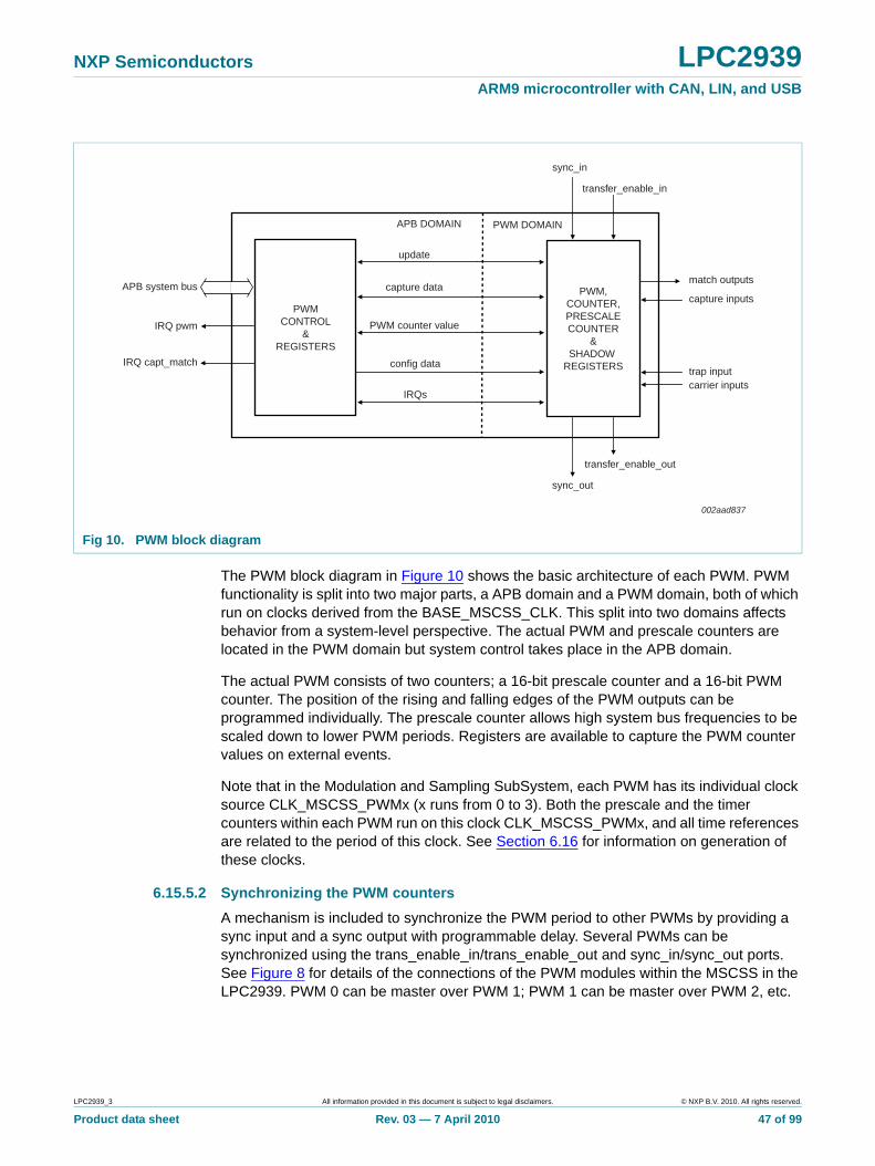
NXP Semiconductors LPC2939ARM9 microcontroller with CAN, LIN, and USB
The PWM block diagram in Figure 10 shows the basic architecture of each PWM. PWM functionality is split into two major parts, a APB domain and a PWM domain, both of which run on clocks derived from the BASE_MSCSS_CLK. This split into two domains affects behavior from a system-level perspective. The actual PWM and prescale counters are located in the PWM domain but system control takes place in the APB domain.
The actual PWM consists of two counters; a 16-bit prescale counter and a 16-bit PWM counter. The position of the rising and falling edges of the PWM outputs can be programmed individually. The prescale counter allows high system bus frequencies to be scaled down to lower PWM periods. Registers are available to capture the PWM counter values on external events.
Note that in the Modulation and Sampling SubSystem, each PWM has its individual clock source CLK_MSCSS_PWMx (x runs from 0 to 3). Both the prescale and the timer counters within each PWM run on this clock CLK_MSCSS_PWMx, and all time references are related to the period of this clock. See Section 6.16 for information on generation of these clocks.
6.15.5.2 Synchronizing the PWM counters
A mechanism is included to synchronize the PWM period to other PWMs by providing a sync input and a sync output with programmable delay. Several PWMs can be synchronized using the trans_enable_in/trans_enable_out and sync_in/sync_out ports. See Figure 8 for details of the connections of the PWM modules within the MSCSS in the LPC2939. PWM 0 can be master over PWM 1; PWM 1 can be master over PWM 2, etc.
Fig 10. PWM block diagram
002aad837
APB system bus
IRQ pwm
IRQ capt_match
PWMCONTROL
®ISTERS
update
capture data
PWM counter value
config data
IRQs
PWM,COUNTER,PRESCALECOUNTER
&SHADOW
REGISTERS
match outputs
capture inputs
trap inputcarrier inputs
sync_in
sync_out
transfer_enable_in
transfer_enable_out
APB DOMAIN PWM DOMAIN
LPC2939_3 All information provided in this document is subject to legal disclaimers. © NXP B.V. 2010. All rights reserved.
Product data sheet Rev. 03 — 7 April 2010 47 of 99
NXP Semiconductors LPC2939ARM9 microcontroller with CAN, LIN, and USB
6.15.5.3 Master and slave mode
A PWM module can provide synchronization signals to other modules (also called Master mode). The signal sync_out is a pulse of one clock cycle generated when the internal PWM counter (re)starts. The signal trans_enable_out is a pulse synchronous to sync_out, generated if a transfer from system registers to PWM shadow registers occurred when the PWM counter restarted. A delay may be inserted between the counter start and generation of trans_enable_out and sync_out.
A PWM module can use input signals trans_enable_in and sync_in to synchronize its internal PWM counter and the transfer of shadow registers (Slave mode).
6.15.5.4 Pin description
Each of the four PWM modules in the MSCSS has the following pins. These are combined with other functions on the port pins of the LPC2939. Table 24 shows the PWM0 to PWM3 pins.
6.15.5.5 Clock description
The PWM modules are clocked by CLK_MSCSS_PWMx (x = 0 to 3), see Section 6.7.2. Note that each PWM has its own CLK_MSCSS_PWMx branch clock for power management. The frequency of all these clocks is identical to CLK_MSCSS_APB since they are derived from the same base clock BASE_MSCSS_CLK.
Also note that unlike the timer modules in the Peripheral SubSystem, the actual timer counter registers of the PWM modules run at the same clock as the APB system interface CLK_MSCSS_APB. This clock is independent of the AHB system clock.
If a PWM module is not used its CLK_MSCSS_PWMx branch clock can be switched off.
6.15.6 Timers in the MSCSS
The two timers in the MSCSS are functionally identical to the timers in the peripheral subsystem, see Section 6.13.3. The features of the timers in the MSCSS are the same as the timers in the peripheral subsystem, but the capture inputs and match outputs are not available on the device pins. These signals are instead connected to the ADC and PWM modules as outlined in the description of the MSCSS, see Section 6.15.1.
See Section 6.13.3 for a functional description of the timers.
Table 24. PWM pins
Symbol Pin name Direction Description
PWMn CAP[0] PCAPn[0] IN PWM n capture input 0
PWMn CAP[1] PCAPn[1] IN PWM n capture input 1
PWMn CAP[2] PCAPn[2] IN PWM n capture input 2
PWMn MAT[0] PMATn[0] OUT PWM n match output 0
PWMn MAT[1] PMATn[1] OUT PWM n match output 1
PWMn MAT[2] PMATn[2] OUT PWM n match output 2
PWMn MAT[3] PMATn[3] OUT PWM n match output 3
PWMn MAT[4] PMATn[4] OUT PWM n match output 4
PWMn MAT[5] PMATn[5] OUT PWM n match output 5
PWMn TRAP TRAPn IN PWM n trap input
LPC2939_3 All information provided in this document is subject to legal disclaimers. © NXP B.V. 2010. All rights reserved.
Product data sheet Rev. 03 — 7 April 2010 48 of 99
NXP Semiconductors LPC2939ARM9 microcontroller with CAN, LIN, and USB
6.15.6.1 Pin description
MSCSS timer 0 has no external pins.
MSCSS timer 1 has a PAUSE pin available as external pin. The PAUSE pin is combined with other functions on the port pins of the LPC2939. Table 25 shows the MSCSS timer 1 external pin.
6.15.6.2 Clock description
The Timer modules in the MSCSS are clocked by CLK_MSCSS_MTMRx (x = 0 to 1), see Section 6.7.2. Note that each timer has its own CLK_MSCSS_MTMRx branch clock for power management. The frequency of all these clocks is identical to CLK_MSCSS_APB since they are derived from the same base clock BASE_MSCSS_CLK.
Note that, unlike the timer modules in the Peripheral SubSystem, the actual timer counter registers run at the same clock as the APB system interface CLK_MSCSS_APB. This clock is independent of the AHB system clock.
If a timer module is not used its CLK_MSCSS_MTMRx branch clock can be switched off.
6.15.7 Quadrature Encoder Interface (QEI)
A quadrature encoder, also known as a 2-channel incremental encoder, converts angular displacement into two pulse signals. By monitoring both the number of pulses and the relative phase of the two signals, the user can track the position, direction of rotation, and velocity. In addition, a third channel, or index signal, can be used to reset the position counter. The quadrature encoder interface decodes the digital pulses from a quadrature encoder wheel to integrate position over time and determine direction of rotation. In addition, the QEI can capture the velocity of the encoder wheel.
The QEI has the following features:
• Tracks encoder position
• Increments/ decrements depending on direction
• Programmable for 2 or 4 position counting
• Velocity capture using built-in timer
• Velocity compare function with less than interrupt
• Uses 32-bit registers for position and velocity
• Three position compare registers with interrupts
• Index counter for revolution counting
• Index compare register with interrupts
• Can combine index and position interrupts to produce an interrupt for whole and partial revolution displacement
• Digital filter with programmable delays for encoder input signals
• Can accept decoded signal inputs (clk and direction)
• Connected to APB
Table 25. MSCSS timer 1 pin
Symbol Direction Description
MSCSS PAUSE IN pause pin for MSCSS timer 1
LPC2939_3 All information provided in this document is subject to legal disclaimers. © NXP B.V. 2010. All rights reserved.
Product data sheet Rev. 03 — 7 April 2010 49 of 99
NXP Semiconductors LPC2939ARM9 microcontroller with CAN, LIN, and USB
6.15.7.1 Pin description
The QEI module in the MSCSS has the following pins. These are combined with other functions on the port pins of the LPC2939. Table 26 shows the QEI pins.
6.15.7.2 Clock description
The QEI module is clocked by CLK_MSCSS_QEI, see Section 6.7.2. The frequency of this clock is identical to CLK_MSCSS_APB since they are derived from the same base clock BASE_MSCSS_CLK.
If the QEI is not used its CLK_MSCSS_QEI branch clock can be switched off.
6.16 Power, Clock and Reset control SubSystem (PCRSS)
The Power, Clock and Reset Control Subsystem in the LPC2939 includes a Clock Generator Unit (CGU), a Reset Generator Unit (RGU), and a Power Management Unit (PMU).
Figure 11 provides an overview of the PCRSS. An AHB-to-DTL bridge controls the communication with the AHB system bus.
Table 26. QEI pins
Symbol Pin name Direction Description
QEI0 IDX IDX0 IN Index signal. Can be used to reset the position.
QEI0 PHA PHA0 IN Sensor signal. Corresponds to PHA in quadrature mode and to direction in clock/direction mode.
QEI0 PHB PHB0 IN Sensor signal. Corresponds to PHB in quadrature mode and to clock signal in clock/direction mode.
LPC2939_3 All information provided in this document is subject to legal disclaimers. © NXP B.V. 2010. All rights reserved.
Product data sheet Rev. 03 — 7 April 2010 50 of 99
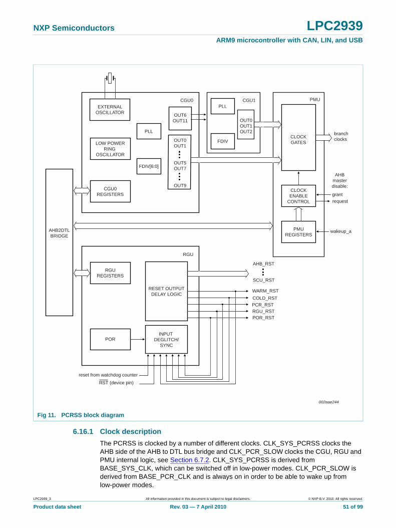
NXP Semiconductors LPC2939ARM9 microcontroller with CAN, LIN, and USB
6.16.1 Clock description
The PCRSS is clocked by a number of different clocks. CLK_SYS_PCRSS clocks the AHB side of the AHB to DTL bus bridge and CLK_PCR_SLOW clocks the CGU, RGU and PMU internal logic, see Section 6.7.2. CLK_SYS_PCRSS is derived from BASE_SYS_CLK, which can be switched off in low-power modes. CLK_PCR_SLOW is derived from BASE_PCR_CLK and is always on in order to be able to wake up from low-power modes.
Fig 11. PCRSS block diagram
002aae244
AHB2DTLBRIDGE
RESET OUTPUTDELAY LOGIC
INPUT DEGLITCH/
SYNC
branchclocks
grantrequest
wakeup_a
AHB_RST
SCU_RST
WARM_RST
COLD_RSTPCR_RSTRGU_RSTPOR_RST
RST (device pin)
reset from watchdog counter
EXTERNALOSCILLATOR
PMUREGISTERS
CLOCKENABLE
CONTROL
CLOCKGATESLOW POWER
RING OSCILLATOR
CGU0REGISTERS
RGUREGISTERS
POR
OUT0OUT1
OUT5OUT7
OUT9
OUT6OUT11 OUT0
OUT1OUT2PLL
FDIV[6:0]
PLL
FDIV
CGU0 CGU1 PMU
RGU
AHBmasterdisable:
LPC2939_3 All information provided in this document is subject to legal disclaimers. © NXP B.V. 2010. All rights reserved.
Product data sheet Rev. 03 — 7 April 2010 51 of 99
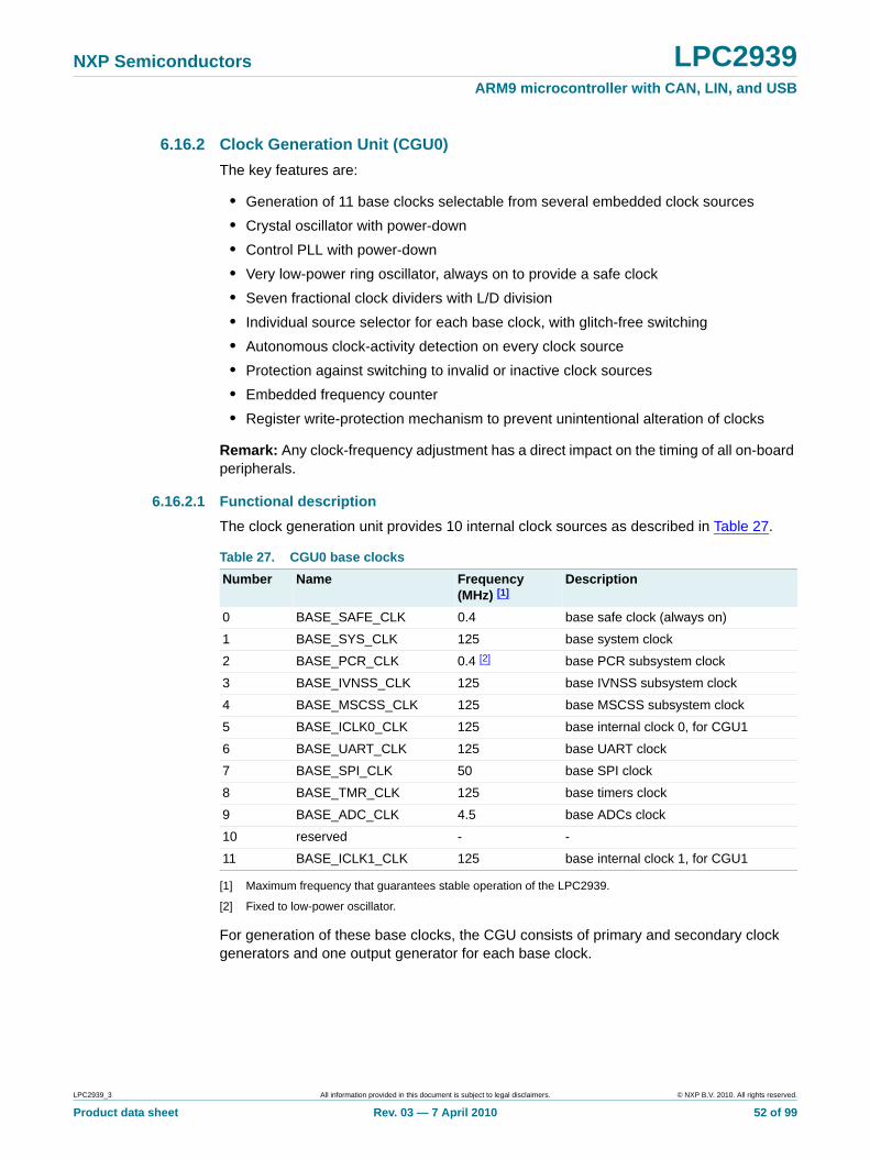
NXP Semiconductors LPC2939ARM9 microcontroller with CAN, LIN, and USB
6.16.2 Clock Generation Unit (CGU0)
The key features are:
• Generation of 11 base clocks selectable from several embedded clock sources
• Crystal oscillator with power-down
• Control PLL with power-down
• Very low-power ring oscillator, always on to provide a safe clock
• Seven fractional clock dividers with L/D division
• Individual source selector for each base clock, with glitch-free switching
• Autonomous clock-activity detection on every clock source
• Protection against switching to invalid or inactive clock sources
• Embedded frequency counter
• Register write-protection mechanism to prevent unintentional alteration of clocks
Remark: Any clock-frequency adjustment has a direct impact on the timing of all on-board peripherals.
6.16.2.1 Functional description
The clock generation unit provides 10 internal clock sources as described in Table 27.
[1] Maximum frequency that guarantees stable operation of the LPC2939.
[2] Fixed to low-power oscillator.
For generation of these base clocks, the CGU consists of primary and secondary clock generators and one output generator for each base clock.
Table 27. CGU0 base clocks
Number Name Frequency (MHz) [1]
Description
0 BASE_SAFE_CLK 0.4 base safe clock (always on)
1 BASE_SYS_CLK 125 base system clock
2 BASE_PCR_CLK 0.4 [2] base PCR subsystem clock
3 BASE_IVNSS_CLK 125 base IVNSS subsystem clock
4 BASE_MSCSS_CLK 125 base MSCSS subsystem clock
5 BASE_ICLK0_CLK 125 base internal clock 0, for CGU1
6 BASE_UART_CLK 125 base UART clock
7 BASE_SPI_CLK 50 base SPI clock
8 BASE_TMR_CLK 125 base timers clock
9 BASE_ADC_CLK 4.5 base ADCs clock
10 reserved - -
11 BASE_ICLK1_CLK 125 base internal clock 1, for CGU1
LPC2939_3 All information provided in this document is subject to legal disclaimers. © NXP B.V. 2010. All rights reserved.
Product data sheet Rev. 03 — 7 April 2010 52 of 99
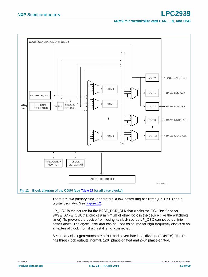
NXP Semiconductors LPC2939ARM9 microcontroller with CAN, LIN, and USB
There are two primary clock generators: a low-power ring oscillator (LP_OSC) and a crystal oscillator. See Figure 12.
LP_OSC is the source for the BASE_PCR_CLK that clocks the CGU itself and for BASE_SAFE_CLK that clocks a minimum of other logic in the device (like the watchdog timer). To prevent the device from losing its clock source LP_OSC cannot be put into power-down. The crystal oscillator can be used as source for high-frequency clocks or as an external clock input if a crystal is not connected.
Secondary clock generators are a PLL and seven fractional dividers (FDIV0:6). The PLL has three clock outputs: normal, 120 phase-shifted and 240 phase-shifted.
Fig 12. Block diagram of the CGU0 (see Table 27 for all base clocks)
400 kHz LP_OSC
PLL
FDIV0
EXTERNALOSCILLATOR
FDIV1
FDIV6
OUT 0
OUT 1
OUT 11
002aae147
clkoutclkout120clkout240
CLOCK GENERATION UNIT (CGU0)
FREQUENCYMONITOR
CLOCKDETECTION
AHB TO DTL BRIDGE
BASE_SYS_CLK
BASE_ICLK1_CLK
OUT 3 BASE_IVNSS_CLK
OUT 2 BASE_PCR_CLK
BASE_SAFE_CLK
LPC2939_3 All information provided in this document is subject to legal disclaimers. © NXP B.V. 2010. All rights reserved.
Product data sheet Rev. 03 — 7 April 2010 53 of 99
NXP Semiconductors LPC2939ARM9 microcontroller with CAN, LIN, and USB
Configuration of the CGU0: For every output generator generating the base clocks a choice can be made from the primary and secondary clock generators according to Figure 13.
Any output generator (except for BASE_SAFE_CLK and BASE_PCR_CLK) can be connected to either a fractional divider (FDIV0:6) or to one of the outputs of the PLL or to LP_OSC/crystal oscillator directly. BASE_SAFE_CLK and BASE_PCR_CLK can use only LP_OSC as source.
The fractional dividers can be connected to one of the outputs of the PLL or directly to LP_OSC/crystal Oscillator.
The PLL is connected to the crystal oscillator.
In this way every output generating the base clocks can be configured to get the required clock. Multiple output generators can be connected to the same primary or secondary clock source, and multiple secondary clock sources can be connected to the same PLL output or primary clock source.
Invalid selections/programming - connecting the PLL to an FDIV or to one of the PLL outputs itself for example - will be blocked by hardware. The control register will not be written, the previous value will be kept, although all other fields will be written with new data. This prevents clocks being blocked by incorrect programming.
Default Clock Sources: Every secondary clock generator or output generator is connected to LP_OSC at reset. In this way the device runs at a low frequency after reset. It is recommended to switch BASE_SYS_CLK to a high-frequency clock generator as (one of) the first step(s) in the boot code after verifying that the high-frequency clock generator is running.
Clock Activity Detection: Clocks that are inactive are automatically regarded as invalid, and values of ‘CLK_SEL’ that would select those clocks are masked and not written to the control registers. This is accomplished by adding a clock detector to every clock
Fig 13. Structure of the clock generation scheme
LP_OSC
PLL
FDIV0:6
EXTERNALOSCILLATOR
002aad834
clkoutclkout120clkout240
OUTPUTCONTROL
clockoutputs
LPC2939_3 All information provided in this document is subject to legal disclaimers. © NXP B.V. 2010. All rights reserved.
Product data sheet Rev. 03 — 7 April 2010 54 of 99
NXP Semiconductors LPC2939ARM9 microcontroller with CAN, LIN, and USB
generator. The RDET register keeps track of which clocks are active and inactive, and the appropriate ‘CLK_SEL’ values are masked and unmasked accordingly. Each clock detector can also generate interrupts at clock activation and deactivation so that the system can be notified of a change in internal clock status.
Clock detection is done using a counter running at the BASE_PCR_CLK frequency. If no positive clock edge occurs before the counter has 32 cycles of BASE_PCR_CLK the clock is assumed to be inactive. As BASE_PCR_CLK is slower than any of the clocks to be detected, normally only one BASE_PCR_CLK cycle is needed to detect activity. After reset all clocks are assumed to be ‘non-present’, so the RDET status register will be correct only after 32 BASE_PCR_CLK cycles.
Note that this mechanism cannot protect against a currently-selected clock going from active to inactive state. Therefore an inactive clock may still be sent to the system under special circumstances, although an interrupt can still be generated to notify the system.
Glitch-Free Switching: Provisions are included in the CGU to allow clocks to be switched glitch-free, both at the output generator stage and also at secondary source generators.
In the case of the PLL the clock will be stopped and held LOW for long enough to allow the PLL to stabilize and lock before being re-enabled. For all non-PLL Generators the switch will occur as quickly as possible, although there will always be a period when the clock is held LOW due to synchronization requirements.
If the current clock is HIGH and does not go LOW within 32 cycles of BASE_PCR_CLK it is assumed to be inactive and is asynchronously forced LOW. This prevents deadlocks on the interface.
6.16.2.2 PLL functional description
A block diagram of the PLL is shown in Figure 14. The input clock is fed directly to the analog section. This block compares the phase and frequency of the inputs and generates the main clock2. These clocks are either divided by 2 P by the programmable post divider to create the output clock, or sent directly to the output. The main output clock is then divided by M by the programmable feedback divider to generate the feedback clock. The output signal of the analog section is also monitored by the lock detector to signal when the PLL has locked onto the input clock.
2. Generation of the main clock is restricted by the frequency range of the PLL clock input. See Table 36, Dynamic characteristics.
LPC2939_3 All information provided in this document is subject to legal disclaimers. © NXP B.V. 2010. All rights reserved.
Product data sheet Rev. 03 — 7 April 2010 55 of 99
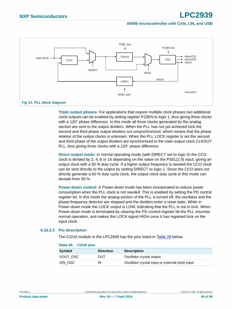
NXP Semiconductors LPC2939ARM9 microcontroller with CAN, LIN, and USB
Triple output phases: For applications that require multiple clock phases two additional clock outputs can be enabled by setting register P23EN to logic 1, thus giving three clocks with a 120 phase difference. In this mode all three clocks generated by the analog section are sent to the output dividers. When the PLL has not yet achieved lock the second and third phase output dividers run unsynchronized, which means that the phase relation of the output clocks is unknown. When the PLL LOCK register is set the second and third phase of the output dividers are synchronized to the main output clock CLKOUT PLL, thus giving three clocks with a 120 phase difference.
Direct output mode: In normal operating mode (with DIRECT set to logic 0) the CCO clock is divided by 2, 4, 8 or 16 depending on the value on the PSEL[1:0] input, giving an output clock with a 50 % duty cycle. If a higher output frequency is needed the CCO clock can be sent directly to the output by setting DIRECT to logic 1. Since the CCO does not directly generate a 50 % duty cycle clock, the output clock duty cycle in this mode can deviate from 50 %.
Power-down control: A Power-down mode has been incorporated to reduce power consumption when the PLL clock is not needed. This is enabled by setting the PD control register bit. In this mode the analog section of the PLL is turned off, the oscillator and the phase-frequency detector are stopped and the dividers enter a reset state. While in Power-down mode the LOCK output is LOW, indicating that the PLL is not in lock. When Power-down mode is terminated by clearing the PD control-register bit the PLL resumes normal operation, and makes the LOCK signal HIGH once it has regained lock on the input clock.
6.16.2.3 Pin description
The CGU0 module in the LPC2939 has the pins listed in Table 28 below.
Fig 14. PLL block diagram
CCO/ 2PDIV
P23
/ MDIV
002aad833
bypassdirect
clkout120clkout240clkout
clkout
input clock
PSEL bitsP23EN bit
MSEL bits
Table 28. CGU0 pins
Symbol Direction Description
XOUT_OSC OUT Oscillator crystal output
XIN_OSC IN Oscillator crystal input or external clock input
LPC2939_3 All information provided in this document is subject to legal disclaimers. © NXP B.V. 2010. All rights reserved.
Product data sheet Rev. 03 — 7 April 2010 56 of 99
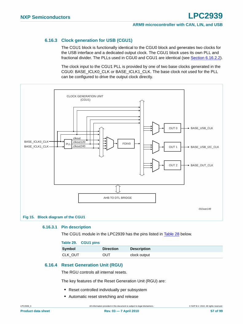
NXP Semiconductors LPC2939ARM9 microcontroller with CAN, LIN, and USB
6.16.3 Clock generation for USB (CGU1)
The CGU1 block is functionally identical to the CGU0 block and generates two clocks for the USB interface and a dedicated output clock. The CGU1 block uses its own PLL and fractional divider. The PLLs used in CGU0 and CGU1 are identical (see Section 6.16.2.2).
The clock input to the CGU1 PLL is provided by one of two base clocks generated in the CGU0: BASE_ICLK0_CLK or BASE_ICLK1_CLK. The base clock not used for the PLL can be configured to drive the output clock directly.
6.16.3.1 Pin description
The CGU1 module in the LPC2939 has the pins listed in Table 28 below.
6.16.4 Reset Generation Unit (RGU)
The RGU controls all internal resets.
The key features of the Reset Generation Unit (RGU) are:
• Reset controlled individually per subsystem
• Automatic reset stretching and release
Fig 15. Block diagram of the CGU1
PLL FDIV0
OUT 0
OUT 2
002aae148
clkoutclkout120clkout240
CLOCK GENERATION UNIT (CGU1)
AHB TO DTL BRIDGE
BASE_USB_CLK
BASE_OUT_CLK
OUT 1 BASE_USB_I2C_CLKBASE_ICLK1_CLK
BASE_ICLK0_CLK
Table 29. CGU1 pins
Symbol Direction Description
CLK_OUT OUT clock output
LPC2939_3 All information provided in this document is subject to legal disclaimers. © NXP B.V. 2010. All rights reserved.
Product data sheet Rev. 03 — 7 April 2010 57 of 99
NXP Semiconductors LPC2939ARM9 microcontroller with CAN, LIN, and USB
• Monitor function to trace resets back to source
• Register write-protection mechanism to prevent unintentional resets
6.16.4.1 Functional description
Each reset output is defined as a combination of reset input sources including the external reset input pins and internal power-on reset, see Table 30. The first five resets listed in this table form a sort of cascade to provide the multiple levels of impact that a reset may have. The combined input sources are logically OR-ed together so that activating any of the listed reset sources causes the output to go active.
6.16.4.2 Pin description
The RGU module in the LPC2939 has the following pins. Table 31 shows the RGU pins.
Table 30. Reset output configuration
Reset output Reset source Parts of the device reset when activated
POR_RST power-on reset module LP_OSC; source for RGU_RST
RGU_RST POR_RST, RST pin RGU internal; source for PCR_RST
PCR_RST RGU_RST, WATCHDOG PCR internal; source for COLD_RST
COLD_RST PCR_RST parts with COLD_RST as reset source below
WARM_RST COLD_RST parts with WARM_RST as reset source below
SCU_RST COLD_RST SCU
CFID_RST COLD_RST CFID
FMC_RST COLD_RST embedded Flash-Memory Controller (FMC)
EMC_RST COLD_RST embedded SRAM-Memory Controller
SMC_RST COLD_RST external Static-Memory Controller (SMC)
GESS_A2V_RST WARM_RST GeSS AHB-to-APB bridge
PESS_A2V_RST WARM_RST PeSS AHB-to-APB bridge
GPIO_RST WARM_RST all GPIO modules
UART_RST WARM_RST all UART modules
TMR_RST WARM_RST all Timer modules in PESS
SPI_RST WARM_RST all SPI modules
IVNSS_A2V_RST WARM_RST IVNSS AHB-to-APB bridge
IVNSS_CAN_RST WARM_RST all CAN modules including Acceptance filter
IVNSS_LIN_RST WARM_RST all LIN modules
MSCSS_A2V_RST WARM_RST MSCSS AHB to APB bridge
MSCSS_PWM_RST WARM_RST all PWM modules
MSCSS_ADC_RST WARM_RST all ADC modules
MSCSS_TMR_RST WARM_RST all Timer modules in MSCSS
I2C_RST WARM_RST all I2C modules
QEI_RST WARM_RST Quadrature encoder
DMA_RST WARM_RST GPDMA controller
USB_RST WARM_RST USB controller
VIC_RST WARM_RST Vectored Interrupt Controller (VIC)
AHB_RST WARM_RST CPU and AHB Bus infrastructure
LPC2939_3 All information provided in this document is subject to legal disclaimers. © NXP B.V. 2010. All rights reserved.
Product data sheet Rev. 03 — 7 April 2010 58 of 99
NXP Semiconductors LPC2939ARM9 microcontroller with CAN, LIN, and USB
6.16.5 Power Management Unit (PMU)
This module enables software to actively control the system’s power consumption by disabling clocks not required in a particular operating mode.
Using the base clocks from the CGU as input, the PMU generates branch clocks to the rest of the LPC2939. Output clocks branched from the same base clock are phase- and frequency-related. These branch clocks can be individually controlled by software programming.
The key features are:
• Individual clock control for all LPC2939 sub-modules
• Activates sleeping clocks when a wake-up event is detected
• Clocks can be individually disabled by software
• Supports AHB master-disable protocol when AUTO mode is set
• Disables wake-up of enabled clocks when Power-down mode is set
• Activates wake-up of enabled clocks when a wake-up event is received
• Status register is available to indicate if an input base clock can be safely switched off (i.e. all branch clocks are disabled)
6.16.5.1 Functional description
The PMU controls all internal clocks coming out of the CGU0 for power-mode management. With some exceptions, each branch clock can be switched on or off individually under control of software register bits located in its individual configuration register. Some branch clocks controlling vital parts of the device operate in a fixed mode. Table 32 shows which mode control bits are supported by each branch clock.
By programming the configuration register the user can control which clocks are switched on or off, and which clocks are switched off when entering Power-down mode.
Note that the standby-wait-for-interrupt instructions of the ARM968E-S processor (putting the ARM CPU into a low-power state) are not supported. Instead putting the ARM CPU into power-down should be controlled by disabling the branch clock for the CPU.
Remark: For any disabled branch clocks to be re-activated their corresponding base clocks must be running (controlled by the CGU0).
Table 32 shows the relation between branch and base clocks, see also Section 6.7.1. Every branch clock is related to one particular base clock: it is not possible to switch the source of a branch clock in the PMU.
Table 31. RGU pins
Symbol Direction Description
RST IN external reset input, active LOW; pulled up internally
LPC2939_3 All information provided in this document is subject to legal disclaimers. © NXP B.V. 2010. All rights reserved.
Product data sheet Rev. 03 — 7 April 2010 59 of 99
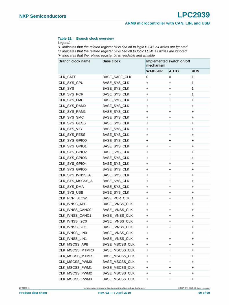
NXP Semiconductors LPC2939ARM9 microcontroller with CAN, LIN, and USB
Table 32. Branch clock overviewLegend:‘1’ Indicates that the related register bit is tied off to logic HIGH, all writes are ignored‘0’ Indicates that the related register bit is tied off to logic LOW, all writes are ignored‘+’ Indicates that the related register bit is readable and writable
Branch clock name Base clock Implemented switch on/off mechanism
WAKE-UP AUTO RUN
CLK_SAFE BASE_SAFE_CLK 0 0 1
CLK_SYS_CPU BASE_SYS_CLK + + 1
CLK_SYS BASE_SYS_CLK + + 1
CLK_SYS_PCR BASE_SYS_CLK + + 1
CLK_SYS_FMC BASE_SYS_CLK + + +
CLK_SYS_RAM0 BASE_SYS_CLK + + +
CLK_SYS_RAM1 BASE_SYS_CLK + + +
CLK_SYS_SMC BASE_SYS_CLK + + +
CLK_SYS_GESS BASE_SYS_CLK + + +
CLK_SYS_VIC BASE_SYS_CLK + + +
CLK_SYS_PESS BASE_SYS_CLK + + +
CLK_SYS_GPIO0 BASE_SYS_CLK + + +
CLK_SYS_GPIO1 BASE_SYS_CLK + + +
CLK_SYS_GPIO2 BASE_SYS_CLK + + +
CLK_SYS_GPIO3 BASE_SYS_CLK + + +
CLK_SYS_GPIO4 BASE_SYS_CLK + + +
CLK_SYS_GPIO5 BASE_SYS_CLK + + +
CLK_SYS_IVNSS_A BASE_SYS_CLK + + +
CLK_SYS_MSCSS_A BASE_SYS_CLK + + +
CLK_SYS_DMA BASE_SYS_CLK + + +
CLK_SYS_USB BASE_SYS_CLK + + +
CLK_PCR_SLOW BASE_PCR_CLK + + 1
CLK_IVNSS_APB BASE_IVNSS_CLK + + +
CLK_IVNSS_CANC0 BASE_IVNSS_CLK + + +
CLK_IVNSS_CANC1 BASE_IVNSS_CLK + + +
CLK_IVNSS_I2C0 BASE_IVNSS_CLK + + +
CLK_IVNSS_I2C1 BASE_IVNSS_CLK + + +
CLK_IVNSS_LIN0 BASE_IVNSS_CLK + + +
CLK_IVNSS_LIN1 BASE_IVNSS_CLK + + +
CLK_MSCSS_APB BASE_MSCSS_CLK + + +
CLK_MSCSS_MTMR0 BASE_MSCSS_CLK + + +
CLK_MSCSS_MTMR1 BASE_MSCSS_CLK + + +
CLK_MSCSS_PWM0 BASE_MSCSS_CLK + + +
CLK_MSCSS_PWM1 BASE_MSCSS_CLK + + +
CLK_MSCSS_PWM2 BASE_MSCSS_CLK + + +
CLK_MSCSS_PWM3 BASE_MSCSS_CLK + + +
LPC2939_3 All information provided in this document is subject to legal disclaimers. © NXP B.V. 2010. All rights reserved.
Product data sheet Rev. 03 — 7 April 2010 60 of 99
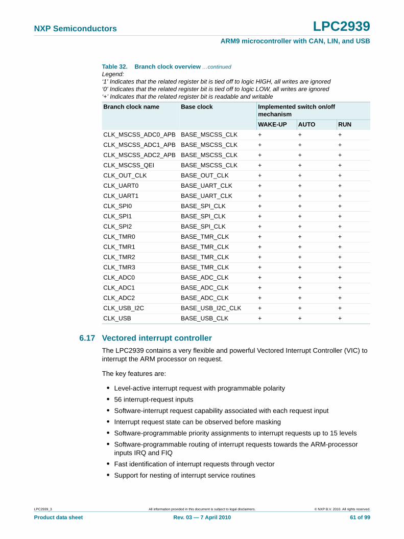
NXP Semiconductors LPC2939ARM9 microcontroller with CAN, LIN, and USB
6.17 Vectored interrupt controller
The LPC2939 contains a very flexible and powerful Vectored Interrupt Controller (VIC) to interrupt the ARM processor on request.
The key features are:
• Level-active interrupt request with programmable polarity
• 56 interrupt-request inputs
• Software-interrupt request capability associated with each request input
• Interrupt request state can be observed before masking
• Software-programmable priority assignments to interrupt requests up to 15 levels
• Software-programmable routing of interrupt requests towards the ARM-processor inputs IRQ and FIQ
• Fast identification of interrupt requests through vector
• Support for nesting of interrupt service routines
CLK_MSCSS_ADC0_APB BASE_MSCSS_CLK + + +
CLK_MSCSS_ADC1_APB BASE_MSCSS_CLK + + +
CLK_MSCSS_ADC2_APB BASE_MSCSS_CLK + + +
CLK_MSCSS_QEI BASE_MSCSS_CLK + + +
CLK_OUT_CLK BASE_OUT_CLK + + +
CLK_UART0 BASE_UART_CLK + + +
CLK_UART1 BASE_UART_CLK + + +
CLK_SPI0 BASE_SPI_CLK + + +
CLK_SPI1 BASE_SPI_CLK + + +
CLK_SPI2 BASE_SPI_CLK + + +
CLK_TMR0 BASE_TMR_CLK + + +
CLK_TMR1 BASE_TMR_CLK + + +
CLK_TMR2 BASE_TMR_CLK + + +
CLK_TMR3 BASE_TMR_CLK + + +
CLK_ADC0 BASE_ADC_CLK + + +
CLK_ADC1 BASE_ADC_CLK + + +
CLK_ADC2 BASE_ADC_CLK + + +
CLK_USB_I2C BASE_USB_I2C_CLK + + +
CLK_USB BASE_USB_CLK + + +
Table 32. Branch clock overview …continuedLegend:‘1’ Indicates that the related register bit is tied off to logic HIGH, all writes are ignored‘0’ Indicates that the related register bit is tied off to logic LOW, all writes are ignored‘+’ Indicates that the related register bit is readable and writable
Branch clock name Base clock Implemented switch on/off mechanism
WAKE-UP AUTO RUN
LPC2939_3 All information provided in this document is subject to legal disclaimers. © NXP B.V. 2010. All rights reserved.
Product data sheet Rev. 03 — 7 April 2010 61 of 99
NXP Semiconductors LPC2939ARM9 microcontroller with CAN, LIN, and USB
6.17.1 Functional description
The Vectored Interrupt Controller routes incoming interrupt requests to the ARM processor. The interrupt target is configured for each interrupt request input of the VIC. The targets are defined as follows:
• Target 0 is ARM processor FIQ (fast interrupt service)
• Target 1 is ARM processor IRQ (standard interrupt service)
Interrupt-request masking is performed individually per interrupt target by comparing the priority level assigned to a specific interrupt request with a target-specific priority threshold. The priority levels are defined as follows:
• Priority level 0 corresponds to ‘masked’ (i.e. interrupt requests with priority 0 never lead to an interrupt)
• Priority 1 corresponds to the lowest priority
• Priority 15 corresponds to the highest priority
Software interrupt support is provided and can be supplied for:
• Testing RTOS (Real-Time Operating System) interrupt handling without using device-specific interrupt service routines
• Software emulation of an interrupt-requesting device, including interrupts
6.17.2 Clock description
The VIC is clocked by CLK_SYS_VIC, see Section 6.7.2.
LPC2939_3 All information provided in this document is subject to legal disclaimers. © NXP B.V. 2010. All rights reserved.
Product data sheet Rev. 03 — 7 April 2010 62 of 99
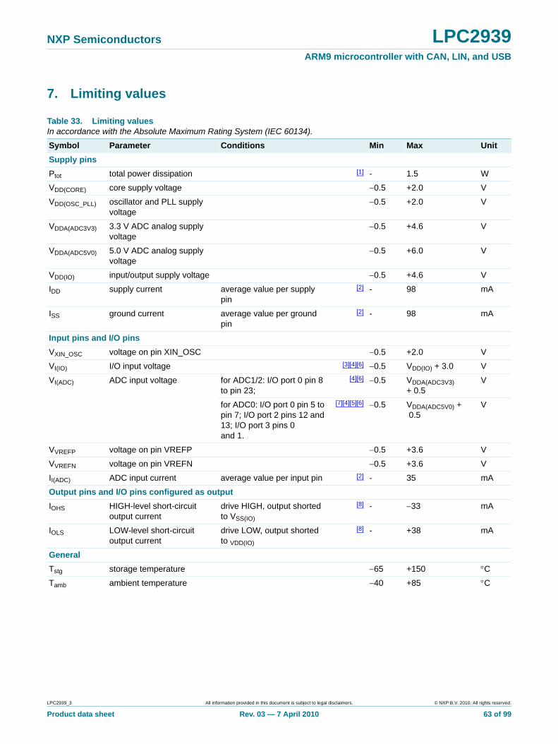
NXP Semiconductors LPC2939ARM9 microcontroller with CAN, LIN, and USB
7. Limiting values
Table 33. Limiting valuesIn accordance with the Absolute Maximum Rating System (IEC 60134).
Symbol Parameter Conditions Min Max Unit
Supply pins
Ptot total power dissipation [1] - 1.5 W
VDD(CORE) core supply voltage 0.5 +2.0 V
VDD(OSC_PLL) oscillator and PLL supply voltage
0.5 +2.0 V
VDDA(ADC3V3) 3.3 V ADC analog supply voltage
0.5 +4.6 V
VDDA(ADC5V0) 5.0 V ADC analog supply voltage
0.5 +6.0 V
VDD(IO) input/output supply voltage 0.5 +4.6 V
IDD supply current average value per supply pin
[2] - 98 mA
ISS ground current average value per ground pin
[2] - 98 mA
Input pins and I/O pins
VXIN_OSC voltage on pin XIN_OSC 0.5 +2.0 V
VI(IO) I/O input voltage [3][4][6] 0.5 VDD(IO) + 3.0 V
VI(ADC) ADC input voltage for ADC1/2: I/O port 0 pin 8 to pin 23;
[4][6] 0.5 VDDA(ADC3V3)
+ 0.5V
for ADC0: I/O port 0 pin 5 to pin 7; I/O port 2 pins 12 and 13; I/O port 3 pins 0and 1.
[7][4][5][6] 0.5 VDDA(ADC5V0) +0.5
V
VVREFP voltage on pin VREFP 0.5 +3.6 V
VVREFN voltage on pin VREFN 0.5 +3.6 V
II(ADC) ADC input current average value per input pin [2] - 35 mA
Output pins and I/O pins configured as output
IOHS HIGH-level short-circuit output current
drive HIGH, output shorted to VSS(IO)
[8] - 33 mA
IOLS LOW-level short-circuit output current
drive LOW, output shorted to VDD(IO)
[8] - +38 mA
General
Tstg storage temperature 65 +150 C
Tamb ambient temperature 40 +85 C
LPC2939_3 All information provided in this document is subject to legal disclaimers. © NXP B.V. 2010. All rights reserved.
Product data sheet Rev. 03 — 7 April 2010 63 of 99
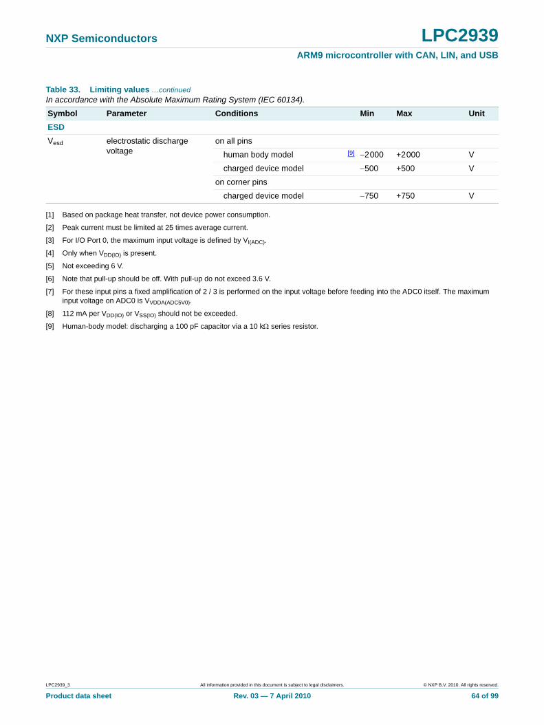
NXP Semiconductors LPC2939ARM9 microcontroller with CAN, LIN, and USB
[1] Based on package heat transfer, not device power consumption.
[2] Peak current must be limited at 25 times average current.
[3] For I/O Port 0, the maximum input voltage is defined by VI(ADC).
[4] Only when VDD(IO) is present.
[5] Not exceeding 6 V.
[6] Note that pull-up should be off. With pull-up do not exceed 3.6 V.
[7] For these input pins a fixed amplification of 2 / 3 is performed on the input voltage before feeding into the ADC0 itself. The maximum input voltage on ADC0 is VVDDA(ADC5V0).
[8] 112 mA per VDD(IO) or VSS(IO) should not be exceeded.
[9] Human-body model: discharging a 100 pF capacitor via a 10 k series resistor.
ESD
Vesd electrostatic discharge voltage
on all pins
human body model [9] 2000 +2000 V
charged device model 500 +500 V
on corner pins
charged device model 750 +750 V
Table 33. Limiting values …continuedIn accordance with the Absolute Maximum Rating System (IEC 60134).
Symbol Parameter Conditions Min Max Unit
LPC2939_3 All information provided in this document is subject to legal disclaimers. © NXP B.V. 2010. All rights reserved.
Product data sheet Rev. 03 — 7 April 2010 64 of 99
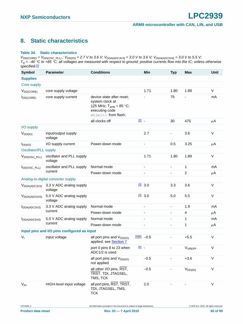
NXP Semiconductors LPC2939ARM9 microcontroller with CAN, LIN, and USB
8. Static characteristics
Table 34. Static characteristicsVDD(CORE) = VDD(OSC_PLL) ; VDD(IO) = 2.7 V to 3.6 V; VDDA(ADC3V3) = 3.0 V to 3.6 V; VDDA(ADC5V0) = 3.0 V to 5.5 V; Tvj = 40 C to +85 C; all voltages are measured with respect to ground; positive currents flow into the IC; unless otherwise specified.[1]
Symbol Parameter Conditions Min Typ Max Unit
Supplies
Core supply
VDD(CORE) core supply voltage 1.71 1.80 1.89 V
IDD(CORE) core supply current device state after reset; system clock at 125 MHz; Tamb = 85 C; executing code while(1){} from flash;
- 75 - mA
all clocks off [2] - 30 475 A
I/O supply
VDD(IO) input/output supply voltage
2.7 - 3.6 V
IDD(IO) I/O supply current Power-down mode - 0.5 3.25 A
Oscillator/PLL supply
VDD(OSC_PLL) oscillator and PLL supply voltage
1.71 1.80 1.89 V
IDD(OSC_PLL) oscillator and PLL supply current
Normal mode - - 1 mA
Power-down mode - - 2 A
Analog-to-digital converter supply
VDDA(ADC3V3) 3.3 V ADC analog supply voltage
[3] 3.0 3.3 3.6 V
VDDA(ADC5V0) 5.0 V ADC analog supply voltage
[4] 3.0 5.0 5.5 V
IDDA(ADC3V3) 3.3 V ADC analog supply current
Normal mode - - 1.9 mA
Power-down mode - - 4 A
IDDA(ADC5V0) 5.0 V ADC analog supply current
Normal mode - - 1 mA
Power-down mode - - 1 A
Input pins and I/O pins configured as input
VI input voltage all port pins and VDD(IO) applied; see Section 7
[5][6] 0.5 - +5.5 V
port 0 pins 8 to 23 when ADC1/2 is used
[6] - - VVREFP V
all port pins and VDD(IO) not applied
0.5 - +3.6 V
all other I/O pins, RST, TRST, TDI, JTAGSEL, TMS, TCK
0.5 - VDD(IO) V
VIH HIGH-level input voltage all port pins, RST, TRST, TDI, JTAGSEL, TMS, TCK
2.0 - - V
LPC2939_3 All information provided in this document is subject to legal disclaimers. © NXP B.V. 2010. All rights reserved.
Product data sheet Rev. 03 — 7 April 2010 65 of 99
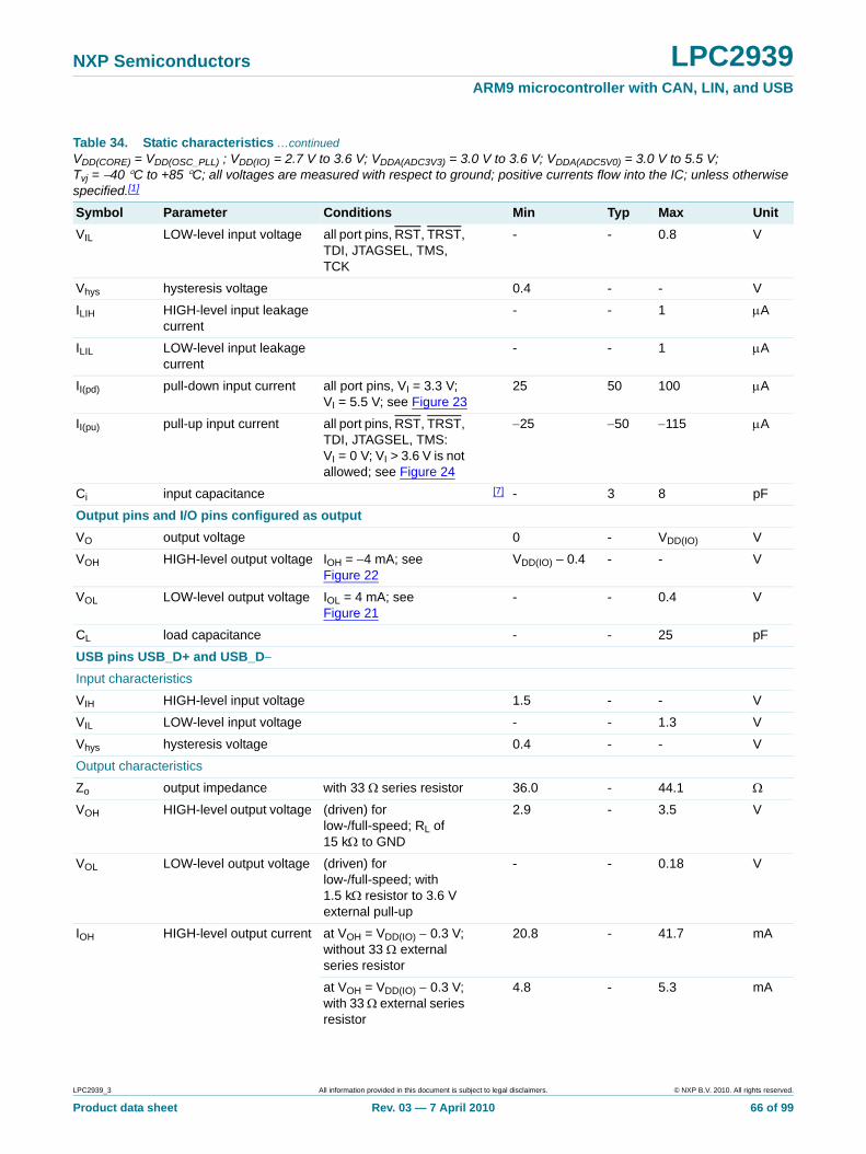
NXP Semiconductors LPC2939ARM9 microcontroller with CAN, LIN, and USB
VIL LOW-level input voltage all port pins, RST, TRST, TDI, JTAGSEL, TMS, TCK
- - 0.8 V
Vhys hysteresis voltage 0.4 - - V
ILIH HIGH-level input leakage current
- - 1 A
ILIL LOW-level input leakage current
- - 1 A
II(pd) pull-down input current all port pins, VI = 3.3 V; VI = 5.5 V; see Figure 23
25 50 100 A
II(pu) pull-up input current all port pins, RST, TRST, TDI, JTAGSEL, TMS: VI = 0 V; VI > 3.6 V is not allowed; see Figure 24
25 50 115 A
Ci input capacitance [7] - 3 8 pF
Output pins and I/O pins configured as output
VO output voltage 0 - VDD(IO) V
VOH HIGH-level output voltage IOH = 4 mA; see Figure 22
VDD(IO) – 0.4 - - V
VOL LOW-level output voltage IOL = 4 mA; see Figure 21
- - 0.4 V
CL load capacitance - - 25 pF
USB pins USB_D+ and USB_D
Input characteristics
VIH HIGH-level input voltage 1.5 - - V
VIL LOW-level input voltage - - 1.3 V
Vhys hysteresis voltage 0.4 - - V
Output characteristics
Zo output impedance with 33 series resistor 36.0 - 44.1
VOH HIGH-level output voltage (driven) for low-/full-speed; RL of 15 k to GND
2.9 - 3.5 V
VOL LOW-level output voltage (driven) for low-/full-speed; with 1.5 k resistor to 3.6 V external pull-up
- - 0.18 V
IOH HIGH-level output current at VOH = VDD(IO) 0.3 V; without 33 external series resistor
20.8 - 41.7 mA
at VOH = VDD(IO) 0.3 V; with 33 external series resistor
4.8 - 5.3 mA
Table 34. Static characteristics …continuedVDD(CORE) = VDD(OSC_PLL) ; VDD(IO) = 2.7 V to 3.6 V; VDDA(ADC3V3) = 3.0 V to 3.6 V; VDDA(ADC5V0) = 3.0 V to 5.5 V; Tvj = 40 C to +85 C; all voltages are measured with respect to ground; positive currents flow into the IC; unless otherwise specified.[1]
Symbol Parameter Conditions Min Typ Max Unit
LPC2939_3 All information provided in this document is subject to legal disclaimers. © NXP B.V. 2010. All rights reserved.
Product data sheet Rev. 03 — 7 April 2010 66 of 99
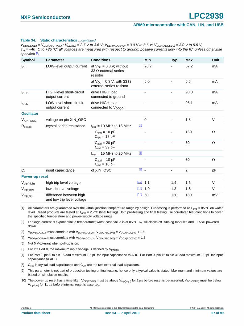
NXP Semiconductors LPC2939ARM9 microcontroller with CAN, LIN, and USB
[1] All parameters are guaranteed over the virtual junction temperature range by design. Pre-testing is performed at Tamb = 85 C on wafer level. Cased products are tested at Tamb = 25 C (final testing). Both pre-testing and final testing use correlated test conditions to cover the specified temperature and power-supply voltage range.
[2] Leakage current is exponential to temperature; worst-case value is at 85 C Tvj. All clocks off. Analog modules and FLASH powered down.
[3] VDDA(ADC3V3) must correlate with VDDA(ADC5V0): VDDA(ADC3V3) = VDDA(ADC5V0) / 1.5.
[4] VDDA(ADC5V0) must correlate with VDDA(ADC3V3): VDDA(ADC5V0) = VDDA(ADC3V3) 1.5.
[5] Not 5 V-tolerant when pull-up is on.
[6] For I/O Port 0, the maximum input voltage is defined by VI(ADC).
[7] For Port 0, pin 0 to pin 15 add maximum 1.5 pF for input capacitance to ADC. For Port 0, pin 16 to pin 31 add maximum 1.0 pF for input capacitance to ADC.
[8] Cxtal is crystal load capacitance and Cext are the two external load capacitors.
[9] This parameter is not part of production testing or final testing, hence only a typical value is stated. Maximum and minimum values are based on simulation results.
[10] The power-up reset has a time filter: VDD(CORE) must be above Vtrip(high) for 2 s before reset is de-asserted; VDD(CORE) must be below Vtrip(low) for 11 s before internal reset is asserted.
IOL LOW-level output current at VOL = 0.3 V; without 33 external series resistor
26.7 - 57.2 mA
at VOL = 0.3 V; with 33 external series resistor
5.0 - 5.5 mA
IOHS HIGH-level short-circuit output current
drive HIGH; pad connected to ground
- - 90.0 mA
IOLS LOW-level short-circuit output current
drive HIGH; pad connected to VDD(IO)
- - 95.1 mA
Oscillator
VXIN_OSC voltage on pin XIN_OSC 0 - 1.8 V
Rs(xtal) crystal series resistance fosc = 10 MHz to 15 MHz [8]
Cxtal = 10 pF; Cext = 18 pF
- - 160
Cxtal = 20 pF; Cext = 39 pF
- - 60
fosc = 15 MHz to 20 MHz [8]
Cxtal = 10 pF; Cext = 18 pF
- - 80
Ci input capacitance of XIN_OSC [9] - - 2 pF
Power-up reset
Vtrip(high) high trip level voltage [10] 1.1 1.4 1.6 V
Vtrip(low) low trip level voltage [10] 1.0 1.3 1.5 V
Vtrip(dif) difference between high and low trip level voltage
[10] 50 120 180 mV
Table 34. Static characteristics …continuedVDD(CORE) = VDD(OSC_PLL) ; VDD(IO) = 2.7 V to 3.6 V; VDDA(ADC3V3) = 3.0 V to 3.6 V; VDDA(ADC5V0) = 3.0 V to 5.5 V; Tvj = 40 C to +85 C; all voltages are measured with respect to ground; positive currents flow into the IC; unless otherwise specified.[1]
Symbol Parameter Conditions Min Typ Max Unit
LPC2939_3 All information provided in this document is subject to legal disclaimers. © NXP B.V. 2010. All rights reserved.
Product data sheet Rev. 03 — 7 April 2010 67 of 99
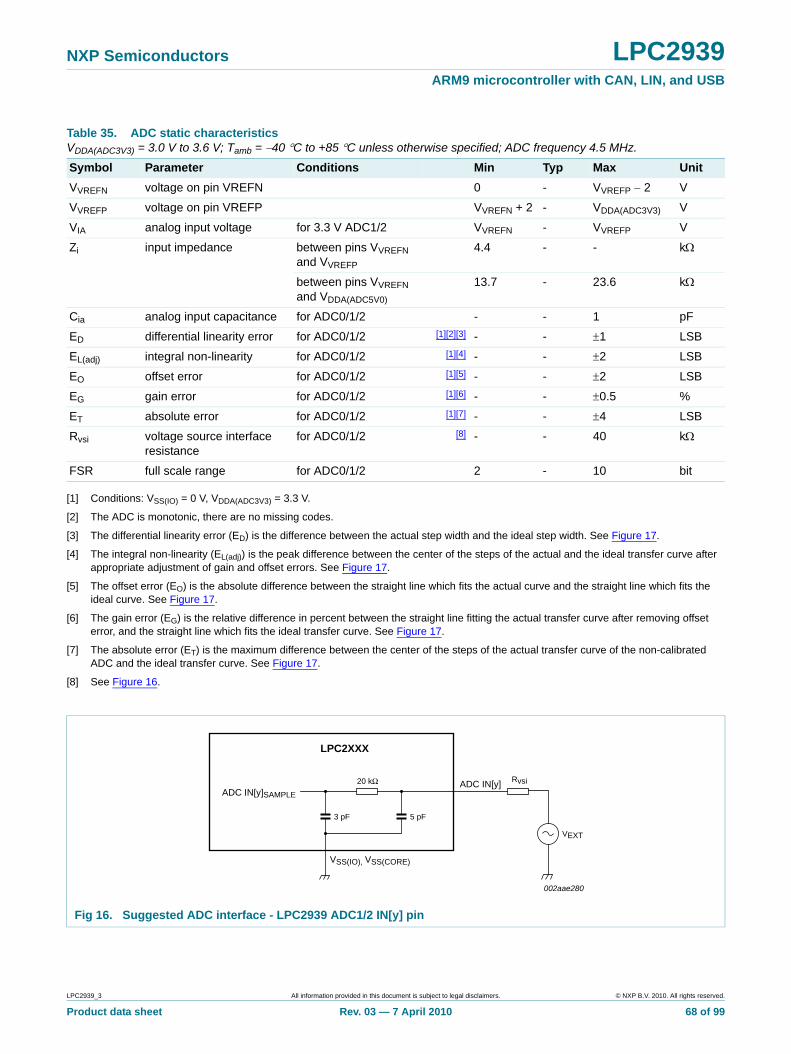
NXP Semiconductors LPC2939ARM9 microcontroller with CAN, LIN, and USB
[1] Conditions: VSS(IO) = 0 V, VDDA(ADC3V3) = 3.3 V.
[2] The ADC is monotonic, there are no missing codes.
[3] The differential linearity error (ED) is the difference between the actual step width and the ideal step width. See Figure 17.
[4] The integral non-linearity (EL(adj)) is the peak difference between the center of the steps of the actual and the ideal transfer curve after appropriate adjustment of gain and offset errors. See Figure 17.
[5] The offset error (EO) is the absolute difference between the straight line which fits the actual curve and the straight line which fits the ideal curve. See Figure 17.
[6] The gain error (EG) is the relative difference in percent between the straight line fitting the actual transfer curve after removing offset error, and the straight line which fits the ideal transfer curve. See Figure 17.
[7] The absolute error (ET) is the maximum difference between the center of the steps of the actual transfer curve of the non-calibrated ADC and the ideal transfer curve. See Figure 17.
[8] See Figure 16.
Table 35. ADC static characteristicsVDDA(ADC3V3) = 3.0 V to 3.6 V; Tamb = 40 C to +85 C unless otherwise specified; ADC frequency 4.5 MHz.
Symbol Parameter Conditions Min Typ Max Unit
VVREFN voltage on pin VREFN 0 - VVREFP 2 V
VVREFP voltage on pin VREFP VVREFN + 2 - VDDA(ADC3V3) V
VIA analog input voltage for 3.3 V ADC1/2 VVREFN - VVREFP V
Zi input impedance between pins VVREFN and VVREFP
4.4 - - k
between pins VVREFN and VDDA(ADC5V0)
13.7 - 23.6 k
Cia analog input capacitance for ADC0/1/2 - - 1 pF
ED differential linearity error for ADC0/1/2 [1][2][3] - - 1 LSB
EL(adj) integral non-linearity for ADC0/1/2 [1][4] - - 2 LSB
EO offset error for ADC0/1/2 [1][5] - - 2 LSB
EG gain error for ADC0/1/2 [1][6] - - 0.5 %
ET absolute error for ADC0/1/2 [1][7] - - 4 LSB
Rvsi voltage source interface resistance
for ADC0/1/2 [8] - - 40 k
FSR full scale range for ADC0/1/2 2 - 10 bit
Fig 16. Suggested ADC interface - LPC2939 ADC1/2 IN[y] pin
LPC2XXX
ADC IN[y]SAMPLEADC IN[y]20 kΩ
3 pF 5 pF
Rvsi
VSS(IO), VSS(CORE)
VEXT
002aae280
LPC2939_3 All information provided in this document is subject to legal disclaimers. © NXP B.V. 2010. All rights reserved.
Product data sheet Rev. 03 — 7 April 2010 68 of 99
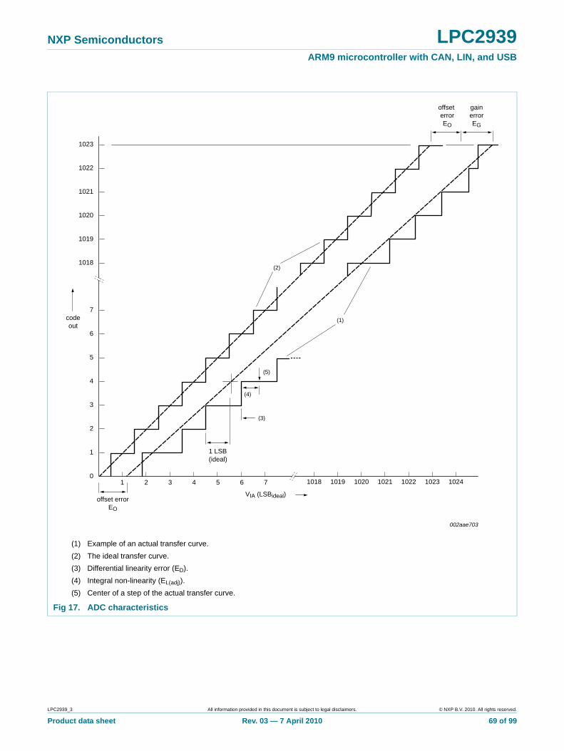
NXP Semiconductors LPC2939ARM9 microcontroller with CAN, LIN, and USB
(1) Example of an actual transfer curve.
(2) The ideal transfer curve.
(3) Differential linearity error (ED).
(4) Integral non-linearity (EL(adj)).
(5) Center of a step of the actual transfer curve.
Fig 17. ADC characteristics
002aae703
1023
1022
1021
1020
1019
(2)
(1)
10241018 1019 1020 1021 1022 102371 2 3 4 5 6
7
6
5
4
3
2
1
0
1018
(5)
(4)
(3)
1 LSB(ideal)
codeout
offset errorEO
gainerrorEG
offset errorEO
VIA (LSBideal)
LPC2939_3 All information provided in this document is subject to legal disclaimers. © NXP B.V. 2010. All rights reserved.
Product data sheet Rev. 03 — 7 April 2010 69 of 99
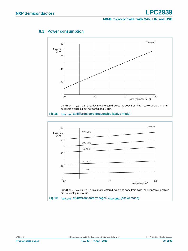
NXP Semiconductors LPC2939ARM9 microcontroller with CAN, LIN, and USB
8.1 Power consumption
Conditions: Tamb = 25 C; active mode entered executing code from flash; core voltage 1.8 V; all peripherals enabled but not configured to run.
Fig 18. IDD(CORE) at different core frequencies (active mode)
Conditions: Tamb = 25 C; active mode entered executing code from flash; all peripherals enabled but not configured to run.
Fig 19. IDD(CORE) at different core voltages VDD(CORE) (active mode)
core frequency (MHz)10 1309050
002aae241
40
20
60
80
IDD(CORE)(mA)
0
core voltage (V)1.7 1.91.8
002aae240
40
20
60
80
IDD(CORE)(mA)
0
10 MHz
40 MHz
80 MHz
100 MHz
125 MHz
LPC2939_3 All information provided in this document is subject to legal disclaimers. © NXP B.V. 2010. All rights reserved.
Product data sheet Rev. 03 — 7 April 2010 70 of 99
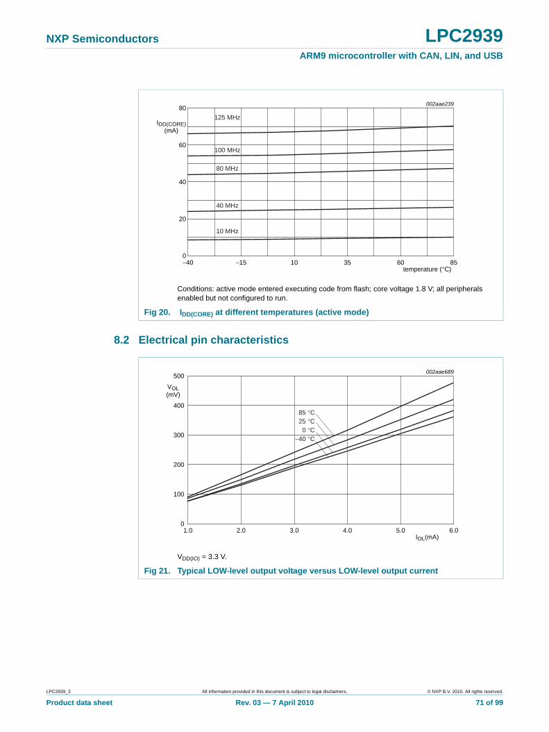
NXP Semiconductors LPC2939ARM9 microcontroller with CAN, LIN, and USB
8.2 Electrical pin characteristics
Conditions: active mode entered executing code from flash; core voltage 1.8 V; all peripherals enabled but not configured to run.
Fig 20. IDD(CORE) at different temperatures (active mode)
temperature (°C)−40 856010 35−15
002aae239
40
20
60
80
IDD(CORE)(mA)
0
10 MHz
80 MHz
100 MHz
40 MHz
125 MHz
VDD(IO) = 3.3 V.
Fig 21. Typical LOW-level output voltage versus LOW-level output current
002aae689
IOL(mA)1.0 6.04.03.0 5.02.0
200
400
100
300
500
VOL(mV)
0
85 °C25 °C
0 °C−40 °C
LPC2939_3 All information provided in this document is subject to legal disclaimers. © NXP B.V. 2010. All rights reserved.
Product data sheet Rev. 03 — 7 April 2010 71 of 99
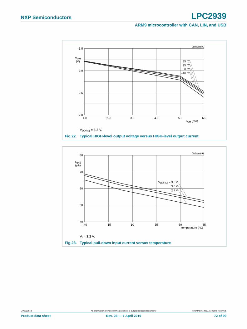
NXP Semiconductors LPC2939ARM9 microcontroller with CAN, LIN, and USB
VDD(IO) = 3.3 V.
Fig 22. Typical HIGH-level output voltage versus HIGH-level output current
VI = 3.3 V.
Fig 23. Typical pull-down input current versus temperature
IOH (mA)1.0 6.04.03.0 5.02.0
002aae690
2.5
3.0
3.5
VOH(V)
2.0
85 °C25 °C
0 °C−40 °C
002aae691
temperature (°C)−40 853510 60−15
50
70
60
80
II(pd)(μA)
40
VDD(IO) = 3.6 V3.0 V2.7 V
LPC2939_3 All information provided in this document is subject to legal disclaimers. © NXP B.V. 2010. All rights reserved.
Product data sheet Rev. 03 — 7 April 2010 72 of 99
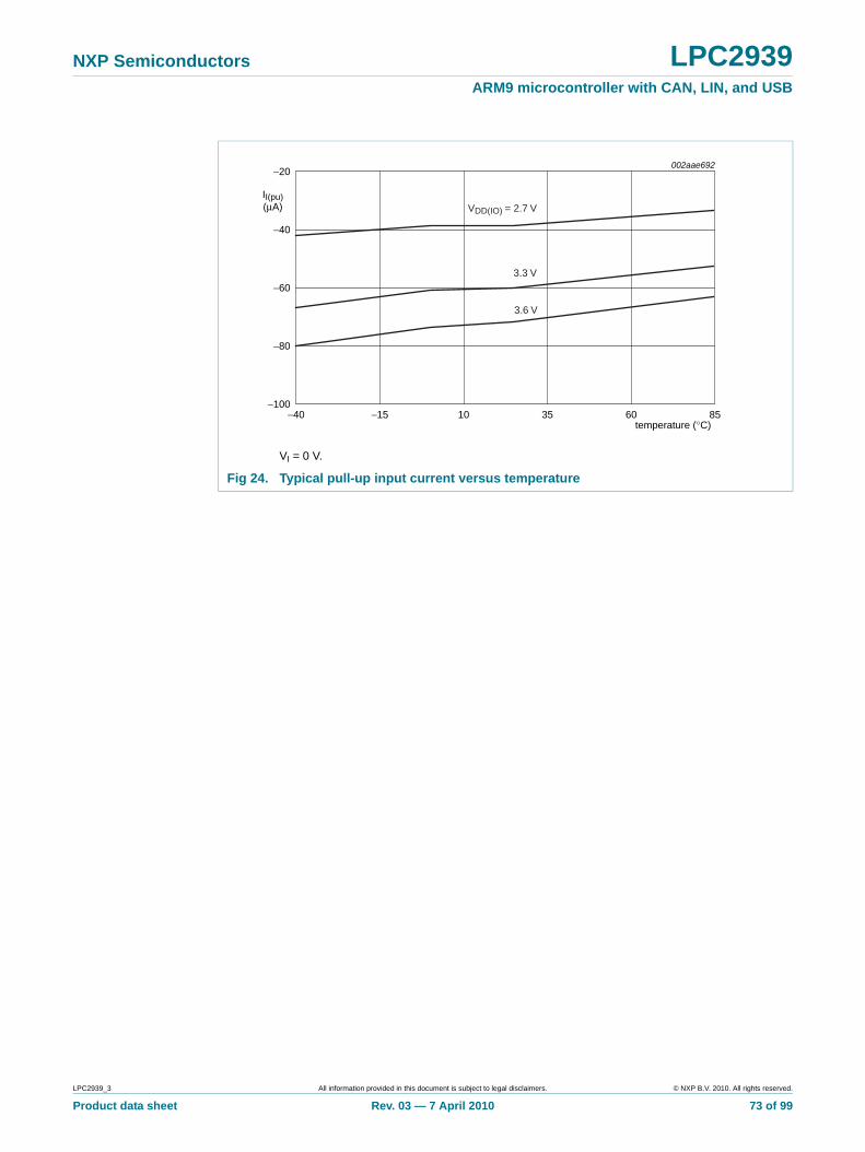
NXP Semiconductors LPC2939ARM9 microcontroller with CAN, LIN, and USB
VI = 0 V.
Fig 24. Typical pull-up input current versus temperature
002aae692
temperature (°C)−40 853510 60−15
−80
−40
−60
−20
II(pu)(μA)
−100
VDD(IO) = 2.7 V
3.3 V
3.6 V
LPC2939_3 All information provided in this document is subject to legal disclaimers. © NXP B.V. 2010. All rights reserved.
Product data sheet Rev. 03 — 7 April 2010 73 of 99
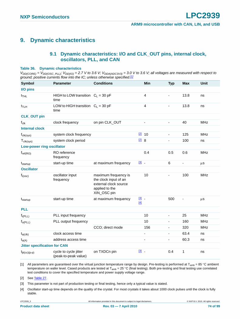
NXP Semiconductors LPC2939ARM9 microcontroller with CAN, LIN, and USB
9. Dynamic characteristics
9.1 Dynamic characteristics: I/O and CLK_OUT pins, internal clock, oscillators, PLL, and CAN
[1] All parameters are guaranteed over the virtual junction temperature range by design. Pre-testing is performed at Tamb = 85 C ambient temperature on wafer level. Cased products are tested at Tamb = 25 C (final testing). Both pre-testing and final testing use correlated test conditions to cover the specified temperature and power supply voltage range.
[2] See Table 27.
[3] This parameter is not part of production testing or final testing, hence only a typical value is stated.
[4] Oscillator start-up time depends on the quality of the crystal. For most crystals it takes about 1000 clock pulses until the clock is fully stable.
Table 36. Dynamic characteristicsVDD(CORE) = VDD(OSC_PLL); VDD(IO) = 2.7 V to 3.6 V; VDDA(ADC3V3) = 3.0 V to 3.6 V; all voltages are measured with respect to ground; positive currents flow into the IC; unless otherwise specified.[1]
Symbol Parameter Conditions Min Typ Max Unit
I/O pins
tTHL HIGH to LOW transition time
CL = 30 pF 4 - 13.8 ns
tTLH LOW to HIGH transition time
CL = 30 pF 4 - 13.8 ns
CLK_OUT pin
fclk clock frequency on pin CLK_OUT - - 40 MHz
Internal clock
fclk(sys) system clock frequency [2] 10 - 125 MHz
Tclk(sys) system clock period [2] 8 - 100 ns
Low-power ring oscillator
fref(RO) RO reference frequency
0.4 0.5 0.6 MHz
tstartup start-up time at maximum frequency [3] - 6 - s
Oscillator
fi(osc) oscillator input frequency
maximum frequency is the clock input of an external clock source applied to the XIN_OSC pin
10 - 100 MHz
tstartup start-up time at maximum frequency [3]
[4]- 500 - s
PLL
fi(PLL) PLL input frequency 10 - 25 MHz
fo(PLL) PLL output frequency 10 - 160 MHz
CCO; direct mode 156 - 320 MHz
ta(clk) clock access time - - 63.4 ns
ta(A) address access time - - 60.3 ns
Jitter specification for CAN
tjit(cc)(p-p) cycle to cycle jitter (peak-to-peak value)
on TXDCn pin [3] - 0.4 1 ns
LPC2939_3 All information provided in this document is subject to legal disclaimers. © NXP B.V. 2010. All rights reserved.
Product data sheet Rev. 03 — 7 April 2010 74 of 99
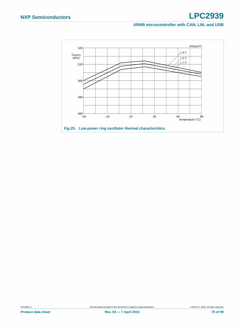
NXP Semiconductors LPC2939ARM9 microcontroller with CAN, LIN, and USB
Fig 25. Low-power ring oscillator thermal characteristics
temperature (°C)−40 856010 35−15
002aae373
500
490
510
520
fref(RO)(kHz)
480
1.9 V
1.8 V
1.7 V
LPC2939_3 All information provided in this document is subject to legal disclaimers. © NXP B.V. 2010. All rights reserved.
Product data sheet Rev. 03 — 7 April 2010 75 of 99
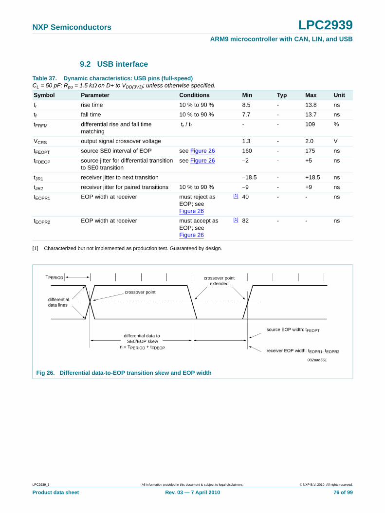
NXP Semiconductors LPC2939ARM9 microcontroller with CAN, LIN, and USB
9.2 USB interface
[1] Characterized but not implemented as production test. Guaranteed by design.
Table 37. Dynamic characteristics: USB pins (full-speed)CL = 50 pF; Rpu = 1.5 k on D+ to VDD(3V3); unless otherwise specified.
Symbol Parameter Conditions Min Typ Max Unit
tr rise time 10 % to 90 % 8.5 - 13.8 ns
tf fall time 10 % to 90 % 7.7 - 13.7 ns
tFRFM differential rise and fall time matching
tr / tf - - 109 %
VCRS output signal crossover voltage 1.3 - 2.0 V
tFEOPT source SE0 interval of EOP see Figure 26 160 - 175 ns
tFDEOP source jitter for differential transition to SE0 transition
see Figure 26 2 - +5 ns
tJR1 receiver jitter to next transition 18.5 - +18.5 ns
tJR2 receiver jitter for paired transitions 10 % to 90 % 9 - +9 ns
tEOPR1 EOP width at receiver must reject as EOP; see Figure 26
[1] 40 - - ns
tEOPR2 EOP width at receiver must accept as EOP; see Figure 26
[1] 82 - - ns
Fig 26. Differential data-to-EOP transition skew and EOP width
002aab561
TPERIOD
differentialdata lines
crossover point
source EOP width: tFEOPT
receiver EOP width: tEOPR1, tEOPR2
crossover pointextended
differential data to SE0/EOP skew
n × TPERIOD + tFDEOP
LPC2939_3 All information provided in this document is subject to legal disclaimers. © NXP B.V. 2010. All rights reserved.
Product data sheet Rev. 03 — 7 April 2010 76 of 99
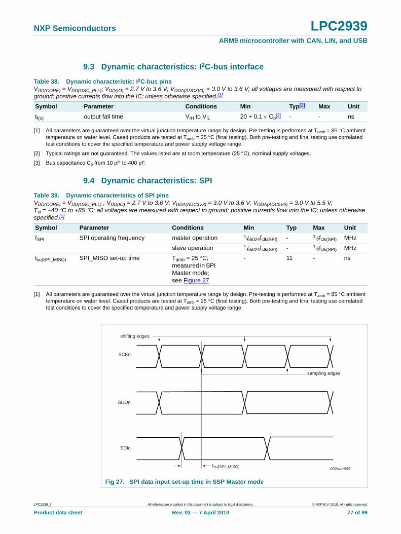
NXP Semiconductors LPC2939ARM9 microcontroller with CAN, LIN, and USB
9.3 Dynamic characteristics: I2C-bus interface
[1] All parameters are guaranteed over the virtual junction temperature range by design. Pre-testing is performed at Tamb = 85 C ambient temperature on wafer level. Cased products are tested at Tamb = 25 C (final testing). Both pre-testing and final testing use correlated test conditions to cover the specified temperature and power supply voltage range.
[2] Typical ratings are not guaranteed. The values listed are at room temperature (25 C), nominal supply voltages.
[3] Bus capacitance Cb from 10 pF to 400 pF.
9.4 Dynamic characteristics: SPI
[1] All parameters are guaranteed over the virtual junction temperature range by design. Pre-testing is performed at Tamb = 85 C ambient temperature on wafer level. Cased products are tested at Tamb = 25 C (final testing). Both pre-testing and final testing use correlated test conditions to cover the specified temperature and power supply voltage range.
Table 38. Dynamic characteristic: I2C-bus pinsVDD(CORE) = VDD(OSC_PLL); VDD(IO) = 2.7 V to 3.6 V; VDDA(ADC3V3) = 3.0 V to 3.6 V; all voltages are measured with respect to ground; positive currents flow into the IC; unless otherwise specified.[1]
Symbol Parameter Conditions Min Typ[2] Max Unit
tf(o) output fall time VIH to VIL 20 + 0.1 Cb[3] - - ns
Table 39. Dynamic characteristics of SPI pinsVDD(CORE) = VDD(OSC_PLL) ; VDD(IO) = 2.7 V to 3.6 V; VDDA(ADC3V3) = 3.0 V to 3.6 V; VDDA(ADC5V0) = 3.0 V to 5.5 V; Tvj = 40 C to +85 C; all voltages are measured with respect to ground; positive currents flow into the IC; unless otherwise specified.[1]
Symbol Parameter Conditions Min Typ Max Unit
fSPI SPI operating frequency master operation 165024fclk(SPI) - 12fclk(SPI) MHz
slave operation 165024fclk(SPI) - 14fclk(SPI) MHz
tsu(SPI_MISO) SPI_MISO set-up time Tamb = 25 C; measured in SPI Master mode; see Figure 27
- 11 - ns
Fig 27. SPI data input set-up time in SSP Master mode
tsu(SPI_MISO)
SCKn
shifting edges
SDOn
SDIn
002aae695
sampling edges
LPC2939_3 All information provided in this document is subject to legal disclaimers. © NXP B.V. 2010. All rights reserved.
Product data sheet Rev. 03 — 7 April 2010 77 of 99
NXP Semiconductors LPC2939ARM9 microcontroller with CAN, LIN, and USB
9.5 Dynamic characteristics: flash memory and EEPROM
[1] Number of program/erase cycles.
Table 40. Flash characteristicsTamb = 40 C to +85 C; VDD(CORE) = VDD(OSC_PLL); VDD(IO) = 2.7 V to 3.6 V; VDDA(ADC3V3) = 3.0 V to 3.6 V; all voltages are measured with respect to ground.
Symbol Parameter Conditions Min Typ Max Unit
Nendu endurance [1] 10000 - - cycles
tret retention time powered 10 - - years
unpowered 20 - - years
tprog programming time word 0.95 1 1.05 ms
ter erase time global 95 100 105 ms
sector 95 100 105 ms
tinit initialization time - - 150 s
twr(pg) page write time 0.95 1 1.05 ms
tfl(BIST) flash word BIST time - 38 70 ns
ta(clk) clock access time - - 63.4 ns
ta(A) address access time - - 60.3 ns
Table 41. EEPROM characteristicsTamb = 40 C to +85 C; VDD(CORE) = VDD(OSC_PLL); VDD(IO) = 2.7 V to 3.6 V; VDDA(ADC3V3) = 3.0 V to 3.6 V; all voltages are measured with respect to ground.
Symbol Parameter Conditions Min Typ Max Unit
fclk clock frequency 200 375 400 kHz
Nendu endurance 100000 500000 - cycles
tret retention time powered 10 - - years
LPC2939_3 All information provided in this document is subject to legal disclaimers. © NXP B.V. 2010. All rights reserved.
Product data sheet Rev. 03 — 7 April 2010 78 of 99
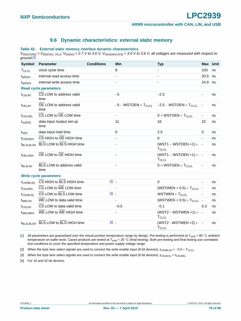
NXP Semiconductors LPC2939ARM9 microcontroller with CAN, LIN, and USB
9.6 Dynamic characteristics: external static memory
[1] All parameters are guaranteed over the virtual junction temperature range by design. Pre-testing is performed at Tamb = 85 C ambient temperature on wafer level. Cased products are tested at Tamb = 25 C (final testing). Both pre-testing and final testing use correlated test conditions to cover the specified temperature and power supply voltage range.
[2] When the byte lane select signals are used to connect the write enable input (8 bit devices), tCSHBLSH = 0.5 TCLCL.
[3] When the byte lane select signals are used to connect the write enable input (8 bit devices), tCSLBLSL = tCSLWEL.
[4] For 16 and 32 bit devices.
Table 42. External static memory interface dynamic characteristicsVDD(CORE) = VDD(OSC_PLL); VDD(IO) = 2.7 V to 3.6 V; VDDA(ADC3V3) = 3.0 V to 3.6 V; all voltages are measured with respect to ground.[1]
Symbol Parameter Conditions Min Typ Max Unit
TCLCL clock cycle time 8 - 100 ns
ta(R)int internal read access time - - 20.5 ns
ta(W)int internal write access time - - 24.9 ns
Read cycle parameters
tCSLAV CS LOW to address valid time
5 2.5 - ns
tOELAV OE LOW to address valid time
5 WSTOEN TCLCL 2.5 WSTOEN TCLCL - ns
tCSLOEL CS LOW to OE LOW time - 0 + WSTOEN TCLCL - ns
tsu(DQ) data input /output set-up time
11 16 22 ns
th(D) data input hold time 0 2.5 5 ns
tCSHOEH CS HIGH to OE HIGH time - 0 - ns
tBLSLBLSH BLS LOW to BLS HIGH time - (WST1 WSTOEN +1) TCLCL
- ns
tOELOEH OE LOW to OE HIGH time - (WST1 WSTOEN +1) TCLCL
- ns
tBLSLAV BLS LOW to address valid time
- 0 + WSTOEN TCLCL - ns
Write cycle parameters
tCSHBLSH CS HIGH to BLS HIGH time [2] - 0 - ns
tCSLWEL CS LOW to WE LOW time - (WSTWEN + 0.5) TCLCL - ns
tCSLBLSL CS LOW to BLS LOW time [3] - WSTWEN TCLCL - ns
tWELDV WE LOW to data valid time - (WSTWEN + 0.5) TCLCL - ns
tCSLDV CS LOW to data valid time 0.5 0.1 0.3 ns
tWELWEH WE LOW to WE HIGH time - (WST2 WSTWEN +1) TCLCL
- ns
tBLSLBLSH BLS LOW to BLS HIGH time [4] - (WST2 - WSTWEN +2) TCLCL
- ns
LPC2939_3 All information provided in this document is subject to legal disclaimers. © NXP B.V. 2010. All rights reserved.
Product data sheet Rev. 03 — 7 April 2010 79 of 99
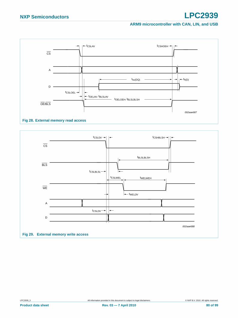
NXP Semiconductors LPC2939ARM9 microcontroller with CAN, LIN, and USB
Fig 28. External memory read access
CS
A
D
OE/BLS
tCSLAV
tOELAV, tBLSLAVtOELOEH, tBLSLBLSH
tCSLOEL
th(D)tsu(DQ)
tCSHOEH
002aae687
Fig 29. External memory write access
CS
A
D
WE
tCSLWEL
tWELDV
tCSLDV
tWELWEH
tBLSLBLSH
002aae688
tCSLBLSL
BLS
tCSLDV tCSHBLSH
LPC2939_3 All information provided in this document is subject to legal disclaimers. © NXP B.V. 2010. All rights reserved.
Product data sheet Rev. 03 — 7 April 2010 80 of 99
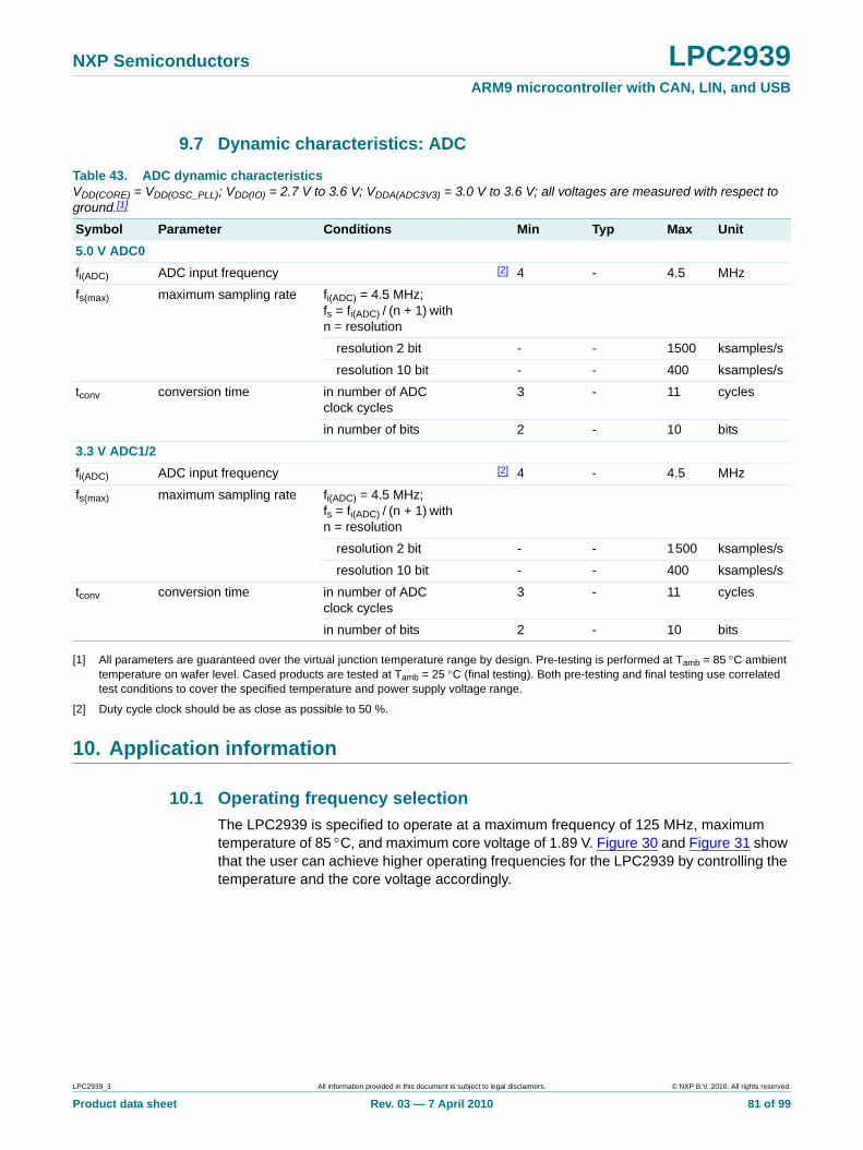
NXP Semiconductors LPC2939ARM9 microcontroller with CAN, LIN, and USB
9.7 Dynamic characteristics: ADC
[1] All parameters are guaranteed over the virtual junction temperature range by design. Pre-testing is performed at Tamb = 85 C ambient temperature on wafer level. Cased products are tested at Tamb = 25 C (final testing). Both pre-testing and final testing use correlated test conditions to cover the specified temperature and power supply voltage range.
[2] Duty cycle clock should be as close as possible to 50 %.
10. Application information
10.1 Operating frequency selection
The LPC2939 is specified to operate at a maximum frequency of 125 MHz, maximum temperature of 85 C, and maximum core voltage of 1.89 V. Figure 30 and Figure 31 show that the user can achieve higher operating frequencies for the LPC2939 by controlling the temperature and the core voltage accordingly.
Table 43. ADC dynamic characteristicsVDD(CORE) = VDD(OSC_PLL); VDD(IO) = 2.7 V to 3.6 V; VDDA(ADC3V3) = 3.0 V to 3.6 V; all voltages are measured with respect to ground.[1]
Symbol Parameter Conditions Min Typ Max Unit
5.0 V ADC0
fi(ADC) ADC input frequency [2] 4 - 4.5 MHz
fs(max) maximum sampling rate fi(ADC) = 4.5 MHz; fs = fi(ADC) / (n + 1) with n = resolution
resolution 2 bit - - 1500 ksamples/s
resolution 10 bit - - 400 ksamples/s
tconv conversion time in number of ADC clock cycles
3 - 11 cycles
in number of bits 2 - 10 bits
3.3 V ADC1/2
fi(ADC) ADC input frequency [2] 4 - 4.5 MHz
fs(max) maximum sampling rate fi(ADC) = 4.5 MHz; fs = fi(ADC) / (n + 1) with n = resolution
resolution 2 bit - - 1500 ksamples/s
resolution 10 bit - - 400 ksamples/s
tconv conversion time in number of ADC clock cycles
3 - 11 cycles
in number of bits 2 - 10 bits
LPC2939_3 All information provided in this document is subject to legal disclaimers. © NXP B.V. 2010. All rights reserved.
Product data sheet Rev. 03 — 7 April 2010 81 of 99
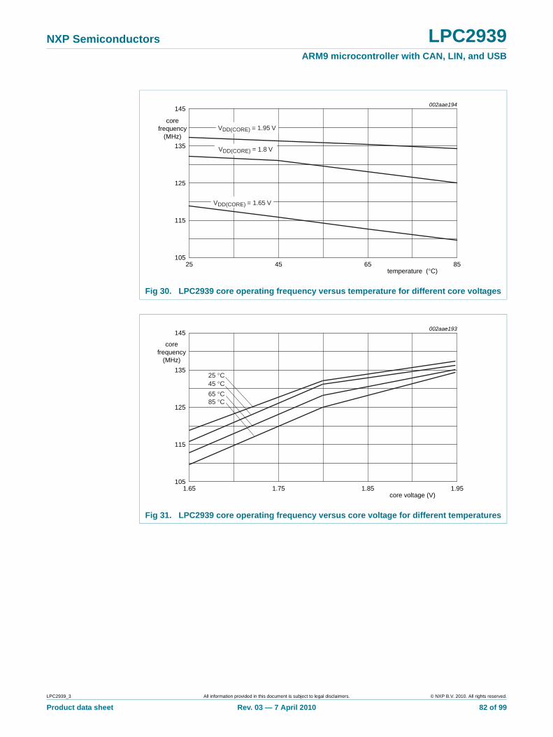
NXP Semiconductors LPC2939ARM9 microcontroller with CAN, LIN, and USB
Fig 30. LPC2939 core operating frequency versus temperature for different core voltages
Fig 31. LPC2939 core operating frequency versus core voltage for different temperatures
temperature (°C)25 856545
002aae194
125
115
135
145
corefrequency
(MHz)
105
VDD(CORE) = 1.95 V
VDD(CORE) = 1.8 V
VDD(CORE) = 1.65 V
core voltage (V)1.65 1.951.851.75
002aae193
125
115
135
145
corefrequency
(MHz)
105
25 °C45 °C65 °C85 °C
LPC2939_3 All information provided in this document is subject to legal disclaimers. © NXP B.V. 2010. All rights reserved.
Product data sheet Rev. 03 — 7 April 2010 82 of 99
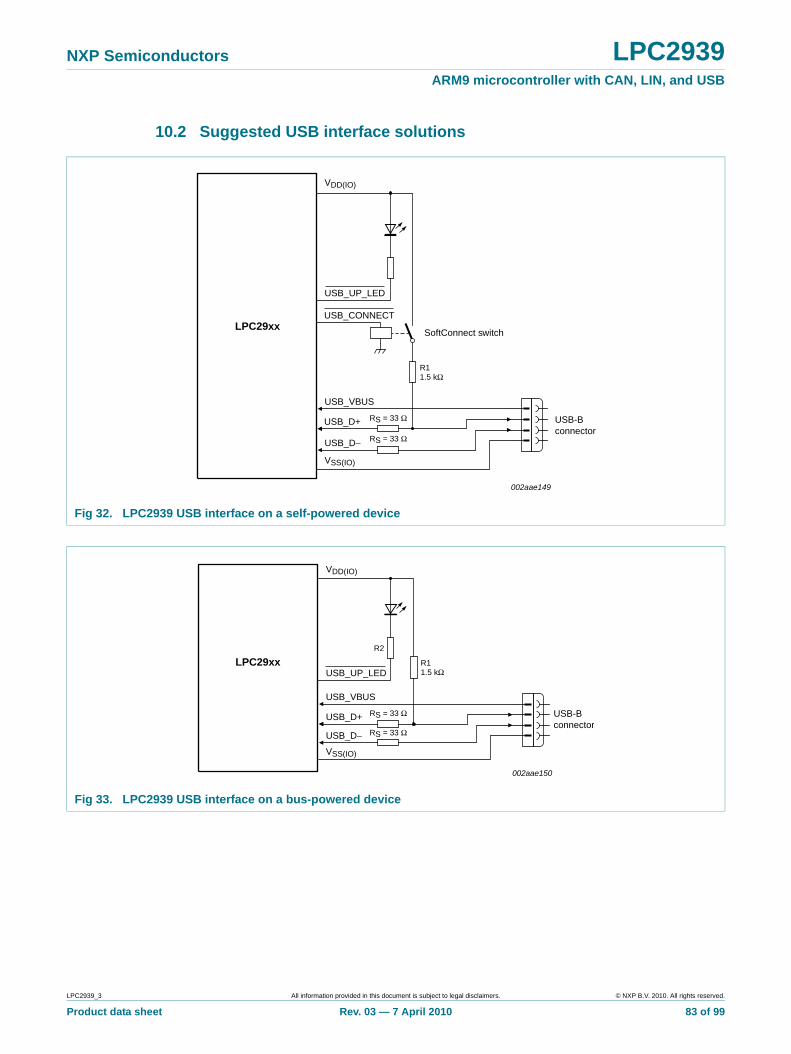
NXP Semiconductors LPC2939ARM9 microcontroller with CAN, LIN, and USB
10.2 Suggested USB interface solutions
Fig 32. LPC2939 USB interface on a self-powered device
LPC29xx
USB-Bconnector
USB_D+
SoftConnect switch
USB_D−
USB_VBUS
VSS(IO)
VDD(IO)
R11.5 kΩ
RS = 33 Ω
002aae149
RS = 33 Ω
USB_UP_LED
USB_CONNECT
Fig 33. LPC2939 USB interface on a bus-powered device
LPC29xx
VDD(IO)
R11.5 kΩ
R2
002aae150
USB-Bconnector
USB_D+
USB_D−
USB_VBUS
VSS(IO)
RS = 33 Ω
RS = 33 Ω
USB_UP_LED
LPC2939_3 All information provided in this document is subject to legal disclaimers. © NXP B.V. 2010. All rights reserved.
Product data sheet Rev. 03 — 7 April 2010 83 of 99
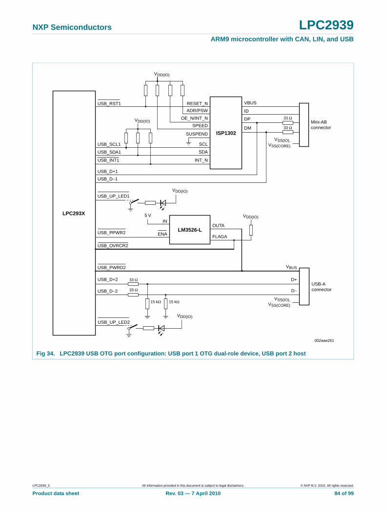
NXP Semiconductors LPC2939ARM9 microcontroller with CAN, LIN, and USB
Fig 34. LPC2939 USB OTG port configuration: USB port 1 OTG dual-role device, USB port 2 host
USB_UP_LED1
USB_D+1
USB_D−1
USB_PWRD2
USB_SDA1
USB_SCL1
USB_RST1
15 kΩ 15 kΩ
LPC293X
USB-Aconnector
Mini-ABconnector
33 Ω
33 Ω
33 Ω
33 Ω
VDD(IO)
VDD(IO)
VDD(IO)
USB_UP_LED2
VDD(IO)
USB_OVRCR2
LM3526-LENA
IN5 V
OUTA
FLAGA
VDD(IO)
D+
D−
VBUS
USB_PPWR2
USB_D+2
USB_D−2
002aae261
USB_INT1
RESET_N
ADR/PSW
SPEED
SUSPEND
OE_N/INT_N
SCL
SDA
INT_N
VBUS
ID
DP
DMISP1302
VSS(IO),VSS(CORE)
VSS(IO),VSS(CORE)
LPC2939_3 All information provided in this document is subject to legal disclaimers. © NXP B.V. 2010. All rights reserved.
Product data sheet Rev. 03 — 7 April 2010 84 of 99
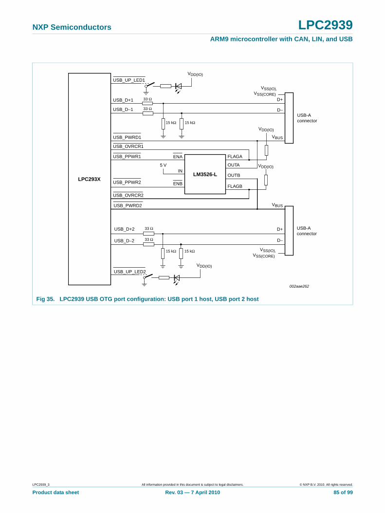
NXP Semiconductors LPC2939ARM9 microcontroller with CAN, LIN, and USB
Fig 35. LPC2939 USB OTG port configuration: USB port 1 host, USB port 2 host
USB_UP_LED1
USB_D+1
USB_D−1
USB_PWRD1
USB_PWRD2
15 kΩ
15 kΩ 15 kΩ
15 kΩ
LPC293X
USB-Aconnector
USB-Aconnector
33 Ω
33 Ω
33 Ω
33 Ω
002aae262
VDD(IO)
USB_UP_LED2
VDD(IO)
USB_OVRCR1
USB_OVRCR2
USB_PPWR1
LM3526-L
ENA
ENB
IN5 V
FLAGA
OUTA
OUTB
FLAGB
VDD(IO)
VDD(IO)
D+
D−
D+
D−
VBUS
VBUS
USB_PPWR2
USB_D+2
USB_D−2
VSS(IO),VSS(CORE)
VSS(IO),VSS(CORE)
LPC2939_3 All information provided in this document is subject to legal disclaimers. © NXP B.V. 2010. All rights reserved.
Product data sheet Rev. 03 — 7 April 2010 85 of 99
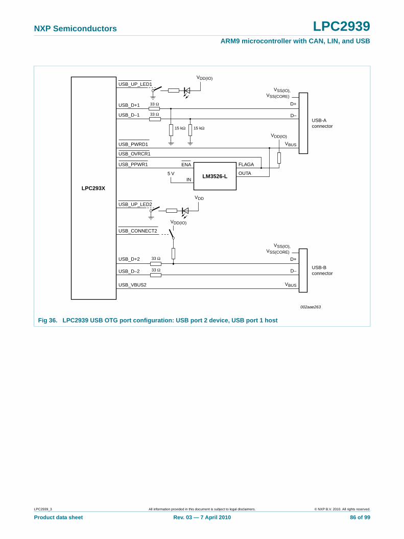
NXP Semiconductors LPC2939ARM9 microcontroller with CAN, LIN, and USB
Fig 36. LPC2939 USB OTG port configuration: USB port 2 device, USB port 1 host
USB_UP_LED1
USB_D+1
USB_D−1
USB_PWRD1
15 kΩ 15 kΩ
LPC293X
USB-Aconnector
USB-Bconnector
33 Ω
33 Ω
33 Ω
33 Ω
002aae263
VDD(IO)
USB_UP_LED2
USB_CONNECT2
VDD
VDD(IO)
USB_OVRCR1
USB_PPWR1
LM3526-L
ENA
IN5 V
FLAGA
OUTA
VDD(IO)
D+
D−
D+
D−
VBUS
USB_D+2
USB_D−2
USB_VBUS2 VBUS
VSS(IO),VSS(CORE)
VSS(IO),VSS(CORE)
LPC2939_3 All information provided in this document is subject to legal disclaimers. © NXP B.V. 2010. All rights reserved.
Product data sheet Rev. 03 — 7 April 2010 86 of 99
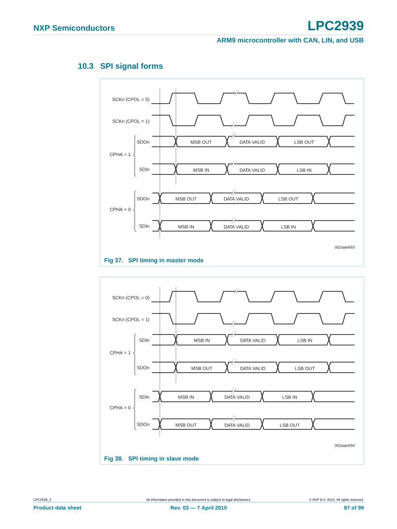
NXP Semiconductors LPC2939ARM9 microcontroller with CAN, LIN, and USB
10.3 SPI signal forms
Fig 37. SPI timing in master mode
Fig 38. SPI timing in slave mode
SCKn (CPOL = 0)
SDOn
SDIn
002aae693
MSB OUT LSB OUTDATA VALID
SCKn (CPOL = 1)
MSB IN LSB INDATA VALID
SDOn
SDIn
MSB OUT LSB OUTDATA VALID
MSB IN LSB INDATA VALID
CPHA = 0
CPHA = 1
SCKn (CPOL = 0)
SDIn
SDOn
002aae694
MSB IN LSB INDATA VALID
SCKn (CPOL = 1)
MSB OUT LSB OUTDATA VALID
SDIn
SDOn
MSB IN LSB INDATA VALID
MSB OUT LSB OUTDATA VALID
CPHA = 0
CPHA = 1
LPC2939_3 All information provided in this document is subject to legal disclaimers. © NXP B.V. 2010. All rights reserved.
Product data sheet Rev. 03 — 7 April 2010 87 of 99
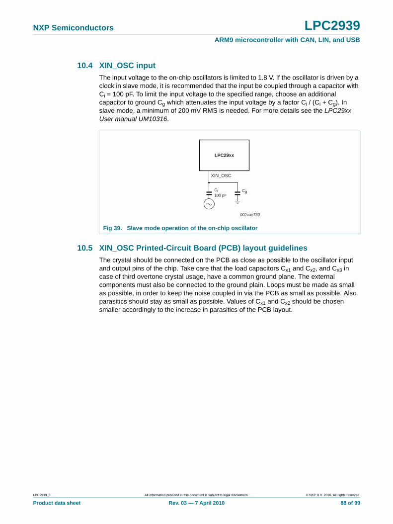
NXP Semiconductors LPC2939ARM9 microcontroller with CAN, LIN, and USB
10.4 XIN_OSC input
The input voltage to the on-chip oscillators is limited to 1.8 V. If the oscillator is driven by a clock in slave mode, it is recommended that the input be coupled through a capacitor with Ci = 100 pF. To limit the input voltage to the specified range, choose an additional capacitor to ground Cg which attenuates the input voltage by a factor Ci / (Ci + Cg). In slave mode, a minimum of 200 mV RMS is needed. For more details see the LPC29xx User manual UM10316.
10.5 XIN_OSC Printed-Circuit Board (PCB) layout guidelines
The crystal should be connected on the PCB as close as possible to the oscillator input and output pins of the chip. Take care that the load capacitors Cx1 and Cx2, and Cx3 in case of third overtone crystal usage, have a common ground plane. The external components must also be connected to the ground plain. Loops must be made as small as possible, in order to keep the noise coupled in via the PCB as small as possible. Also parasitics should stay as small as possible. Values of Cx1 and Cx2 should be chosen smaller accordingly to the increase in parasitics of the PCB layout.
Fig 39. Slave mode operation of the on-chip oscillator
LPC29xx
XIN_OSC
Ci100 pF
Cg
002aae730
LPC2939_3 All information provided in this document is subject to legal disclaimers. © NXP B.V. 2010. All rights reserved.
Product data sheet Rev. 03 — 7 April 2010 88 of 99
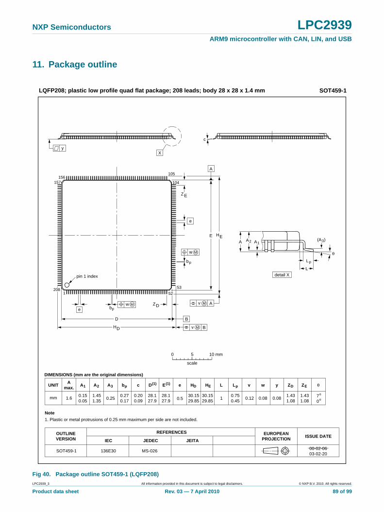
NXP Semiconductors LPC2939ARM9 microcontroller with CAN, LIN, and USB
11. Package outline
Fig 40. Package outline SOT459-1 (LQFP208)
UNIT A1 A2 A3 bp c E(1) e HE L Lp Zywv θ
REFERENCESOUTLINEVERSION
EUROPEANPROJECTION ISSUE DATE
IEC JEDEC JEITA
mm 0.150.05
1.451.35
0.250.270.17
0.200.09
28.127.9 0.5
30.1529.85
1.431.08
70
o
o0.080.121 0.08
DIMENSIONS (mm are the original dimensions)
Note
1. Plastic or metal protrusions of 0.25 mm maximum per side are not included.
0.750.45
SOT459-1 136E30 MS-026 00-02-0603-02-20
D(1)
28.127.9
HD
30.1529.85
EZ
1.431.08
D
pin 1 index
bpe
θ
EA1A
Lp
detail XL
(A )3
B
52
c
DH
bp
EHA2
v M B
D
ZD
A
ZE
e
v M A
X
1208
157156
105
104
53
y
w M
w M
0 5 10 mm
scale
LQFP208; plastic low profile quad flat package; 208 leads; body 28 x 28 x 1.4 mm SOT459-1
Amax.
1.6
LPC2939_3 All information provided in this document is subject to legal disclaimers. © NXP B.V. 2010. All rights reserved.
Product data sheet Rev. 03 — 7 April 2010 89 of 99
NXP Semiconductors LPC2939ARM9 microcontroller with CAN, LIN, and USB
12. Soldering of SMD packages
This text provides a very brief insight into a complex technology. A more in-depth account of soldering ICs can be found in Application Note AN10365 “Surface mount reflow soldering description”.
12.1 Introduction to soldering
Soldering is one of the most common methods through which packages are attached to Printed Circuit Boards (PCBs), to form electrical circuits. The soldered joint provides both the mechanical and the electrical connection. There is no single soldering method that is ideal for all IC packages. Wave soldering is often preferred when through-hole and Surface Mount Devices (SMDs) are mixed on one printed wiring board; however, it is not suitable for fine pitch SMDs. Reflow soldering is ideal for the small pitches and high densities that come with increased miniaturization.
12.2 Wave and reflow soldering
Wave soldering is a joining technology in which the joints are made by solder coming from a standing wave of liquid solder. The wave soldering process is suitable for the following:
• Through-hole components
• Leaded or leadless SMDs, which are glued to the surface of the printed circuit board
Not all SMDs can be wave soldered. Packages with solder balls, and some leadless packages which have solder lands underneath the body, cannot be wave soldered. Also, leaded SMDs with leads having a pitch smaller than ~0.6 mm cannot be wave soldered, due to an increased probability of bridging.
The reflow soldering process involves applying solder paste to a board, followed by component placement and exposure to a temperature profile. Leaded packages, packages with solder balls, and leadless packages are all reflow solderable.
Key characteristics in both wave and reflow soldering are:
• Board specifications, including the board finish, solder masks and vias
• Package footprints, including solder thieves and orientation
• The moisture sensitivity level of the packages
• Package placement
• Inspection and repair
• Lead-free soldering versus SnPb soldering
12.3 Wave soldering
Key characteristics in wave soldering are:
• Process issues, such as application of adhesive and flux, clinching of leads, board transport, the solder wave parameters, and the time during which components are exposed to the wave
• Solder bath specifications, including temperature and impurities
LPC2939_3 All information provided in this document is subject to legal disclaimers. © NXP B.V. 2010. All rights reserved.
Product data sheet Rev. 03 — 7 April 2010 90 of 99
NXP Semiconductors LPC2939ARM9 microcontroller with CAN, LIN, and USB
12.4 Reflow soldering
Key characteristics in reflow soldering are:
• Lead-free versus SnPb soldering; note that a lead-free reflow process usually leads to higher minimum peak temperatures (see Figure 41) than a SnPb process, thus reducing the process window
• Solder paste printing issues including smearing, release, and adjusting the process window for a mix of large and small components on one board
• Reflow temperature profile; this profile includes preheat, reflow (in which the board is heated to the peak temperature) and cooling down. It is imperative that the peak temperature is high enough for the solder to make reliable solder joints (a solder paste characteristic). In addition, the peak temperature must be low enough that the packages and/or boards are not damaged. The peak temperature of the package depends on package thickness and volume and is classified in accordance with Table 44 and 45
Moisture sensitivity precautions, as indicated on the packing, must be respected at all times.
Studies have shown that small packages reach higher temperatures during reflow soldering, see Figure 41.
Table 44. SnPb eutectic process (from J-STD-020C)
Package thickness (mm) Package reflow temperature (C)
Volume (mm3)
< 350 350
< 2.5 235 220
2.5 220 220
Table 45. Lead-free process (from J-STD-020C)
Package thickness (mm) Package reflow temperature (C)
Volume (mm3)
< 350 350 to 2000 > 2000
< 1.6 260 260 260
1.6 to 2.5 260 250 245
> 2.5 250 245 245
LPC2939_3 All information provided in this document is subject to legal disclaimers. © NXP B.V. 2010. All rights reserved.
Product data sheet Rev. 03 — 7 April 2010 91 of 99
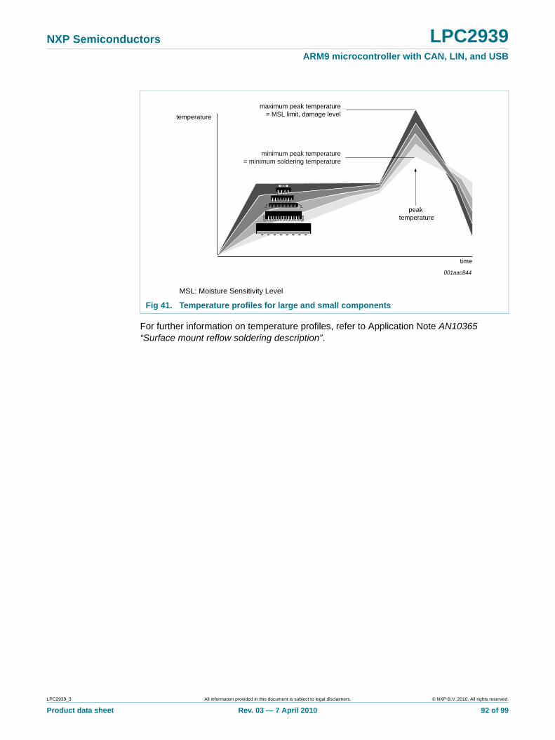
NXP Semiconductors LPC2939ARM9 microcontroller with CAN, LIN, and USB
For further information on temperature profiles, refer to Application Note AN10365 “Surface mount reflow soldering description”.
MSL: Moisture Sensitivity Level
Fig 41. Temperature profiles for large and small components
001aac844
temperature
time
minimum peak temperature= minimum soldering temperature
maximum peak temperature= MSL limit, damage level
peak temperature
LPC2939_3 All information provided in this document is subject to legal disclaimers. © NXP B.V. 2010. All rights reserved.
Product data sheet Rev. 03 — 7 April 2010 92 of 99
NXP Semiconductors LPC2939ARM9 microcontroller with CAN, LIN, and USB
13. Abbreviations
Table 46. Abbreviations list
Abbreviation Description
ADC Analog-to-Digital Converter
AF Acceptance Filter
AHB Advanced High-performance Bus
AMBA Advanced Microcontroller Bus Architecture
APB ARM Peripheral Bus
BIST Built-In Self Test
CAN Controller Area Network
CCO Current Controlled Oscillator
CISC Complex Instruction Set Computers
DMA Direct Memory Access
DSP Digital Signal Processing
DTL Device Transaction Level
EMI ElectroMagnetic Interference
EOP End Of Packet
ETB Embedded Trace Buffer
ETM Embedded Trace Macrocell
FDIV Fractional Divider
FIQ Fast Interrupt reQuest
GPDMA General Purpose DMA
GPIO General Purpose Input/Output
LIN Local Interconnect Network
LSB Least Significant Bit
LUT Look-Up Table
MAC Media Access Control
MSB Most Significant Bit
MSC Modulation and Sampling Control
MSCSS Modulation and Sampling Control SubSystem
MTMR MSCSS TiMeR
OHCI Open Host Controller Interface
OTG On-The-Go
PCR Power Control and Reset system
PHY PHYsical layer
PLL Phase-Locked Loop
POR Power-On Reset
PWM Pulse-Width Modulator
QEI Quadrature Encoder Interface
Q-SPI Queued-SPI
RISC Reduced Instruction Set Computer
SCU System Control Unit
LPC2939_3 All information provided in this document is subject to legal disclaimers. © NXP B.V. 2010. All rights reserved.
Product data sheet Rev. 03 — 7 April 2010 93 of 99
NXP Semiconductors LPC2939ARM9 microcontroller with CAN, LIN, and USB
14. References
[1] UM10316 — LPC29xx user manual.
[2] ARM — ARM web site.
[3] ARM-SSP — ARM primecell synchronous serial port (PL022) technical reference manual.
[4] CAN — ISO 11898-1: 2002 road vehicles - Controller Area Network (CAN) - part 1: data link layer and physical signalling.
[5] LIN — LIN specification package, revision 2.0.
SFSP SCU Function Select Port
SPI Serial Peripheral Interface
SSP Synchronous Serial Port
TAP Test Access Port
TCM Tightly-Coupled Memory
TTL Transistor-Transistor Logic
UART Universal Asynchronous Receiver Transmitter
USB Universal Serial Bus
WDT WatchDog Timer
Table 46. Abbreviations list …continued
Abbreviation Description
LPC2939_3 All information provided in this document is subject to legal disclaimers. © NXP B.V. 2010. All rights reserved.
Product data sheet Rev. 03 — 7 April 2010 94 of 99
NXP Semiconductors LPC2939ARM9 microcontroller with CAN, LIN, and USB
15. Revision history
Table 47. Revision history
Document ID Release date Data sheet status Change notice Supersedes
LPC2939_3 20100407 Product data sheet - LPC2939_2
Modifications • Table 3: Pin description for pins 187 (GPIO 4, pin 15) and 188 (GPIO 5, pin 15) corrected.
• USB logo added.
• Document template updated.
LPC2939_2 20091207 Product data sheet - LPC2939_1
Modifications • Table 3: Changed P1[31] to P1[30] for pin 29
LPC2939_1 20090611 Preliminary data sheet - -
LPC2939_3 All information provided in this document is subject to legal disclaimers. © NXP B.V. 2010. All rights reserved.
Product data sheet Rev. 03 — 7 April 2010 95 of 99
NXP Semiconductors LPC2939ARM9 microcontroller with CAN, LIN, and USB
16. Legal information
16.1 Data sheet status
[1] Please consult the most recently issued document before initiating or completing a design.
[2] The term ‘short data sheet’ is explained in section “Definitions”.
[3] The product status of device(s) described in this document may have changed since this document was published and may differ in case of multiple devices. The latest product status information is available on the Internet at URL http://www.nxp.com.
16.2 Definitions
Draft — The document is a draft version only. The content is still under internal review and subject to formal approval, which may result in modifications or additions. NXP Semiconductors does not give any representations or warranties as to the accuracy or completeness of information included herein and shall have no liability for the consequences of use of such information.
Short data sheet — A short data sheet is an extract from a full data sheet with the same product type number(s) and title. A short data sheet is intended for quick reference only and should not be relied upon to contain detailed and full information. For detailed and full information see the relevant full data sheet, which is available on request via the local NXP Semiconductors sales office. In case of any inconsistency or conflict with the short data sheet, the full data sheet shall prevail.
Product specification — The information and data provided in a Product data sheet shall define the specification of the product as agreed between NXP Semiconductors and its customer, unless NXP Semiconductors and customer have explicitly agreed otherwise in writing. In no event however, shall an agreement be valid in which the NXP Semiconductors product is deemed to offer functions and qualities beyond those described in the Product data sheet.
16.3 Disclaimers
Limited warranty and liability — Information in this document is believed to be accurate and reliable. However, NXP Semiconductors does not give any representations or warranties, expressed or implied, as to the accuracy or completeness of such information and shall have no liability for the consequences of use of such information.
In no event shall NXP Semiconductors be liable for any indirect, incidental, punitive, special or consequential damages (including - without limitation - lost profits, lost savings, business interruption, costs related to the removal or replacement of any products or rework charges) whether or not such damages are based on tort (including negligence), warranty, breach of contract or any other legal theory.
Notwithstanding any damages that customer might incur for any reason whatsoever, NXP Semiconductors’ aggregate and cumulative liability towards customer for the products described herein shall be limited in accordance with the Terms and conditions of commercial sale of NXP Semiconductors.
Right to make changes — NXP Semiconductors reserves the right to make changes to information published in this document, including without limitation specifications and product descriptions, at any time and without notice. This document supersedes and replaces all information supplied prior to the publication hereof.
Suitability for use — NXP Semiconductors products are not designed, authorized or warranted to be suitable for use in medical, military, aircraft, space or life support equipment, nor in applications where failure or
malfunction of an NXP Semiconductors product can reasonably be expected to result in personal injury, death or severe property or environmental damage. NXP Semiconductors accepts no liability for inclusion and/or use of NXP Semiconductors products in such equipment or applications and therefore such inclusion and/or use is at the customer’s own risk.
Applications — Applications that are described herein for any of these products are for illustrative purposes only. NXP Semiconductors makes no representation or warranty that such applications will be suitable for the specified use without further testing or modification.
NXP Semiconductors does not accept any liability related to any default, damage, costs or problem which is based on a weakness or default in the customer application/use or the application/use of customer’s third party customer(s) (hereinafter both referred to as “Application”). It is customer’s sole responsibility to check whether the NXP Semiconductors product is suitable and fit for the Application planned. Customer has to do all necessary testing for the Application in order to avoid a default of the Application and the product. NXP Semiconductors does not accept any liability in this respect.
Limiting values — Stress above one or more limiting values (as defined in the Absolute Maximum Ratings System of IEC 60134) will cause permanent damage to the device. Limiting values are stress ratings only and (proper) operation of the device at these or any other conditions above those given in the Recommended operating conditions section (if present) or the Characteristics sections of this document is not warranted. Constant or repeated exposure to limiting values will permanently and irreversibly affect the quality and reliability of the device.
Terms and conditions of commercial sale — NXP Semiconductors products are sold subject to the general terms and conditions of commercial sale, as published at http://www.nxp.com/profile/terms, unless otherwise agreed in a valid written individual agreement. In case an individual agreement is concluded only the terms and conditions of the respective agreement shall apply. NXP Semiconductors hereby expressly objects to applying the customer’s general terms and conditions with regard to the purchase of NXP Semiconductors products by customer.
No offer to sell or license — Nothing in this document may be interpreted or construed as an offer to sell products that is open for acceptance or the grant, conveyance or implication of any license under any copyrights, patents or other industrial or intellectual property rights.
Export control — This document as well as the item(s) described herein may be subject to export control regulations. Export might require a prior authorization from national authorities.
Quick reference data — The Quick reference data is an extract of the product data given in the Limiting values and Characteristics sections of this document, and as such is not complete, exhaustive or legally binding.
Non-automotive qualified products — Unless this data sheet expressly states that this specific NXP Semiconductors product is automotive qualified, the product is not suitable for automotive use. It is neither qualified nor tested in accordance with automotive testing or application requirements. NXP Semiconductors accepts no liability for inclusion and/or use of non-automotive qualified products in automotive equipment or applications.
Document status[1][2] Product status[3] Definition
Objective [short] data sheet Development This document contains data from the objective specification for product development.
Preliminary [short] data sheet Qualification This document contains data from the preliminary specification.
Product [short] data sheet Production This document contains the product specification.
LPC2939_3 All information provided in this document is subject to legal disclaimers. © NXP B.V. 2010. All rights reserved.
Product data sheet Rev. 03 — 7 April 2010 96 of 99
NXP Semiconductors LPC2939ARM9 microcontroller with CAN, LIN, and USB
In the event that customer uses the product for design-in and use in automotive applications to automotive specifications and standards, customer (a) shall use the product without NXP Semiconductors’ warranty of the product for such automotive applications, use and specifications, and (b) whenever customer uses the product for automotive applications beyond NXP Semiconductors’ specifications such use shall be solely at customer’s own risk, and (c) customer fully indemnifies NXP Semiconductors for any liability, damages or failed product claims resulting from customer design and use of the product for automotive applications beyond NXP Semiconductors’ standard warranty and NXP Semiconductors’ product specifications.
16.4 TrademarksNotice: All referenced brands, product names, service names and trademarks are the property of their respective owners.
I2C-bus — logo is a trademark of NXP B.V.
17. Contact information
For more information, please visit: http://www.nxp.com
For sales office addresses, please send an email to: [email protected]
LPC2939_3 All information provided in this document is subject to legal disclaimers. © NXP B.V. 2010. All rights reserved.
Product data sheet Rev. 03 — 7 April 2010 97 of 99
NXP Semiconductors LPC2939ARM9 microcontroller with CAN, LIN, and USB
18. Contents
1 General description . . . . . . . . . . . . . . . . . . . . . . 1
2 Features and benefits . . . . . . . . . . . . . . . . . . . . 1
3 Ordering information. . . . . . . . . . . . . . . . . . . . . 33.1 Ordering options . . . . . . . . . . . . . . . . . . . . . . . . 3
4 Block diagram . . . . . . . . . . . . . . . . . . . . . . . . . . 4
5 Pinning information. . . . . . . . . . . . . . . . . . . . . . 55.1 Pinning . . . . . . . . . . . . . . . . . . . . . . . . . . . . . . . 55.2 Pin description . . . . . . . . . . . . . . . . . . . . . . . . . 55.2.1 General description . . . . . . . . . . . . . . . . . . . . . 55.2.2 LQFP208 pin assignment . . . . . . . . . . . . . . . . . 5
6 Functional description . . . . . . . . . . . . . . . . . . 146.1 Architectural overview . . . . . . . . . . . . . . . . . . 146.2 ARM968E-S processor . . . . . . . . . . . . . . . . . . 146.3 On-chip flash memory system . . . . . . . . . . . . 156.4 On-chip static RAM. . . . . . . . . . . . . . . . . . . . . 156.5 Memory map. . . . . . . . . . . . . . . . . . . . . . . . . . 166.6 Reset, debug, test, and power description . . . 176.6.1 Reset and power-up behavior . . . . . . . . . . . . 176.6.2 Reset strategy . . . . . . . . . . . . . . . . . . . . . . . . 176.6.3 IEEE 1149.1 interface pins (JTAG boundary-scan
test). . . . . . . . . . . . . . . . . . . . . . . . . . . . . . . . . 176.6.3.1 ETM/ETB . . . . . . . . . . . . . . . . . . . . . . . . . . . . 186.6.4 Power supply pins . . . . . . . . . . . . . . . . . . . . . 186.7 Clocking strategy . . . . . . . . . . . . . . . . . . . . . . 186.7.1 Clock architecture. . . . . . . . . . . . . . . . . . . . . . 186.7.2 Base clock and branch clock relationship. . . . 206.8 Flash memory controller . . . . . . . . . . . . . . . . . 226.8.1 Functional description. . . . . . . . . . . . . . . . . . . 226.8.2 Flash layout . . . . . . . . . . . . . . . . . . . . . . . . . . 236.8.3 Flash bridge wait-states . . . . . . . . . . . . . . . . . 246.8.4 Pin description . . . . . . . . . . . . . . . . . . . . . . . . 246.8.5 Clock description . . . . . . . . . . . . . . . . . . . . . . 256.8.6 EEPROM . . . . . . . . . . . . . . . . . . . . . . . . . . . . 256.9 External Static Memory Controller (SMC). . . . 256.9.1 Description . . . . . . . . . . . . . . . . . . . . . . . . . . . 256.9.2 Pin description . . . . . . . . . . . . . . . . . . . . . . . . 266.9.3 Clock description . . . . . . . . . . . . . . . . . . . . . . 266.9.4 External memory timing diagrams . . . . . . . . . 266.10 General Purpose DMA (GPDMA) controller . . 286.10.1 DMA support for peripherals. . . . . . . . . . . . . . 286.10.2 Clock description . . . . . . . . . . . . . . . . . . . . . . 296.11 USB interface . . . . . . . . . . . . . . . . . . . . . . . . . 296.11.1 USB device controller . . . . . . . . . . . . . . . . . . . 296.11.2 USB OTG controller . . . . . . . . . . . . . . . . . . . . 296.11.3 USB host controller. . . . . . . . . . . . . . . . . . . . . 306.11.3.1 Features . . . . . . . . . . . . . . . . . . . . . . . . . . . . . 306.11.4 Pin description . . . . . . . . . . . . . . . . . . . . . . . . 306.11.5 Clock description . . . . . . . . . . . . . . . . . . . . . . 316.12 General subsystem. . . . . . . . . . . . . . . . . . . . . 316.12.1 General subsystem clock description . . . . . . . 316.12.2 Chip and feature identification . . . . . . . . . . . . 316.12.3 System Control Unit (SCU). . . . . . . . . . . . . . . 316.12.4 Event router . . . . . . . . . . . . . . . . . . . . . . . . . . 316.12.4.1 Pin description . . . . . . . . . . . . . . . . . . . . . . . . 326.13 Peripheral subsystem . . . . . . . . . . . . . . . . . . . 32
6.13.1 Peripheral subsystem clock description. . . . . 326.13.2 Watchdog timer . . . . . . . . . . . . . . . . . . . . . . . 336.13.2.1 Functional description . . . . . . . . . . . . . . . . . . 336.13.2.2 Clock description . . . . . . . . . . . . . . . . . . . . . . 336.13.3 Timer . . . . . . . . . . . . . . . . . . . . . . . . . . . . . . . 336.13.3.1 Pin description . . . . . . . . . . . . . . . . . . . . . . . . 346.13.3.2 Clock description . . . . . . . . . . . . . . . . . . . . . . 356.13.4 UARTs . . . . . . . . . . . . . . . . . . . . . . . . . . . . . . 356.13.4.1 Pin description . . . . . . . . . . . . . . . . . . . . . . . . 356.13.4.2 Clock description . . . . . . . . . . . . . . . . . . . . . . 366.13.5 Serial peripheral interface (SPI). . . . . . . . . . . 366.13.5.1 Functional description . . . . . . . . . . . . . . . . . . 366.13.5.2 Pin description . . . . . . . . . . . . . . . . . . . . . . . . 376.13.5.3 Clock description . . . . . . . . . . . . . . . . . . . . . . 376.13.6 General-Purpose I/O (GPIO) . . . . . . . . . . . . . 376.13.6.1 Functional description . . . . . . . . . . . . . . . . . . 386.13.6.2 Pin description . . . . . . . . . . . . . . . . . . . . . . . . 386.13.6.3 Clock description . . . . . . . . . . . . . . . . . . . . . . 386.14 Networking subsystem. . . . . . . . . . . . . . . . . . 386.14.1 CAN gateway . . . . . . . . . . . . . . . . . . . . . . . . . 386.14.1.1 Global acceptance filter . . . . . . . . . . . . . . . . . 396.14.1.2 Pin description . . . . . . . . . . . . . . . . . . . . . . . . 396.14.2 LIN . . . . . . . . . . . . . . . . . . . . . . . . . . . . . . . . . 396.14.2.1 Pin description . . . . . . . . . . . . . . . . . . . . . . . . 396.14.3 I2C-bus serial I/O controllers . . . . . . . . . . . . . 406.14.3.1 Pin description . . . . . . . . . . . . . . . . . . . . . . . . 406.15 Modulation and Sampling Control SubSystem
(MSCSS) . . . . . . . . . . . . . . . . . . . . . . . . . . . . 406.15.1 Functional description . . . . . . . . . . . . . . . . . . 416.15.2 Pin description . . . . . . . . . . . . . . . . . . . . . . . . 436.15.3 Clock description . . . . . . . . . . . . . . . . . . . . . . 436.15.4 Analog-to-digital converter . . . . . . . . . . . . . . . 436.15.4.1 Functional description . . . . . . . . . . . . . . . . . . 446.15.4.2 Pin description . . . . . . . . . . . . . . . . . . . . . . . . 446.15.4.3 Clock description . . . . . . . . . . . . . . . . . . . . . . 456.15.5 Pulse Width Modulator (PWM). . . . . . . . . . . . 456.15.5.1 Functional description . . . . . . . . . . . . . . . . . . 466.15.5.2 Synchronizing the PWM counters . . . . . . . . . 476.15.5.3 Master and slave mode . . . . . . . . . . . . . . . . . 486.15.5.4 Pin description . . . . . . . . . . . . . . . . . . . . . . . . 486.15.5.5 Clock description . . . . . . . . . . . . . . . . . . . . . . 486.15.6 Timers in the MSCSS. . . . . . . . . . . . . . . . . . . 486.15.6.1 Pin description . . . . . . . . . . . . . . . . . . . . . . . . 496.15.6.2 Clock description . . . . . . . . . . . . . . . . . . . . . . 496.15.7 Quadrature Encoder Interface (QEI) . . . . . . . 496.15.7.1 Pin description . . . . . . . . . . . . . . . . . . . . . . . . 506.15.7.2 Clock description . . . . . . . . . . . . . . . . . . . . . . 506.16 Power, Clock and Reset control SubSystem
(PCRSS) . . . . . . . . . . . . . . . . . . . . . . . . . . . . 506.16.1 Clock description . . . . . . . . . . . . . . . . . . . . . . 516.16.2 Clock Generation Unit (CGU0) . . . . . . . . . . . 526.16.2.1 Functional description . . . . . . . . . . . . . . . . . . 526.16.2.2 PLL functional description . . . . . . . . . . . . . . . 556.16.2.3 Pin description . . . . . . . . . . . . . . . . . . . . . . . . 566.16.3 Clock generation for USB (CGU1) . . . . . . . . . 576.16.3.1 Pin description . . . . . . . . . . . . . . . . . . . . . . . . 57
LPC2939_3 All information provided in this document is subject to legal disclaimers. © NXP B.V. 2010. All rights reserved.
Product data sheet Rev. 03 — 7 April 2010 98 of 99
NXP Semiconductors LPC2939ARM9 microcontroller with CAN, LIN, and USB
6.16.4 Reset Generation Unit (RGU). . . . . . . . . . . . . 576.16.4.1 Functional description. . . . . . . . . . . . . . . . . . . 586.16.4.2 Pin description . . . . . . . . . . . . . . . . . . . . . . . . 586.16.5 Power Management Unit (PMU). . . . . . . . . . . 596.16.5.1 Functional description. . . . . . . . . . . . . . . . . . . 596.17 Vectored interrupt controller . . . . . . . . . . . . . . 616.17.1 Functional description. . . . . . . . . . . . . . . . . . . 626.17.2 Clock description . . . . . . . . . . . . . . . . . . . . . . 62
7 Limiting values. . . . . . . . . . . . . . . . . . . . . . . . . 63
8 Static characteristics. . . . . . . . . . . . . . . . . . . . 658.1 Power consumption . . . . . . . . . . . . . . . . . . . . 708.2 Electrical pin characteristics . . . . . . . . . . . . . . 71
9 Dynamic characteristics . . . . . . . . . . . . . . . . . 749.1 Dynamic characteristics: I/O and CLK_OUT pins,
internal clock, oscillators, PLL, and CAN . . . . 749.2 USB interface . . . . . . . . . . . . . . . . . . . . . . . . . 769.3 Dynamic characteristics: I2C-bus interface. . . 779.4 Dynamic characteristics: SPI . . . . . . . . . . . . . 779.5 Dynamic characteristics: flash memory and
EEPROM . . . . . . . . . . . . . . . . . . . . . . . . . . . . 789.6 Dynamic characteristics: external static
memory. . . . . . . . . . . . . . . . . . . . . . . . . . . . . . 799.7 Dynamic characteristics: ADC . . . . . . . . . . . . 81
10 Application information. . . . . . . . . . . . . . . . . . 8110.1 Operating frequency selection . . . . . . . . . . . . 8110.2 Suggested USB interface solutions . . . . . . . . 8310.3 SPI signal forms . . . . . . . . . . . . . . . . . . . . . . . 8710.4 XIN_OSC input . . . . . . . . . . . . . . . . . . . . . . . . 8810.5 XIN_OSC Printed-Circuit Board (PCB) layout
guidelines . . . . . . . . . . . . . . . . . . . . . . . . . . . . 88
11 Package outline . . . . . . . . . . . . . . . . . . . . . . . . 89
12 Soldering of SMD packages . . . . . . . . . . . . . . 9012.1 Introduction to soldering . . . . . . . . . . . . . . . . . 9012.2 Wave and reflow soldering . . . . . . . . . . . . . . . 9012.3 Wave soldering . . . . . . . . . . . . . . . . . . . . . . . . 9012.4 Reflow soldering . . . . . . . . . . . . . . . . . . . . . . . 91
13 Abbreviations. . . . . . . . . . . . . . . . . . . . . . . . . . 93
14 References . . . . . . . . . . . . . . . . . . . . . . . . . . . . 94
15 Revision history. . . . . . . . . . . . . . . . . . . . . . . . 95
16 Legal information. . . . . . . . . . . . . . . . . . . . . . . 9616.1 Data sheet status . . . . . . . . . . . . . . . . . . . . . . 9616.2 Definitions. . . . . . . . . . . . . . . . . . . . . . . . . . . . 9616.3 Disclaimers . . . . . . . . . . . . . . . . . . . . . . . . . . . 9616.4 Trademarks. . . . . . . . . . . . . . . . . . . . . . . . . . . 97
17 Contact information. . . . . . . . . . . . . . . . . . . . . 97
18 Contents . . . . . . . . . . . . . . . . . . . . . . . . . . . . . . 98
© NXP B.V. 2010. All rights reserved.
For more information, please visit: http://www.nxp.comFor sales office addresses, please send an email to: [email protected]
Date of release: 7 April 2010
Document identifier: LPC2939_3
Please be aware that important notices concerning this document and the product(s)described herein, have been included in section ‘Legal information’.
Related Documents