International Research Journal of Engineering and Technology (IRJET) e-ISSN: 2395 -0056 Volume: 02 Issue: 04 | July-2015 www.irjet.net p-ISSN: 2395-0072 © 2015, IRJET.NET- All Rights Reserved Page 1562 Evaluation path way of Schmitt Trigger with Leakage Reduction Techniques Annu Khurana 1 , Anshul Saxena 2 , Neeraj Jain 3 1 Research Scholar, ECED, MITRC College, Alwar, India 2 Assistant Professor, ECED, MITRC College, Alwar, India 3 Assistant Professor, ECED, MITRC College, Alwar, India ---------------------------------------------------------------------***--------------------------------------------------------------------- Abstract - The presented report provides detail study of Schmitt trigger circuit. Schmitt trigger is mainly use in wave shaping and communication systems for cleaning the wave. We are working in 90nm technology, so area is reduced and leakage power is increase. To overcome this problem, we are applying leakage reduction techniques (MTCMOS & VTCMOS). Simulation has been done on MATLAB tool with enhance performance parameter of Schmitt trigger i.e. leakage power (1.4pW), dc response [i/p (M16.16V, 6.16V), o/p (5.39V,1.554V)],transconductance(6.72x10^14siemens, Tranresistance (3.075x10^11ohm), Hysteresis (1.31V) at supply voltage (Vdd = 0.7V). Key Words: leakage power; dc response; MAT LAB tool; transconductance; Tranresistance; Hysteresis. 1. INTRODUCTION Schmitt trigger is important part of communication system applications to filter out any noise present on a signal path and Produce a clean digital signal [5]. Schmitt trigger blocks find their way into many instrumentation and test measurement systems [13].Schmitt trigger has important parameter like hysteresis width (∆H), in which the input threshold changes depending on whether the input is rising or falling [11]. The fundamental idea of a Schmitt trigger is to create a bi-stable state which has a switching threshold as a function of the direction of the input [96], with recent advance of technology reduction of power supply Vdd has become vital to reduce active power and to ignore reliability problems in Deep sub- micron (DSM) regimes. On other hand, reduction in Vdd creates serious degradation in circuit’s performance [16]. The power consumption has become an imperative consideration due to increased integration, operating speeds and the quick-tempered growth of battery operated appliances [31], One way to manage the performance is to scale down both threshold voltage Vth and Vdd supply voltage, so the reducing the Vth causes the subthreshold leakage current exponentially [40], [94]. This type of problem creates in DSM technologies. Multi threshold CMOS (MTCMOS) and virtual threshold CMOS (VTCMOS) technology have emerged as increasingly popular techniques to reduce leakage current/power and improve the circuit parameters. In 2nd section circuit description (4T Schmitt trigger) & reduction techniques have been presented. 3rd section provide simulationresult on MATLAB tool. 4th section describes the summary of reported work. 2. CIRCUIT DESCRIPTION 2.1 4T Schmitt Trigger The presented circuit is formed by a combination of one PMOS (P1) and three NMOS (N1, N2 and N3), there is no straight connection between supply voltage (Vdd) and ground (Vss) as PMOS is connected to power supply and Schmitt trigger output [96], on other hand NMOS is connected to output and ground node. Fig -1: Circuit diagram of the 4T Schmitt trigger. There is no static power due to any direct connection between power supplies (Vdd) to be ground (Vss) [19]. Fig -2: Shows transfer curve of the 4T Schmitt trigger.

IRJET-Evaluation path way of Schmitt Trigger with Leakage Reduction Techniques
Dec 15, 2015
The presented report provides detail study of Schmitt trigger circuit. Schmitt trigger is mainly use in wave shaping and communication systems for cleaning the wave. We are working in 90nm technology, so area is reduced and leakage power is increase. To overcome this problem, we are applying leakage reduction techniques (MTCMOS & VTCMOS). Simulation has been done on MATLAB tool with enhance performance parameter of Schmitt trigger i.e. leakage power (1.4pW), dc response [i/p (M16.16V, 6.16V), o/p (5.39V,1.554V)],transconductance(6.72x10^14siemens,Tranresistance (3.075x10^11ohm), Hysteresis (1.31V) at supply voltage (Vdd = 0.7V).
Welcome message from author
This document is posted to help you gain knowledge. Please leave a comment to let me know what you think about it! Share it to your friends and learn new things together.
Transcript

International Research Journal of Engineering and Technology (IRJET) e-ISSN: 2395 -0056
Volume: 02 Issue: 04 | July-2015 www.irjet.net p-ISSN: 2395-0072
© 2015, IRJET.NET- All Rights Reserved Page 1562
Evaluation path way of Schmitt Trigger with Leakage Reduction
Techniques
Annu Khurana1, Anshul Saxena2, Neeraj Jain3
1 Research Scholar, ECED, MITRC College, Alwar, India 2 Assistant Professor, ECED, MITRC College, Alwar, India 3 Assistant Professor, ECED, MITRC College, Alwar, India
---------------------------------------------------------------------***---------------------------------------------------------------------Abstract - The presented report provides detail study of Schmitt trigger circuit. Schmitt trigger is mainly use in wave shaping and communication systems for cleaning the wave. We are working in 90nm technology, so area is reduced and leakage power is increase. To overcome this problem, we are applying leakage reduction techniques (MTCMOS & VTCMOS). Simulation has been done on MATLAB tool with enhance performance parameter of Schmitt trigger i.e. leakage power (1.4pW), dc response [i/p (M16.16V, 6.16V), o/p (5.39V,1.554V)],transconductance(6.72x10^14siemens,Tranresistance (3.075x10^11ohm), Hysteresis (1.31V) at supply voltage (Vdd = 0.7V).
Key Words: leakage power; dc response; MAT LAB tool; transconductance; Tranresistance; Hysteresis. 1. INTRODUCTION Schmitt trigger is important part of communication system applications to filter out any noise present on a signal path and Produce a clean digital signal [5]. Schmitt trigger blocks find their way into many instrumentation and test measurement systems [13].Schmitt trigger has important parameter like hysteresis width (∆H), in which the input threshold changes depending on whether the input is rising or falling [11]. The fundamental idea of a Schmitt trigger is to create a bi-stable state which has a switching threshold as a function of the direction of the input [96], with recent advance of technology reduction of power supply Vdd has become vital to reduce active power and to ignore reliability problems in Deep sub-micron (DSM) regimes. On other hand, reduction in Vdd creates serious degradation in circuit’s performance [16]. The power consumption has become an imperative consideration due to increased integration, operating speeds and the quick-tempered growth of battery operated appliances [31], One way to manage the performance is to scale down both threshold voltage Vth and Vdd supply voltage, so the reducing the Vth causes the subthreshold leakage current exponentially [40], [94]. This type of problem creates in DSM technologies. Multi threshold CMOS (MTCMOS) and virtual threshold CMOS (VTCMOS) technology have emerged as increasingly popular techniques to reduce leakage current/power and improve the circuit parameters. In 2nd section circuit
description (4T Schmitt trigger) & reduction techniques have been presented. 3rd section provide simulationresult on MATLAB tool. 4th section describes the summary of reported work.
2. CIRCUIT DESCRIPTION 2.1 4T Schmitt Trigger The presented circuit is formed by a combination of one PMOS (P1) and three NMOS (N1, N2 and N3), there is no straight connection between supply voltage (Vdd) and ground (Vss) as PMOS is connected to power supply and Schmitt trigger output [96], on other hand NMOS is connected to output and ground node.
Fig -1: Circuit diagram of the 4T Schmitt trigger. There is no static power due to any direct connection between power supplies (Vdd) to be ground (Vss) [19].
Fig -2: Shows transfer curve of the 4T Schmitt trigger.

International Research Journal of Engineering and Technology (IRJET) e-ISSN: 2395 -0056
Volume: 02 Issue: 04 | July-2015 www.irjet.net p-ISSN: 2395-0072
© 2015, IRJET.NET- All Rights Reserved Page 1563
Figure 2, waveform shows the transfer characteristic of the 4T Schmitt trigger at 0.7V power supply.
Fig-3: Show input-output Characteristics of the 4T Schmitt trigger.
2.2 4T Schmitt trigger with MTCMOC
Fig-4: Shows the circuit diagram of 4T Schmitt trigger with MTCMOS technique
Power Supply and threshold voltages are condensed with the scaling of CMOS technologies. Reduction in threshold voltage leads to an increase the sub threshold leakage current. In modern electronics design, high performance integrated circuits (ICs), more than 50% of the total on mode energy can be dissipated due to the leakage power, with more transistors integrated on-chip, leakage currents will rapidly govern the total power consumption of high performance ICs. A more popular low leakage circuit technique is the Multi threshold Voltage CMOS (MTCMOS).
4T Schmitt trigger with MTCMOS provided reduction technique for leakage power.
2.3 4T Schmitt trigger with VTCMOS
Very recently in communication system, a new practical CMOS device called Variable Threshold Voltage MOSFET (VTCMOS) has promised to be amongst the after that generation of ultra-low power circuits operating at low power supply [34]. The basic principle of VTCMOS is that its threshold voltage (Vth) is forbidden by the applied substrate bias (−|Vbs|), leading to low off state current or higher active on-current. The Vth shift is given as: ΔVth = γ |Vbs| where γ is the body effect factor [48]. The most favorable function of the circuit is to successfully reduce the stand-by off-current keeping high active on-current,or to enhance the active on-current keeping-
Fig-5: Show the circuit diagram of 4T Schmitt trigger with VTCMOS technique. - low stand-by current, both of which are indispensable for obtaining high-speed low-power performance.
3. SIMULATION RESULTS
Simulation of Schmitt trigger has been done on 90nm CMOS technology and improved circuit parameters. The gate leakage being the only dominant mechanism at room temperature, MTCMOS method suppresses the total leakage of 4T is 1.64nW, on other hand VTCMOS scheme provides a leakage power reduction of 47.8% and hysteresis width in VTCMOS is 1.58V better than MTCMOS technique.
3.1 Active power
This power consumption during when Schmitt trigger is on state. Basically active power is estimated by giving input voltage and calculating the average power consumption. The simulation time for calculate active power is 100ns. The active power is combination of dynamic and static power consumption. As shown in table 2 MTCMOS and VTCMOS have been compared to basic
International Research Journal of Engineering and Technology (IRJET) e-ISSN: 2395 -0056
Volume: 02 Issue: 04 | July-2015 www.irjet.net p-ISSN: 2395-0072
© 2015, IRJET.NET- All Rights Reserved Page 1564
structure of Schmitt trigger and provided effective reduction in active power with VTCMOS and MTCMOS (1.42µW). Table 1: Shows the table of Active power
Voltage 4T Schmitt trigger
Schmitt trigger with
MTCMOS
Schmitt trigger
with VTCMOS
0.7V 2.36mw 1.50µw 1.42µw 0.8V 3.16mw 1.82µw 1.53µw 0.9V 5.69mw 3.69µw 2.36µw 1.2V 8.25mw 5.37µw 4.02µw
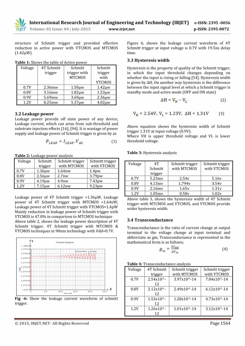
3.2 Leakage power Leakage power provide off state power of any device, Leakage current, which can arise from sub-threshold and substrate injection effects [16], [94]. It is wastage of power supply and leakage power of Schmitt trigger is given by as
(1)
Table 2: Leakage power analysis
Voltage Schmitt trigger
Schmitt trigger with MTCMOS
Schmitt trigger with VTCMOS
0.7V 1.36µw 1.64nw 1.4pw 0.8V 2.56µw 2.7nw 3.79pw 0.9V 4.19µw 4.9nw 7.43pw 1.2V 7.15µw 6.12nw 9.23pw
Leakage power of 4T Schmitt trigger =1.36µW, Leakage power of 4T Schmitt trigger with MTCMOS =1.64nW, Leakage power of 4T Schmitt trigger with VTCMOS=1.4pW Mainly reduction in leakage power of Schmitt trigger with VTCMOS is 47.8% in comparison to MTCMOS technique Above table 2, shows the leakage power description of 4T Schmitt trigger, 4T Schmitt trigger with MTCMOS & VTCMOS techniques in 90nm technology with Vdd=0.7V.
Fig -6: Show the leakage current waveform of schmitt trigger.
Figure 6, shows the leakage current waveform of 4T Schmitt trigger at input voltage is 0.7V with 19.5ns delay time.
3.3 Hysteresis width
Hysteresis is the property of quality of the Schmitt trigger, in which the input threshold changes depending on whether the input is rising or falling [54]. Hysteresis width is given by ∆H, On another way hysteresis is the difference between the input signal level at which a Schmitt trigger is standby mode and active mode (OFF and ON state)
(2)
(3)
Above equation shows the hysteresis width of Schmitt trigger 1.31V at input voltage (0.9V). Where VH is upper threshold voltage and VL is lower threshold voltage.
Table 3: Hysteresis analysis
Above table 3, shows the hysteresis width of 4T Schmitt trigger with MTCMOS and VTCMOS, and VTCMOS provide wider hysteresis width.
3.4 Transconductance
Transconductance is the ratio of current change at output terminal to the voltage change at input terminal and abbreviate as gm, Transconductance is represented in the mathematical form is as follows;
(4)
Table 4: Transconductance analysis
Voltage 4T Schmitt trigger
Schmitt trigger with MTCMOS
Schmitt trigger with VTCMOS
0.7V 2.54x10^-12
3.97x10^-14 7.84x10^-14
0.8V 2.12x10^-12
2.49x10^-14 6.12x10^-14
0.9V 1.53x10^-12
1.28x10^-14 4.73x10^-14
1.2V 1.26x10^-12
1.01x10^-14 3.12x10^-14
Voltage 4T Schmitt trigger
Schmitt trigger with MTCMOS
Schmitt trigger with VTCMOS
0.7V 5.23mv 2.54v 5.16v 0.8V 4.13mv 1.794v 3.54v 0.9V 2.16mv 1.65v 1.31v 1.2V 1.05mv 0.58v 1.02v

International Research Journal of Engineering and Technology (IRJET) e-ISSN: 2395 -0056
Volume: 02 Issue: 04 | July-2015 www.irjet.net p-ISSN: 2395-0072
© 2015, IRJET.NET- All Rights Reserved Page 1565
Fig -7:Show the greph of transconductance of schmitt trigger in Vdd 0.7V.
3.5 DC Response
DC Response is the ratio of o/p voltage to i/p voltage for the circuit.
DC Response= Vout/Vin (5)
DC Response waveform of Schmitt trigger at 0.7v supply voltage is at input Mi (6.163V, 6.163V) and o/p Mo (5.39V, 1.55V).
Fig -8: Show the greph of DC response.
Above figure 8 shows input-output DC response waveform of 4T Schmitt trigger in 90nm technology with Vdd = 0.7V.
3.6 Efficiency
Efficiency is providing the capacity of any circuit. High efficiency means fewer power drains and the input supply and fewer temperature buildups, allowing for small lighter power supplies and structure enclosures. Efficiency is meanly measured as
Efficiency= (output value/input value)*100 (6)
Efficiency using MTCMOS technique =63.06% (7)
Efficiency using VTCMOS technique = 76.84% (8)
Fig -9: Effeciency factor in Schmitt trigger with MTCMOS
Figure 9 shows the duty cycle of Schmitt trigger with MTCMOS and figure 11 is shows the efficiency of Schmitt trigger with VTCMOS when the input voltage rises from 0.7V to 1.2V.
Fig -10: Effciency in schmitt trigger with VTCMOS
4. SUMMARY
Schmitt trigger have been simulated on MATLAB spectre tool in 90nm technology with MTCMOS and VTCMOS technique for enhancing the circuit parameter. Schmitt trigger is basically used in oscillator and wave shaping digital & analog communication circuits. In this discussion comparative description of MTCMOS and VTCMOS have been presented on the bases of min leakage power (1.4pW), max hysteresis width (1.31V), transconductance (3.97x10^-14s) and tranresistance (3.075x10^11ohm) at supply voltage Vdd=0.7V and threshold voltage (0.35V). Simulation result provides Schmitt trigger with VTCMOS is better than MTCMOS technique with little propagation delay in (fsec).this type of design is using in low power communication systems.
International Research Journal of Engineering and Technology (IRJET) e-ISSN: 2395 -0056
Volume: 02 Issue: 04 | July-2015 www.irjet.net p-ISSN: 2395-0072
© 2015, IRJET.NET- All Rights Reserved Page 1566
ACKNOWLEDGEMENTS: This work was supported by MITRC, Alwar, with the calibration MATLAB design system Bangalore.
REFERENCE
[1] C. Zhang, A. Srivastava and P. Ajmera, “Low Voltage CMOS Schmitt Trigger Circuit," IEEE Electronics Letters, Vol.39, No.24, pp.1696-1698, nov. 2003.
[2] C. Wu and C. Chiang, “A low Photo Current CMOS Retinal Focal-Plane Sensor with a Pseudo-BJT Smoothing Networking and an Adaptive Current Schmitt Trigger for Scanner Application” ,IEEE Sensors J. Vol.4, No.4, pp. 510-510, August 2004.
[3] H.Morimura, T. Shimannura, K. Fujii, S. Shigematsu, Y. Okazaki and M. Katsuyuki, “A zero sink current Schmitt trigger and window flexible counting circuit for fingerprint sensors/identifier” IEEE International Solid State Circuit Conference (ISSCC), Vol.1, pp.122-517, 2004.
[4] S.L.Chen and K.Ming-Dou, “A new Schmitt trigger circuit in a 0.13µ 1/2.5v CMOS processes to receive 3. 3v input signals," IEEE Transaction on Circuits and System 2; Express Briefs, Vol.52, issue 7. pp. 361-365, 2005.
[5] V. Pedroni, “LOW-Voltage high speed Schmitt trigger and compact window comparator," IEEE Electronics Letter, Vol.41, no.22, 1213-1214, 2005.
[6] H. Kim, H.J.Kim and W.S.Chung, “Pulse width modulator circuit using CMOS Oats," IEEE Transactions on Circuit and System 1; Regular papers, Vol.54, pp.1869-1878, sept. 2007.
[7] C. Kho Pham “CMOS Schmitt Trigger Circuit with controllable hysteresis using logical threshold voltage control circuit” IEEE Vol.36, No.1821-1824, 2007.
[8] Kulkarni, K. Kim, and K. Roy, “A 160mV robust Schmitt trigger based sub-threshold SRAM," IEEE J. Solid State Circuits, Vol.42, NO. 10, pp. 2303-2313, October 2007.
[9] Jay deep P. Kulkarni, Keejong Kim, and Kaushilc, “A 160mV robust Schmitt trigger based sub-threshold SRAM," IEEE Journal of the solid-state circuit. Vol.42, No. 171-176, Oct 2007.
[10] V.Katyal, R. L. Geiger and D. J. Chen,“Adjustable Hysteresis CMOS Schmitt Trigger," IEEE ISCAS, pp.1938-1941, 2008.
[11] Yoichi Sasaki, Kazuteru Nanba and Hideo Ito, “Circuit and latch capable of masking soft error with Schmitt trigger," Journal of Electronic Testing Vol. 24, No. 1-3 2008.
[12] Sungsik Lee, Ahra Lee, Chang Han Je, Myung Lee, Gunn Hwang and Chang-Auck Choi”1.5v sub mw cmos interfaces circuit for capacitive sensor application in ubiquitous sensor networks”ETRI Journal, viol.30, No.5, oct. 2008.
[13] S.Saini, S. Veeramachaneni, A. M. Kumar, M.B. Srinivas, M.B., “Schmitt trigger as an alternative to buffer insertion for delay and power reduction in VLSI interconnects," TENCON 2009-2009 IEEE Region 10 conferences, pp. 1-5, 2009.
[14] F.Yuan, “A high-speed differential CMOS Schmitt trigger with regenerative current feedback and adjustable hysteresis," Analog Integrated Circuit and Signal Processing, Vol.63, No.1, pp.121-127, 2010.
[15] F. Yuan, “Differential CMOS Schmitt trigger with tunable hysteresis," Analog Integrated Circuit and Signal Processing, Vol.62, No.2, pp.290-248, 2010.
[16] Avireni Srinivasulu,“A Novel current Conveyon based Schmitt trigger and its application as a relaxation oscillator” Vol.39, No. 678-686. Issue6. 29 ARP 2010.
[17] Zafer Takhirav, Bobak Nazer, and Ajay Jashi, “Error mitigation in digital logic using a feedback equalization with Schmitt trigger (FEST) circuit” IEEE, Vol.22, No. 321-327, 2011.
[18] Pratchayaporn Singhanath Varakorn Kasemsuwant and kittipal Chitsakul, “DTMOS Schmitt Trigger with fully adjustable hysteresis” IPCSIT Vol.7 (2011).
[19] Shrivathsava N.L., Tripathi and Kulkarni, “Novel design of VCO with output peak to peak at control”, (IJICA), ISSN; 2231-1890 Vol.1 Issue 2, 2011
[20] R. Rohith Kumar Reddy, N Ramanjaneyule, “high performance CMOS Schmitt Trigger” Vol.2 Issue, July- August 2012, pp.23, 1-2324.
[21] Aaron Arthurs, Justin Roork, and jiadi, “A Comparative study of ultra-low voltage digital circuit design," International Solid State Circuit Conference (ISSCC) 2012.
[22] Swati Kundra, Priyanka Soni. “Low power Schmitt Trigger” ISSN 2222-1727 Vol.3, No.2, 2012.
[23] Shikha Singh, V. Sclochana Verma, “Crasstalk noise and delay reduction in VLSI interconnects," ISSN No. 2250-3536.Vol.2 ISSUE 2, March 2012.
[24] Archana nagda, Rajendra's Prasad, N.K. Vyas, “Leakage power reduction techniques; A new approach," ISSN 2248-9622, Vol.2 Issue 2, mar-apr 2012, pp. 308-312.
[25] Yogeshwar Singh Randhawa and Sanjay Sharma, “Effect of Multi Threshold Techniques on Compretive Study of 11T and 6T Cell during Leakage Power Robustness”, Quantum Matter, ISSN; 2164-7515, Vol. 2, pp. 105-108, Issue 2013.
[26] Tuzun, Burcu, Erkoc, “Structural and Electronic Properties of Unusual Carbon Nanorods”, Quantum Matter, ISSN; 2164-7515, Vol. 1, No 2 pp. 136-148, December 2012.
[27] Paitya, N. Bhattacharya, S. and Ghatak, “Influence of Quantizing Magnetic Field on the Fowler-Nordheim Field Emission form Non-Parabolic Materials”, Quantum Matter, ISSN; 2164-7515, Vol. 1, No 1, pp. 63-85, June 2012.
Related Documents