International Research Journal of Engineering and Technology (IRJET) e-ISSN: 2395-0056 Volume: 02 Issue: 03 | Jun e-2015 www.irjet.net p-ISSN: 2395-0072 © 2015, IRJET.NET- All Rights Reserved Page 385 NANOCAVITY BASED OPTICAL PRESSURE SENSOR Mohankumar B S 1 , Mrs.Indira Bahaddur 2 1 MTech (DECS), Dept. of E&C, Malnad College of Engineering Hassan, Karnataka, India 2 Asst.Professor, Dept. of E&C, Malnad College of Engineerin g Hassan, Karnataka, Ind ia Abstract -In this paper, we design and simulation photonic crystal (Phc) Nano press ure senso r. The senso r is made of two dimensional photonic crystal and consists of hexagonal lattice structure. Photonic c rystal structure uses an line defect engineering to create an waveguide. The Nano cavity is f ormed by changing the radius of a single rod in air structure, which is at the centre of lattice. This sensor supports 1450-1550nm wavelength. Simulation results show that resonant frequency of Nano cavity changed with the increased pressure. Key words: photonic crystal; waveguide; Nano cavity; pressure sensor, Nano-pressure. 1 INTRODUCTION Photonic crystals are periodic microstructure or nano structure affected by the propagation of photon. Based on the geometry of the structure photonic crystal can be classified into one dimensional (1D) two dimensional (2D), three dimensional (3D) structure [4]. PhC have photonic band gap (PBG) manipulates beam of light. Photon travels in these structures with a different wavelength. For the design 2D photonic crystal is used in 2D crystal the permittivity is changed in two directions. Defects can be done either by changing the dimension or removal from the structure and acts as a resonant cavity. Defects modify and control the flow of light i nside the photonic crystal [8]. An example of application of photonic crystals is bio sensors, mechanical parameter sensor like pressure, nano displacement, structural health monitoring, chemical sensors and acoustic sensors. In this paper, we modulate and simulate a Nano pressure sensor with two dimensional photonic crystal Nano cavity resonators. The finite difference time domain (FDTD) method is used to simulate sensor operation for different pressur e. When th e pressure is applied stress is distributed over the crystal structure and the refractive index is changed. The pressure can be calculated using P = Aωρ0C P= acoustic pressure A=displacement amplitude ω= 2πf ρ0= specific density of medium C= speed of sound under water Thus pressure is proportional to displacement. 2 DESIGN In this paper uses the two dimensional photonic crystal. First design a hexagonal lattice structure. Line defect engineering isintroducedby removing the rods in hair structure. To create a resonant cavityplace a singlerod in the middle of the lattice with a n increased radius and place the neighbouring coordinates with another radius. Introduce the lightsource in one end ofthewave guide and lightis obtained at the detector. When the pressure is zero, displacement is also zero.The pressureis applied on the resonant cavity the propagationof lightthrough the hexagonal latticechanged and refractive index also changed. MEEP is the tool used for design and simulation of a photonic crystal. MEEP stands for MIT electromagnetic equation propagation. It is used in solving of Maxwell’s equations in periodic dielectric structure simulation in 1D, 2D, 3D and cylindrical coordinates can be done. The transmitter flux can be obtained at each frequency (ω). This is the integrals of the pointing vector over a plane of the photonic crustal structure [14]. The time domain applications of MEEP consist of transmission and reflection spectra, resonant mode& frequencies and field patterns. The finite-difference time- domain (FDTD) method is used to simulate operation of sensors in different pressures. MEEP is the tool where we design and simulation of the photonic crystal and parameters are given below. 1) Rods in air configuration 2) Hexagonal lattice structure

IRJET-NANOCAVITY BASED OPTICAL PRESSURE SENSOR
Jan 14, 2016
In this paper, we design and simulation photonic crystal (Phc) Nano pressure sensor. The sensor is made of two dimensional photonic crystal and consists of hexagonal lattice structure. Photonic crystal structure uses an line defect engineering to create an waveguide. The Nano cavity is formed by changing the radius of a single rod in air structure, which is at the centre of lattice. This sensor supports 1450-1550nm wavelength. Simulation results show that resonant frequency of Nano cavity changed with the increased pressure.
Welcome message from author
This document is posted to help you gain knowledge. Please leave a comment to let me know what you think about it! Share it to your friends and learn new things together.
Transcript
7/18/2019 IRJET-NANOCAVITY BASED OPTICAL PRESSURE SENSOR
http://slidepdf.com/reader/full/irjet-nanocavity-based-optical-pressure-sensor 1/5
International Research Journal of Engineering and Technology (IRJET) e-ISSN: 2395-0056
Volume: 02 Issue: 03 | June-2015 www.irjet.net p-ISSN: 2395-0072
© 2015, IRJET.NET- All Rights Reserved Page 385
NANOCAVITY BASED OPTICAL PRESSURE SENSOR
Mohankumar B S1, Mrs.Indira Bahaddur2
1MTech (DECS), Dept. of E&C, Malnad College of Engineering Hassan, Karnataka, India 2 Asst.Professor, Dept. of E&C, Malnad College of Engineering Hassan, Karnataka, India
Abstract -In this paper, we design and simulation
photonic crystal (Phc) Nano pressure sensor. The sensor
is made of two dimensional photonic crystal and
consists of hexagonal lattice structure. Photonic crystal
structure uses an line defect engineering to create an
waveguide. The Nano cavity is formed by changing the
radius of a single rod in air structure, which is at the
centre of lattice. This sensor supports 1450-1550nm
wavelength. Simulation results show that resonant
frequency of Nano cavity changed with the increased
pressure.
Key words: photonic crystal; waveguide; Nano cavity;
pressure sensor, Nano-pressure.
1 INTRODUCTION
Photonic crystals are periodic microstructure or nano
structure affected by the propagation of photon. Based onthe geometry of the structure photonic crystal can be
classified into one dimensional (1D) two dimensional (2D),
three dimensional (3D) structure [4]. PhC have photonic
band gap (PBG) manipulates beam of light. Photon travels
in these structures with a different wavelength. For the
design 2D photonic crystal is used in 2D crystal the
permittivity is changed in two directions. Defects can be
done either by changing the dimension or removal from
the structure and acts as a resonant cavity. Defects modify
and control the flow of light inside the photonic crystal [8].
An example of application of photonic crystals is bio
sensors, mechanical parameter sensor like pressure, nano
displacement, structural health monitoring, chemical
sensors and acoustic sensors.
In this paper, we modulate and simulate a Nano pressure
sensor with two dimensional photonic crystal Nano cavity
resonators. The finite difference time domain (FDTD)
method is used to simulate sensor operation for different
pressure. When the pressure is applied stress is distributed
over the crystal structure and the refractive index is
changed.
The pressure can be calculated using
P = Aωρ0C P= acoustic pressure
A=displacement amplitude
ω= 2πf
ρ0= specific density of medium
C= speed of sound under water
Thus pressure is proportional to displacement.
2 DESIGN
In this paper uses the two dimensional photonic crystal.
First design a hexagonal lattice structure. Line defect
engineering isintroducedby removing the rods in hair
structure. To create a resonant cavityplace a singlerod in
the middle of the lattice with an increased radius and place
the neighbouring coordinates with another radius.
Introduce the lightsource in one end ofthewave guide and
lightis obtained at the detector.
When the pressure is zero, displacement is also zero.The
pressureis applied on the resonant cavity the
propagationof lightthrough the hexagonal latticechangedand refractive index also changed.
MEEP is the tool used for design and simulation of a
photonic crystal. MEEP stands for MIT electromagnetic
equation propagation. It is used in solving of Maxwell’s
equations in periodic dielectric structure simulation in 1D,
2D, 3D and cylindrical coordinates can be done. The
transmitter flux can be obtained at each frequency (ω).
This is the integrals of the pointing vector over a plane of
the photonic crustal structure [14].
The time domain applications of MEEP consist of
transmission and reflection spectra, resonant mode&
frequencies and field patterns. The finite-difference time-
domain (FDTD) method is used to simulate operation of
sensors in different pressures.
MEEP is the tool where we design and simulation of the
photonic crystal and parameters are given below.
1) Rods in air configuration
2) Hexagonal lattice structure
7/18/2019 IRJET-NANOCAVITY BASED OPTICAL PRESSURE SENSOR
http://slidepdf.com/reader/full/irjet-nanocavity-based-optical-pressure-sensor 2/5
International Research Journal of Engineering and Technology (IRJET) e-ISSN: 2395-0056
Volume: 02 Issue: 03 | June-2015 www.irjet.net p-ISSN: 2395-0072
© 2015, IRJET.NET- All Rights Reserved Page 386
3) Lattice constant ‘a’ = 1nm
4) Radius of the rod ‘r’ = 0.19nm
5) Height of the slab is infinity
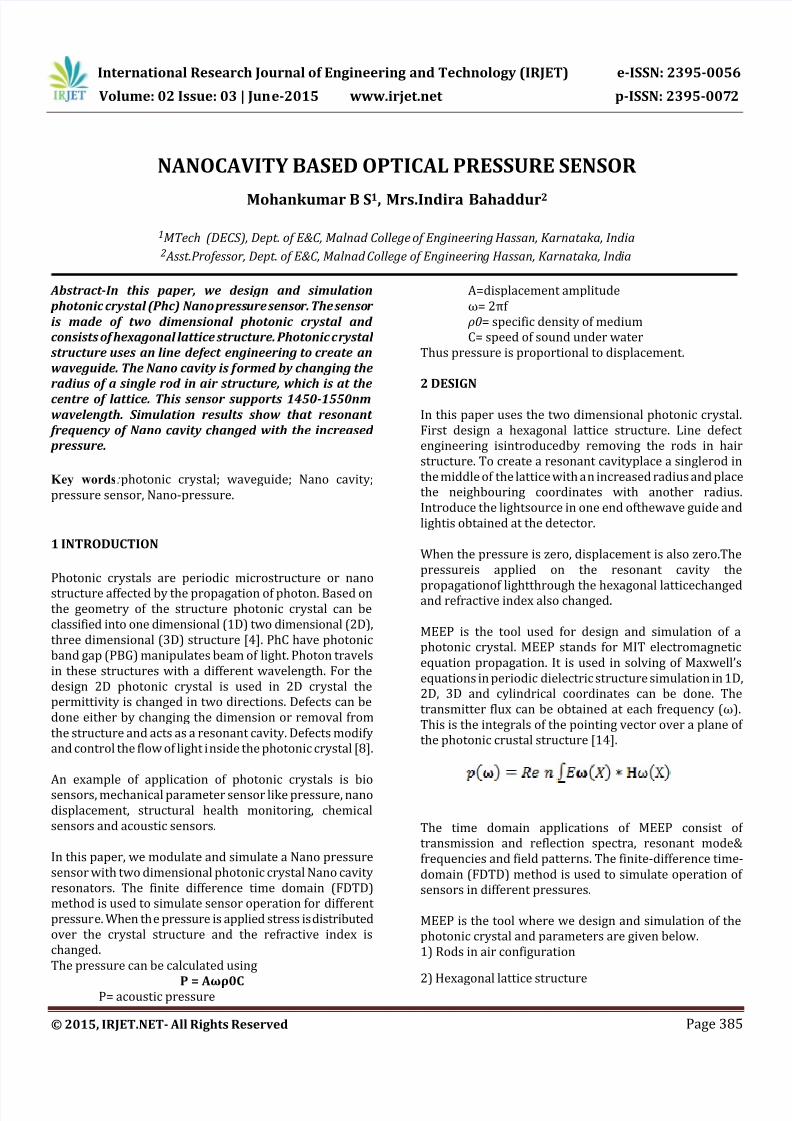
Fig-1: Layout of PhC structure consists of hexagonal lattice
Fig 2: The layout of sensor structure consists of line
defect waveguide directed couple to Nano cavity.
waveguide directly connected to the Nanocavity. The light
enters from the left of waveguide. A photo detectorin the
end of waveguide detects the light.
When the pressure is applied on the dielectric slab
displacement takes place so that the nature of the
electromagnetic waves is altered.
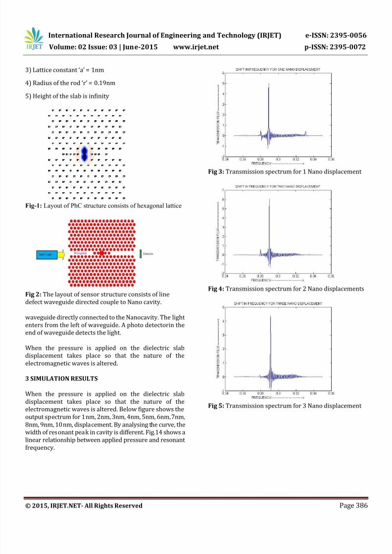
3 SIMULATION RESULTS
When the pressure is applied on the dielectric slab
displacement takes place so that the nature of the
electromagnetic waves is altered. Below figure shows the
output spectrum for 1nm, 2nm, 3nm, 4nm, 5nm, 6nm, 7nm,
8nm, 9nm, 10nm, displacement. By analysing the curve, the
width of resonant peak in cavity is different. Fig.14 shows a
linear relationship between applied pressure and resonant
frequency.
Fig 3: Transmission spectrum for 1 Nano displacement
Fig 4: Transmission spectrum for 2 Nano displacements
Fig 5: Transmission spectrum for 3 Nano displacement
7/18/2019 IRJET-NANOCAVITY BASED OPTICAL PRESSURE SENSOR
http://slidepdf.com/reader/full/irjet-nanocavity-based-optical-pressure-sensor 3/5
International Research Journal of Engineering and Technology (IRJET) e-ISSN: 2395-0056
Volume: 02 Issue: 03 | June-2015 www.irjet.net p-ISSN: 2395-0072
© 2015, IRJET.NET- All Rights Reserved Page 387
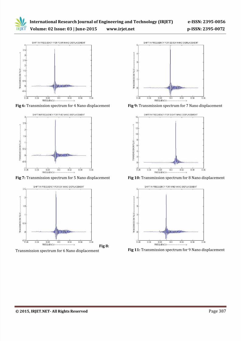
Fig 6: Transmission spectrum for 4 Nano displacement
Fig 7: Transmission spectrum for 5 Nano displacement
Fig 8:
Transmission spectrum for 6 Nano displacement
Fig 9: Transmission spectrum for 7 Nano displacement
Fig 10: Transmission spectrum for 8 Nano displacement
Fig 11: Transmission spectrum for 9 Nano displacement
7/18/2019 IRJET-NANOCAVITY BASED OPTICAL PRESSURE SENSOR
http://slidepdf.com/reader/full/irjet-nanocavity-based-optical-pressure-sensor 4/5
International Research Journal of Engineering and Technology (IRJET) e-ISSN: 2395-0056
Volume: 02 Issue: 03 | June-2015 www.irjet.net p-ISSN: 2395-0072
© 2015, IRJET.NET- All Rights Reserved Page 388
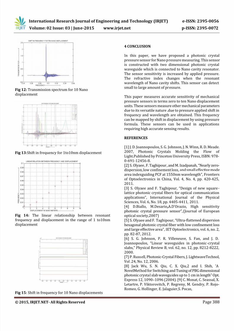
Fig 12: Transmission spectrum for 10 Nano
displacement
Fig 13:Shift in frequency for 1to10nm displacement
Fig 14: The linear relationship between resonant
frequency and displacement in the range of 1 to10nm
displacement
Fig 15: Shift in frequency for 10 Nano displacements
4 CONCLUSION
In this paper, we have proposed a photonic crystal
pressure sensor for Nano pressure measuring. This sensor
is constructed with two dimensional photonic crystal
waveguide which is connected to Nano cavity resonator.
The sensor sensitivity is increased by applied pressure.
The refractive index changes when the resonant
wavelength of Nano cavity shifts. This sensor can detect
small to large amount of pressure.
This paper measures accurate sensitivity of mechanical
pressure sensors in terms zero to ten Nano displacement
units. These sensors measure other mechanical parameters
due to its versatile nature .due to pressure applied shift in
frequency and wavelength are obtained. This frequencycan be mapped by shift in displacement by using pressure
formula. These sensors can be used in applications
requiring high accurate sensing results.
REFERENCES
[1] J. D. Joannopoulos, S. G. Johnson, J. N. Winn, R. D. Meade.
2007, Photonic Crystals Molding the Flow of
Light.Published by Princeton University Press, ISBN: 978-
0-691-12456-8.
[2] S. Olyaee, F. Taghipour, and M. Izadpanah, “Nearly zero-
dispersion, low confinement loss, and small effective mode
area indexguiding PCF at 1550nm wavelength”, Frontiersof Optoelectronics in China, Vol. 4, No. 4, pp. 420-425,
2011.
[3] S. Olyaee and F. Taghipour, “Design of new square-
lattice photonic crystal fibers for optical communication
applications”, International Journal of the Physical
Sciences, Vol. 6, No. 18, pp. 4405-4411, 2011.
[4] D.Biallo, M.Desario,A.D’Orazio, High sensitivity
photonic crystal pressure sensor”,(Journal of European
optical society,2007)
[5] S. Olyaee and F. Taghipour, “Ultra-flattened dispersion
hexagonal photonic crystal fiber with low confinement loss
and large effective area”, IET Optoelectronics, vol. 6, no. 2,
pp. 82-87, 2012.
[6] S. G. Johnson, P. R. Villeneuve, S. Fan, and J. D.
Joannopoulos, “Linear waveguides in photonic-crystal
slabs,” Physical Review B, vol. 62, no. 12, pp. 8212-8222,
2000.
[7] P. Russell, Photonic-Crystal Fibers, J. LightwaveTechnol,
Vol .24, No. 12, 2006.
[8] Jack Wu, S. N. Qiu, C. X. Qiu,2 and I. Shih, 'A
NovelMethod for Switching and Tuning of PBG dimensional
photonic crystal slab waveguides up to 1 cm in length” Opt.
Express 12, 1090–1096 (2004). [9] C. Monat, C. Seassal, X.
Letartre, P. Viktorovitch, P. Regreny, M. Gendry, P. Rojo-
Romeo, G. Hollinger, E. Jalaguier,S. Pocas,
7/18/2019 IRJET-NANOCAVITY BASED OPTICAL PRESSURE SENSOR
http://slidepdf.com/reader/full/irjet-nanocavity-based-optical-pressure-sensor 5/5
International Research Journal of Engineering and Technology (IRJET) e-ISSN: 2395-0056
Volume: 02 Issue: 03 | June-2015 www.irjet.net p-ISSN: 2395-0072
© 2015, IRJET.NET- All Rights Reserved Page 389
and B. Aspar, ‘‘InP 2D photonic crystal microlaser on Si
wafer: room temperature operation at 1.55mm,’’ Electron.
Lett.37, 764–765, 2001.
[10] M. Fatih and Y. Fan, “High-contrast all-optical bistable
switching in photonic crystal microcavities,” Appl. Phys.
Lett., Vol. 83, No. 14, p. 6, 2003.
[11] S. Olyaee and A. A. Dehghani, “High resolution and
wide dynamic range pressure sensor based on two-
dimensional photonic crystal”, Photonic Sensors, Vol. 2, No.
1, pp. 92-96, 2012
[12] J. Shi, V.S. Hsiao, T. R. Walker, T. J. Huang, “Humidity
sensing based on Nanoporous polymeric photonic
crystals,” Sensors and Actuators B, Vol. 129, pp. 391–396,
2008.
[13] R. V. Nair, R.Vijaya, Photonic crystal sensors, Vol. 34,
Issue 3, May 2010, pp. 89-134.
[14] I. EI-Kady,M.M. R. Taha, and M. F. Su, “Application ofphotonic crystals in submicron damage detection and
quantification,” Appl. Phys. Lett., vol. 88, pp. 253109–
253109, 2006.
BIOGRAPHIES
MOHAN KUMAR B S, PG Student,
Department of E&C Engineering,MCE Hassan, VTU Belgavi,
Karnataka, India.
E-mail:
INDIRA BAHADDUR, Assistant
Professor, Department of E&C
Engineering, MCE Hassan, VTU
Belgavi, Karnataka, India.
E-mail: [email protected]
Related Documents