DS615 March 1, 2011 www.xilinx.com 1 Product Specification © Copyright 2008 - 2009, 2011 Xilinx, Inc. XILINX, the Xilinx logo, Kintex, Virtex, Spartan, ISE and other designated brands included herein are trademarks of Xilinx in the United States and other countries. MATLAB and Simulink are registered trademarks of The MathWorks, Inc. All other trademarks are the property of their respective owners. Introduction The Xilinx LogiCORE™ IP Discrete Fourier Transform (DFT) core meets the requirements for 3GPP Long Term Evolution (LTE) [Ref 1] systems. The point size of the transformation (N) can be speci- fied on a frame-by-frame basis and can take the values N=2 M *3 P *5 Q , where M, P, and Q can be set to a range of values (as in Table 2) that meet the LTE system require- ments. Features • Drop-in module for Kintex ™-7, Virtex ® -7, Virtex ® -6, Virtex-5, Virtex-4, Spartan ® -6 and Spartan-3A DSP FPGAs • Support for wide range of transform sizes • Less than 26 μ s total latency when transforming 1200 points at 245.76 MHz (using any combination of sizes) • Size can be changed for each transform • New point sizes 1296 and 1536 added • Up to 18-bit two’s complement input data width, up to 18-bit two’s complement output data width with 4-bit block exponent • Direct and inverse DFT supported on frame-by-frame basis IP LogiCORE Discrete Fourier Transform v3.1 DS615 March 1, 2011 Product Specification LogiCORE IP Facts Table Core Specifics Supported Device Family (1) 1. For a complete listing of supported devices, see the release notes for this core. Virtex-7 and Kintex-7, Virtex-6, Virtex-5, Virtex-4, Spartan-6, Spartan-3A DSP Supported User Interfaces Not Applicable Provided with Core Documentation Product Specification Design Files Netlist Example Design Not Provided Test Bench Not Provided Constraints File Not Applicable Simulation Model VHDL behavioral model in the xilinxcorelib library VHDL UniSim structural model Verilog UniSim structural model Tested Design Tools Design Entry Tools CORE Generator tool 13.1 Simulation Mentor Graphics ModelSim 6.6d Cadence Incisive Enterprise Simulator (IES) 10.2 Synopsys VCS and VCS MX 2010.06 ISIM 13.1 Synthesis Tools N/A Support Provided by Xilinx, Inc.

Welcome message from author
This document is posted to help you gain knowledge. Please leave a comment to let me know what you think about it! Share it to your friends and learn new things together.
Transcript
DS615 March 1, 2011 www.xilinx.com 1Product Specification
© Copyright 2008 - 2009, 2011 Xilinx, Inc. XILINX, the Xilinx logo, Kintex, Virtex, Spartan, ISE and other designated brands included herein are trademarks of Xilinx in the United States and other countries. MATLAB and Simulink are registered trademarks of The MathWorks, Inc. All other trademarks are the property of their respective owners.
IntroductionThe Xilinx LogiCORE™ IP Discrete Fourier Transform(DFT) core meets the requirements for 3GPP Long TermEvolution (LTE) [Ref 1] systems.
The point size of the transformation (N) can be speci-fied on a frame-by-frame basis and can take the valuesN=2M*3P*5Q, where M, P, and Q can be set to a range ofvalues (as in Table 2) that meet the LTE system require-ments.
Features• Drop-in module for Kintex™-7, Virtex®-7, Virtex®-6,
Virtex-5, Virtex-4, Spartan®-6 and Spartan-3A DSP FPGAs
• Support for wide range of transform sizes
• Less than 26 μs total latency when transforming 1200 points at 245.76 MHz (using any combination of sizes)
• Size can be changed for each transform
• New point sizes 1296 and 1536 added
• Up to 18-bit two’s complement input data width, up to 18-bit two’s complement output data width with 4-bit block exponent
• Direct and inverse DFT supported on frame-by-frame basis
IP LogiCOREDiscrete Fourier Transform v3.1
DS615 March 1, 2011 Product Specification
LogiCORE IP Facts Table
Core Specifics
Supported Device Family(1)
1. For a complete listing of supported devices, see the release notesfor this core.
Virtex-7 and Kintex-7,Virtex-6, Virtex-5, Virtex-4,
Spartan-6, Spartan-3A DSP
Supported User Interfaces Not Applicable
Provided with Core
Documentation Product Specification
Design Files Netlist
Example Design Not Provided
Test Bench Not Provided
Constraints File Not Applicable
Simulation Model
VHDL behavioral model in the xilinxcorelib libraryVHDL UniSim structural model
Verilog UniSim structural model
Tested Design Tools
Design Entry Tools CORE Generator tool 13.1
Simulation
Mentor Graphics ModelSim 6.6dCadence Incisive Enterprise Simulator (IES) 10.2
Synopsys VCS and VCS MX 2010.06ISIM 13.1
Synthesis Tools N/A
Support
Provided by Xilinx, Inc.
DS615 March 1, 2011 www.xilinx.com 2Product Specification
IP LogiCORE Discrete Fourier Transform v3.1
OverviewThe DFT design has a fully synchronous interface. Figure 1 shows the pin-out of the design. See Table 1 for moredetails on ports.
The core indicates that it is ready to accept a new frame of data by setting RFFD high. When RFFD is high, data inputmay be started by setting FD_IN high for one or more cycles. Data is input via XN_RE and XN_IM. It should be pro-vided over N cycles without interruption. Data input and output are complex and in natural order. FD_OUT signalswhen the core starts data output and DATA_VALID signals when data on XK_RE and XK_IM is valid.
Note that FD_IN is ignored while RFFD is low, and so FD_IN can be kept high for multiple cycles. FD_IN is acceptedon the first cycle that RFFD is high.
If FD_IN is set permanently high, then the core will start a new frame of data input as soon as the core is ready. Thisarrangement provides maximum transform throughput. Alternatively, RFFD may be connected directly to FD_INto achieve the same behavior.
The first element of input data should be provided on the same cycle that the core starts to receive data, that is, thefirst cycle in which both FD_IN and RFFD are high.
PinoutThe pin-out of the DFT is summarized in Table 1.
X-Ref Target - Figure 1
Figure 1: Interface Diagram
Table 1: Pinout
Name Width Direction Description
XN_RE N (1) INPUT Real Data Input: Provide in two's complement fixed-point format. Provide in natural order.
XN_IM N (1) INPUT Imaginary Data Input: Provide in two's complement fixed-point format. Provide in natural order.
FD_IN 1 INPUT First Data In: Set high to indicate start of data input frame. FD_IN is ignored when RFFD is low.
RFFD 1 OUTPUT Ready For First Data: High when the core is ready for a new frame of data. Goes low one cycle after a valid FD_IN.
SIZE 6 INPUT Size In: Size of transform to be performed. Sampled when FD_IN is high (that is, at start of data frame).
FORWARD 1 INPUT Forward: Set high to perform forward transform or low for inverse transform. Sampled when FD_IN is high (that is, at start of data frame).
Intermediate buffer
DFT Engine FORWARD
SIZEXN_RE
FD_INRFFD
CLKSCLR
DATA_VALID
FD_OUT
CE
ds615_01_012308
Dat
a
Con
trol
Dat
a
Con
trol
XN_IMXK_REXK_IM
DS615 March 1, 2011 www.xilinx.com 3Product Specification
IP LogiCORE Discrete Fourier Transform v3.1
FunctionThe forward DFT output is related to the input by the following equation:
where and the input, , is a complex quantity in which and are two’scomplement fixed-point numbers whose values are given by:
where is the t-th bit of .
The output is a complex block floating-point quantity whose value is given by:
where and are two’s complement numbers as defined previously, and the block exponent, , is anunsigned integer with weighted binary representation:
where is the t-th bit of . The block exponent is constant for all elements of a particular DFT output frame.
SCLR 1 INPUT Synchronous Clear: Set high for a single cycle to reset the core. This must be performed after power-on. If the core is processing data at the time a reset is performed, then processing is halted immediately and any intermediate data is discarded. After reset the core is ready to accept new input frames.
CLK 1 INPUT Clock
CE 1 INPUT Clock Enable: Clock enable has lower precedence than SCLR
XK_RE N(1) OUTPUT Real Data Output: Provided in natural order and in fixed-point format.
XK_IM N(1) OUTPUT Imaginary Data Output: Provided in natural order and in fixed-point format.
BLK_EXP 4 OUTPUT Block exponent: Provided as unsigned integer.
FD_OUT 1 OUTPUT First Data Out: Set high by core to indicate that the core is ready to output data.
DATA_VALID 1 OUTPUT Data Valid: Set high by core to indicate that data output is valid.
Notes: 1. N is number of bits per single value, real or imaginary.
Table 1: Pinout (Cont’d)
Name Width Direction Description
X k( ) x n( )e
j2πnk–N
------------------
n 0=
N 1–
∑= k 0 … N 1–, ,=
j 1–= x n( ) xr n( ) jxi n( )+ xr n( ) xi n( )
x x17– xt217– t+
t 0=
16
∑+=
xt x
X k( )
Xr k( ) jXi k( )+( )2b
Xr k( ) Xi k( ) b
b bt2t
t 0=
3
∑=
bt b
DS615 March 1, 2011 www.xilinx.com 4Product Specification
IP LogiCORE Discrete Fourier Transform v3.1
The inverse DFT has the following relationship between input and output:
Again, the input is represented as a complex two’s complement fixed-point value, and the output a complex blockfloating-point value, as defined for the forward transform.
Note that neither the forward nor inverse DFT provides scaling by 1/N.
Format of Input/Output Data
For all bit widths, the fixed point is to the right of the MSB, that is, such that data 'x' takes the range -1.0 ≤ x <1.0. Forbest numerical performance two’s complement input data, that is, less than 18-bits should be zero padded in theleast significant bit positions.
Block exponent (BLK_EXP) is the power of 2 in the block floating point representation for the output data. Its rangeis from 0 to 15.
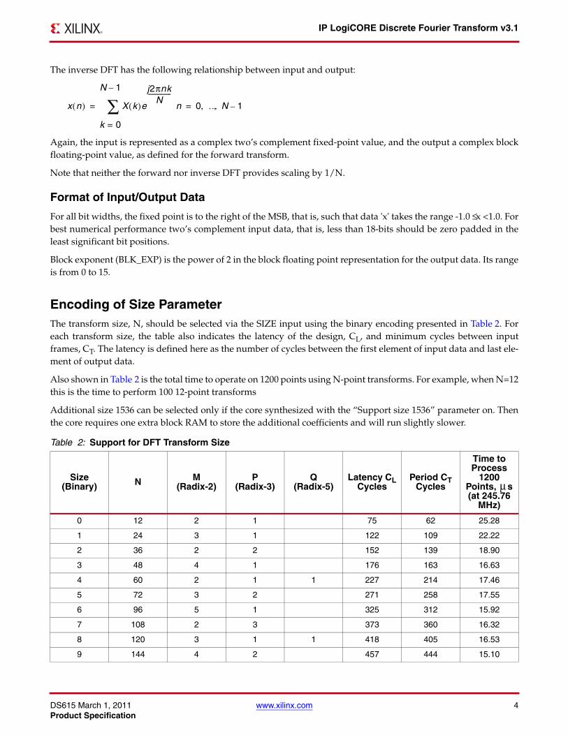
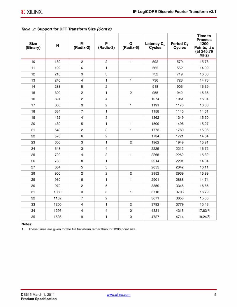
Encoding of Size ParameterThe transform size, N, should be selected via the SIZE input using the binary encoding presented in Table 2. Foreach transform size, the table also indicates the latency of the design, CL, and minimum cycles between inputframes, CT. The latency is defined here as the number of cycles between the first element of input data and last ele-ment of output data.
Also shown in Table 2 is the total time to operate on 1200 points using N-point transforms. For example, when N=12this is the time to perform 100 12-point transforms
Additional size 1536 can be selected only if the core synthesized with the “Support size 1536” parameter on. Thenthe core requires one extra block RAM to store the additional coefficients and will run slightly slower.
Table 2: Support for DFT Transform Size
Size (Binary) N M
(Radix-2)P
(Radix-3)Q
(Radix-5)Latency CL
CyclesPeriod CT
Cycles
Time to Process
1200 Points, s (at 245.76
MHz)
0 12 2 1 75 62 25.28
1 24 3 1 122 109 22.22
2 36 2 2 152 139 18.90
3 48 4 1 176 163 16.63
4 60 2 1 1 227 214 17.46
5 72 3 2 271 258 17.55
6 96 5 1 325 312 15.92
7 108 2 3 373 360 16.32
8 120 3 1 1 418 405 16.53
9 144 4 2 457 444 15.10
x n( ) X k( )e
j2πnkN
---------------
k 0=
N 1–
∑= n 0 … N 1–, ,=
μ
DS615 March 1, 2011 www.xilinx.com 5Product Specification
IP LogiCORE Discrete Fourier Transform v3.1
10 180 2 2 1 592 579 15.76
11 192 6 1 565 552 14.09
12 216 3 3 732 719 16.30
13 240 4 1 1 736 723 14.76
14 288 5 2 918 905 15.39
15 300 2 1 2 955 942 15.38
16 324 2 4 1074 1061 16.04
17 360 3 2 1 1191 1178 16.03
18 384 7 1 1158 1145 14.61
19 432 4 3 1362 1349 15.30
20 480 5 1 1 1509 1496 15.27
21 540 2 3 1 1773 1760 15.96
22 576 6 2 1734 1721 14.64
23 600 3 1 2 1962 1949 15.91
24 648 3 4 2225 2212 16.72
25 720 4 2 1 2265 2252 15.32
26 768 8 1 2214 2201 14.04
27 864 5 3 2855 2842 16.11
28 900 2 2 2 2952 2939 15.99
29 960 6 1 1 2901 2888 14.74
30 972 2 5 3359 3346 16.86
31 1080 3 3 1 3716 3703 16.79
32 1152 7 2 3671 3658 15.55
33 1200 4 1 2 3792 3779 15.43
34 1296 4 4 0 4331 4318 17.63(1)
35 1536 9 1 0 4727 4714 19.24(1)
Notes: 1. These times are given for the full transform rather than for 1200 point size.
Table 2: Support for DFT Transform Size (Cont’d)
Size (Binary) N M
(Radix-2)P
(Radix-3)Q
(Radix-5)Latency CL
CyclesPeriod CT
Cycles
Time to Process
1200 Points, s (at 245.76
MHz)
μ
DS615 March 1, 2011 www.xilinx.com 6Product Specification
IP LogiCORE Discrete Fourier Transform v3.1
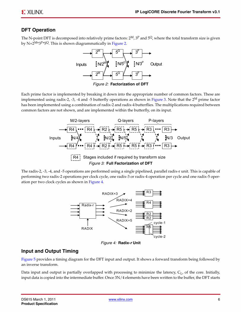
DFT Operation
The N-point DFT is decomposed into relatively prime factors: 2M, 3P and 5Q, where the total transform size is givenby N=2M*3P*5Q. This is shown diagrammatically in Figure 2.
Each prime factor is implemented by breaking it down into the appropriate number of common factors. These areimplemented using radix-2, -3, -4 and -5 butterfly operations as shown in Figure 3. Note that the 2M prime factorhas been implemented using a combination of radix-2 and radix-4 butterflies. The multiplications required betweencommon factors are not shown, and are implemented within the butterfly, on its input.
The radix-2, -3, -4, and -5 operations are performed using a single pipelined, parallel radix-r unit. This is capable ofperforming two radix-2 operations per clock cycle, one radix-3 or radix-4 operation per cycle and one radix-5 oper-ation per two clock cycles as shown in Figure 4.
Input and Output Timing
Figure 5 provides a timing diagram for the DFT input and output. It shows a forward transform being followed byan inverse transform.
Data input and output is partially overlapped with processing to minimize the latency, CL, of the core. Initially,input data is copied into the intermediate buffer. Once 3N/4 elements have been written to the buffer, the DFT starts
X-Ref Target - Figure 2
Figure 2: Factorization of DFT
X-Ref Target - Figure 3
Figure 3: Full Factorization of DFT
X-Ref Target - Figure 4
Figure 4: Radix-r Unit
2M
N/2M
2M
5Q 3P
5Q
N/5Q N/3P
3P
Inputs Output
R4
R4
R2 R3 R3R5
N/4
R4 R5
N/2
R2 R3 R3R5R4 R5
N/3 N/5Inputs Output
M/2-layers P-layers Q-layers
R4 Stages included if required by transform size
Radix-r R4
R3
R2R2
R5cycle-1
cycle-2
RADIX
RADIX=3
RADIX=4
RADIX=2
RADIX=5

DS615 March 1, 2011 www.xilinx.com 7Product Specification
IP LogiCORE Discrete Fourier Transform v3.1
performing the first layer of radix-4 operations (denoted R4 in Figure 5). Subsequent input data is fed directly intothe DFT as each radix-4 operation is performed.
Similarly, data output is overlapped with the last layer of radix-3 operations (denoted R3 in Figure 5), with the firstN/3 samples coming directly from the radix-r unit. The remaining outputs of the radix-r unit are temporarily storedin the intermediate buffer and output over the next 2N/3 cycles.
DFT Throughput
The throughput of the design, measured in terms of the number of DFTs per cycle, is given by 1/CT where CT is thetotal number of cycles between frames of input data. The value of CT for each transform size is summarized inTable 2.
DFT Latency
Single Transform Latency
The minimum latency of the core is defined as the number of cycles from first input to last output. It is summarizedin Table 2.
Multiple Transform Latency
The minimum latency for multiple transforms is obtained by adding the values of CT for each size, and CL for thelast transform. The latency for V transforms of the same size is given by the following equation:
The time to process 1200 points, as summarized in Table 2 and Table 3, has been derived from the preceding equa-tion and the clock period. Note that for point sizes larger than 600, V is given by 1200/N, where N is the point size.The choice of 1200 point as the size is driven by the fact that 1200 point array seems to be the most typical case in theLTE systems.
X-Ref Target - Figure 5
Figure 5: Interface Timing Diagram
S IZ E
F D _ IN
D IN
D A T A _ V A L ID
F D _ O U T
R 4 R 5
P e rio d , C T
N o n -o ve rla p p e d p ro ce ss in g
R 3
F ra m e 1 in F ra m e 2 in
N -p t tra n s fo rm
R F F D
R e se t s ta te
0 N -1
0 1 N -1
0 1 2
D O U T
F O R W A R D
C L K
N -K
L a te n cy , C L
XN_RE & XN_IM
XK_RE & XK_IM
Total Latency V 1–( )CT CL+=
DS615 March 1, 2011 www.xilinx.com 8Product Specification
IP LogiCORE Discrete Fourier Transform v3.1
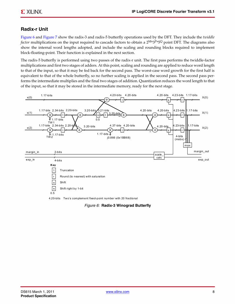
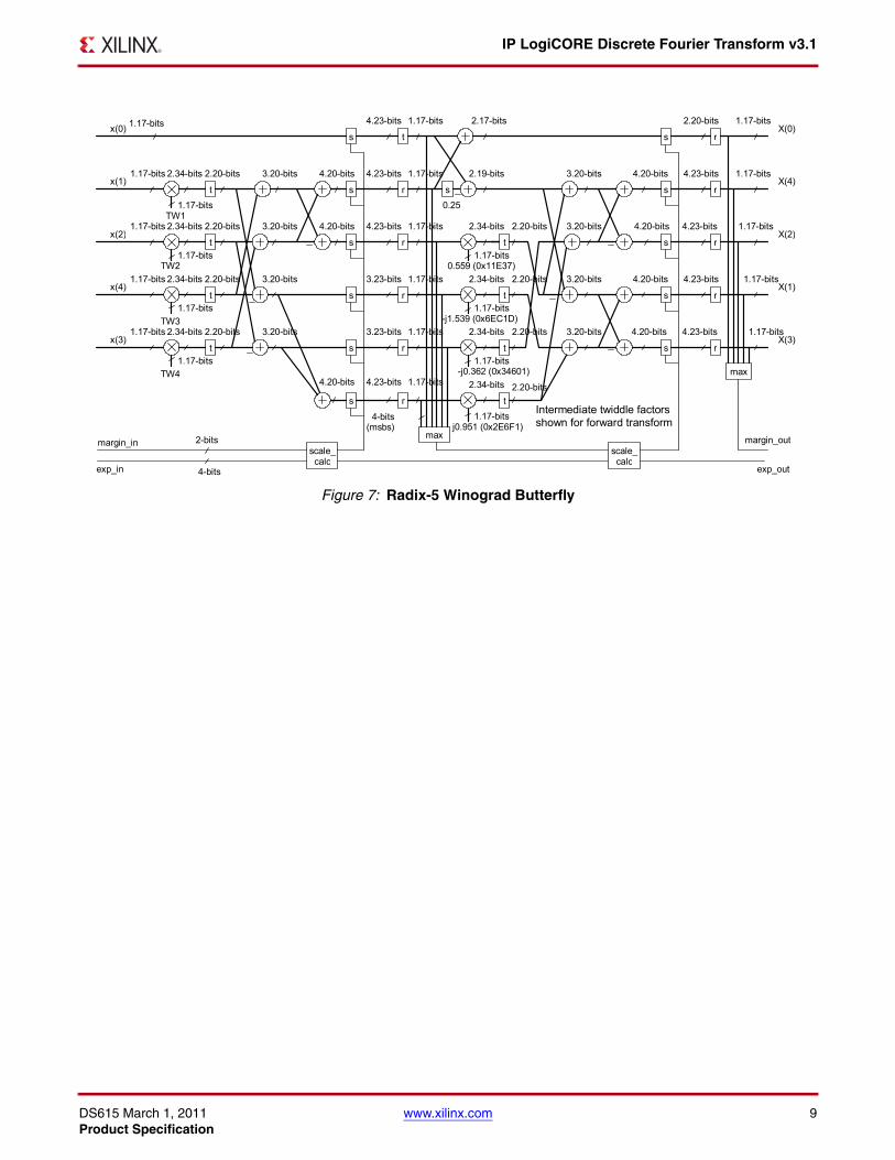
Radix-r Unit
Figure 6 and Figure 7 show the radix-3 and radix-5 butterfly operations used by the DFT. They include the twiddlefactor multiplications on the input required to cascade factors to obtain a 2M*3P*5Q point DFT. The diagrams alsoshow the internal word lengths adopted, and include the scaling and rounding blocks required to implementblock-floating-point. Their function is explained in the next section.
The radix-5 butterfly is performed using two passes of the radix-r unit. The first pass performs the twiddle-factormultiplications and first two stages of adders. At this point, scaling and rounding are applied to reduce word lengthto that of the input, so that it may be fed back for the second pass. The worst-case word growth for the first half isequivalent to that of the whole butterfly, so no further scaling is applied in the second pass. The second pass per-forms the intermediate multiplies and the final two stages of addition. Quantization reduces the word length to thatof the input, so that it may be stored in the intermediate memory, ready for the next stage.
X-Ref Target - Figure 6
Figure 6: Radix-3 Winograd Butterfly
j0.866 (0x1BB68)
TW 1 0.5
r s t
t r s
max
TW 2
2.20-bits
1.17-bits
x(0)
x(1)
x(2)
scale_calc
X(1)
X(2)
3.20-b its1.17-bits
t
t
t
4.20-bits 4.20-b its 1.17-b its
margin_in
exp_in exp_out
margin_out
X(0)r s
3.20-bits
4.20-bits
4.20-bits
1.17-bits
1.17-b its
2.34-bits
4.37-bits
t Truncation
r Round (to nearest) w ith saturation
4-bits (msbs)
2-bits
4-bits
1.17-bits
1.17-bits
1.17-bits
s Shif t right by 1-b it
3.20-bits2.34-bits 2.20-b its
4.20-bits 4.20-bits
4.20-bits
1.17-bits
4.20-b its Two’s complement fixed-point number with 20 fract ional
Key
4.23-bits
4.23-bits
4.23-bits
s
3.21-bits
s Shif t
0.5
DS615 March 1, 2011 www.xilinx.com 9Product Specification
IP LogiCORE Discrete Fourier Transform v3.1
X-Ref Target - Figure 7
Figure 7: Radix-5 Winograd Butterfly
j0.951 (0x2E6F1)
-j0.362 (0x34601)
-j1.539 (0x6EC1D)
0.559 (0x11E37)
TW1 0.25
r s t
t
t
t
r s
r s
r s
max
TW2
TW3
TW4
2.20-bits
1.17-bits
x(0)
x(1)
x(2)
x(3)
x(4)
s
s
s
s
r
r
r
r
max
scale_calc
scale_calc
s r
X(0)
X(4)
X(2)
X(3)
X(1)
3.20-bits 4.20-bits
t
t
t
3.20-bits 4.20-bits
t
margin_in
exp_in exp_out
margin_out
r s
4-bits (msbs)
4-bits
2-bits
2.34-bits
s
2.17-bits
s 1.17-bits
t
4.20-bits
4.20-bits
4.20-bits
4.23-bits
Intermediate twiddle factors shown for forward transform
4.23-bits
4.23-bits
4.23-bits
4.23-bits
1.17-bits
1.17-bits
1.17-bits
1.17-bits
2.34-bits
2.34-bits
2.34-bits
2.20-bits
2.20-bits
2.20-bits
3.20-bits
3.20-bits
3.20-bits
4.20-bits
4.20-bits
4.23-bits
3.23-bits
3.23-bits
4.23-bits
4.23-bits
2.19-bits
2.34-bits
2.34-bits
2.34-bits
2.20-bits
2.20-bits
2.20-bits
2.20-bits2.34-bits
1.17-bits
1.17-bits
1.17-bits 1.17-bits
1.17-bits
1.17-bits
1.17-bits
3.20-bits
3.20-bits
3.20-bits
2.20-bits 1.17-bits
1.17-bits
1.17-bits
1.17-bits
1.17-bits
1.17-bits
1.17-bits
1.17-bits
1.17-bits
1.17-bits
1.17-bits

DS615 March 1, 2011 www.xilinx.com 10Product Specification
IP LogiCORE Discrete Fourier Transform v3.1
Block Floating-Point Behavior
Word length growth within the transform is accommodated by block floating-point. This is achieved by scaling theoutput of the radix-r unit by a power of 2 to keep a data word length of 18-bits. To reduce implementation cost, thelevel of scaling is either 0, 1, 2 or 3-bit shift, allowing its implementation using a 4-1 multiplexer.
The level of scaling is calculated by establishing the maximum size of the layer input, and the maximum wordgrowth possible through the layer.
This growth is bits per radix-r layer. The scaling occurs when a complex input with full-scalepositive or negative real or imaginary parts, is rotated by 45 degrees. Rotations are required between layers as aresult of the factorization of the DFT algorithm. The first layer requires no twiddle-factors, and so the word growthis exactly 2 bits and the associated scaling is 1/4, which is obtained by a 2-bit right-shift. The worst-case scalingapplied for each radix is summarized in Table 3.
The maximum absolute value of the input is establish by examining the butterfly output from the previous layer.This examination is done as the outputs are calculated and written to memory, and so the final value is the maxi-mum across the whole layer. To minimize resources, the butterfly outputs are truncated to 4 bits before the absolutevalue is calculated.
The maximum absolute value is used to establish a margin, in terms of bits. This margin is the number of bits bywhich an input might grow without overflow (that is, the number of leading zeros or ones, excluding sign in thelargest term).
The required scaling is, therefore, the worst-case scaling reduced by the margin, with negative values being set tozero. The scaling applied at each layer is summed, and provided as the block floating-point exponent with the com-plex output data.
Table 3: Power-of-2 Scaling Required to Accommodate Worst-Case Growth
Radix-4 Layer Worst-Case Growth Power-2 Scaling
Radix-2 2.414 4
Radix-3 3.828 4
Radix-4 First layer 2.000 2
Radix-4 Other layer 5.243 8
Radix-5 6.657 8
Table 4: Establishing Margin from the Maximum Absolute Value
Maximum Absolute Value (x) Margin
0
1
2
3
log2 1 r 1–( ) 2+( ) 2
x 0.5≥
0.25 x 0.5<≤
0.125 x 0.25<≤
x 0.125<
DS615 March 1, 2011 www.xilinx.com 11Product Specification
IP LogiCORE Discrete Fourier Transform v3.1
ResourcesLUT counts include SRL16s or SRL32s (according to device family).The tool settings to achieve these results were as follows:map -ol highpar -ol high
Note: The tool settings can have a significant effect on area use and speed. The Xilinx Xplorer script can be used to find the optimal settings.
Note: Resource utilization and clock frequencies are provided as a guide only. They may vary with new releases of the Xilinx implementation tools. Clock frequency does not take jitter into account and should be derated by an amount appropriate to the clock source jitter specification.
The figures below were obtained using speedfile versions:
• Virtex-6: ADVANCED 1.02d 2009-10-07
• Virtex-5: PRODUCTION 1.66 2009-10-13
• Spartan-6: ADVANCED 1.02d 2009-10-07
• Spartan-3A DSP: PRODUCTION1.33 2009-10-13
The resources and maximum operating frequencies are summarized in Table 5.

DS615 March 1, 2011 www.xilinx.com 12Product Specification
IP LogiCORE Discrete Fourier Transform v3.1
References1. 3GPP TS 36.211 v8.0.0 (2007-2009) Physical channels and modulation. Evolved Universal Terrestrial Radio Access
(E-UTRA); Technical Specification Group Radio Access Network; 3rd Generation Partnership Project.
Support Xilinx provides technical support at www.xilinx.com/support for this LogiCORE product when used as describedin the product documentation. Xilinx cannot guarantee timing, functionality, or support of product if implementedin devices that are not defined in the documentation, if customized beyond that allowed in the productdocumentation, or if changes are made to any section of the design labeled DO NOT MODIFY.
Refer to the IP Release Notes Guide (XTP025) for further information on this core. On the first page there is a link to“All DSP IP.” The relevant core can then be selected from the displayed list.
Table 5: Resources and Speed of the DFT Core
Family Sync.Clear
Clock Enable
Input/Output
Data Width
Number of
Slices/LUT6-FF Pairs(1)
LUTs FFs
Block RAMs
(RAM36/18)(1)
DSP48 Fmax(MHz) Part Speed
Virtex-6 no no 8 3743 3670 3403 3/4 16 332 XC6VLX75T 1
18 3820 3733 3460 16 339
yes 8 5031 4948 4637 16 318
18 5135 5041 4694 16 318
yes 8 3829 3753 3460 16 310
18 5123 5046 4694 16 318
Virtex-5 no no 8 4366 3427 3479 3/4 16 310 XC5VLX85 1
18 5746 4687 4664 283
yes 8 4432 3447 3558 318
18 5796 4707 4743 276
yes 8 4443 3590 3536 283
18 5847 4851 4721 283
Spartan-6 no no 8 3615 3524 3395 7 156 XC6SLX75T 2
18 4793 4701 4609 165
yes 8 3667 3596 3451 156
18 4844 4726 4665 165
yes 8 3714 3629 3451 156
18 4881 4785 4665 149
Spartan-3ADSP
no no 8 2899 4409 3467 7 145 XC3SD3400A 1
18 3706 5661 4699 150
yes 8 2955 4461 3546 152
18 3763 5713 4778 148
yes 8 2939 4552 3525 117
18 3754 5804 4757 132
Notes: 1. For Spartan-6, Virtex-5, Virtex-6 FPGA family only.
DS615 March 1, 2011 www.xilinx.com 13Product Specification
IP LogiCORE Discrete Fourier Transform v3.1
For each core, there is a master Answer Record that contains the Release Notes and Known Issues list for the corebeing used. The following information is listed for each version of the core:
• New Features
• Bug Fixes
• Known Issues
Ordering InformationThis LogiCORE IP module is included at no additional cost with the Xilinx ISE Design Suite software and is provided under the terms of the Xilinx End User License Agreement. Use the CORE Generator software included with the ISE Design Suite to generate the core. For more information, please visit the core page.
Information about additional Xilinx LogiCORE modules is available at the Xilinx IP Center. For pricing and availability of other Xilinx LogiCORE modules and software, please contact your local Xilinx sales representative.
Revision HistoryThe following table shows the revision history for this document.
Notice of DisclaimerXilinx is providing this product documentation, hereinafter “Information,” to you “AS IS” with no warranty of any kind, expressor implied. Xilinx makes no representation that the Information, or any particular implementation thereof, is free from anyclaims of infringement. You are responsible for obtaining any rights you may require for any implementation based on theInformation. All specifications are subject to change without notice. XILINX EXPRESSLY DISCLAIMS ANY WARRANTYWHATSOEVER WITH RESPECT TO THE ADEQUACY OF THE INFORMATION OR ANY IMPLEMENTATION BASEDTHEREON, INCLUDING BUT NOT LIMITED TO ANY WARRANTIES OR REPRESENTATIONS THAT THISIMPLEMENTATION IS FREE FROM CLAIMS OF INFRINGEMENT AND ANY IMPLIED WARRANTIES OFMERCHANTABILITY OR FITNESS FOR A PARTICULAR PURPOSE. Except as stated herein, none of the Information may becopied, reproduced, distributed, republished, downloaded, displayed, posted, or transmitted in any form or by any meansincluding, but not limited to, electronic, mechanical, photocopying, recording, or otherwise, without the prior written consent ofXilinx.
Date Version Revision
03/24/08 1.0 Initial Xilinx release.
06/27/08 2.0 Updated for core version v3.0.
06/24/09 3.1 Clarified DIN and DOUT in Functional Overview section of data sheet. Updated Ordering Information section to remove “full license” requirement.
12/02/09 3.2 Updated licensing, support, and speed file information. Modified Figure 6.
03/01/11 3.3 Support added for Virtex-7 and Kintex-7. ISE Design Suite 13.1
Related Documents