NEXIP HIGH-END COMPUTER VISION ALGORITHMS IMAGE PROCESSING & ANALYSIS GPU-FPGA 2016 Catalog

Welcome message from author
This document is posted to help you gain knowledge. Please leave a comment to let me know what you think about it! Share it to your friends and learn new things together.
Transcript

NEXIPHIGH-END COMPUTER VISION ALGORITHMSIMAGE PROCESSING & ANALYSISGPU-FPGA2016 Catalog

/// 002 | NEXIP™ www.nexvision.fr | [email protected] | (+33) 4 91 77 62 86 | MARSEILLE - FRANCE
NEXIPHIGH-END COMPUTER VISION ALGORITHMSIMAGE PROCESSING & ANALYSIS2016 Catalog
powered by

NEXIP™ | 003 ///
SUMMARY
ABOUT NEXVISION
ABOUT THE NEXIP LIBRARY
VIDEO OUTPUT algorithms
IMAGE ANALYSIS algorithms
IMAGE PROCESSING algorithms
IMAGE CAPTURE algorithms
Optical
Pre-processing
Enhancement
DATA LINK algorithms
MISCELLANEOUS algorithms

/// 004 | NEXIP™
NEXVISION designs and manufactures advanced optronics for innovative vision systems with a rare level of expertise in the world.
We develop whole multispectral systems, from Hardware to Software, in-cluding cutting-edge image processing and analysis algorithms.
Nexvision masters the entire vision system architecture :
Image sensors integration in each spectral band (UV, visible, night, SWIR, LWIR, Thermal, Terahertz)
Thanks to our powerful electronic modular architecture, we can quickly de-sign any complex vision system, so our customers usually save 30% to 50% in development time.
HPC embedded electronic design (CPU/GPU/CUDA/FPGA…)
Image processing & analysis software
Video streaming, video over IP & high speed real time trans-mission.
ABOUT NEXVISION
We design complex optronics for several markets.
SECURITY / DEFENSE / AEROSPACE
SMART HOME /SMART CITIES
CINEMA / MEDIA
INDUSTRIAL INSPECTION

NEXIP™ | 005 ///
SECURITY / DEFENSE / AEROSPACE
SMART HOME /SMART CITIES
CINEMA / MEDIA
INDUSTRIAL INSPECTION

/// 006 | NEXIP™
NEXIP™ is our IP library running on FPGA and GPU.
Our algorithms are actually used in several optronics for differents markets (night vision system for helicopter pilot’s helmet, digital microscope, videosurveillance system in the A380...).
Our portfolio of imaging and vision solutions is constantly expanded and compatible with the latest OEM technologies(Xilinx Kintex 7 & Ultrascale FPGA, nVidia Tegra K1/X1…).
ABOUT NEXIP™

NEXIP™ | 007 ///
Our complete library at a glance :
PRE PROCESSING ENHANCEMENT
OPTICAL ENHANCEMENT& CORRECTIONS > Super resolution > Aberration corrections > Chromatic aberrations > Relative illumination > Distorsion correction > Fisheye correction
IMAGE SENSOR PREPROCESSING > CFA Bayer to RGB > Auto exposure > Multi resolution > Color matrix correction > Auto white balance > Gamma & YUV/HSI color conversion > Dead pixel correction > Non uniformity correction (FPN) > DSNU & PRNU > Anti flickering > Lab color space conversion > 2D Image scaling > 3D lookup table color correction > ACES color space management
DYNAMIC RANGE : HDR& NOISE FILTERING > High Dynamic Range > Dynamic local tone mapping > 3D noise filter > Contrasts & edges enhancement > Spatial filters
Methods > Feature extraction > Pattern matching > Texture recognition > Optical Character Recognition > Smart line detection (rail, lane, path, horizon) > Multispectral band object recognition > Content based image retrieval
OPTICAL
DECONVOLUTION > Image reconstitution > Recursive algorithms > Denoising > Myopic deconvolution > Lens defocused > Multi channels deconvolution
STABILIZATION > Close control loop > Piezo actuator > Motion compensation > Viewer pointed
VIBRATION CORRECTION ENVIRONMENT MEASUREMENT > Augmented reality > SLAM > 3D scene reconstruction > Localisation / positioning > Advanced Driver Assistance System > Ground speed estimate > Unified scene alignment > Depth map > Sensors fusion > Barcode / QR Code reading > 1D, 2D, 3D measurement
IMAGE CAPTURE
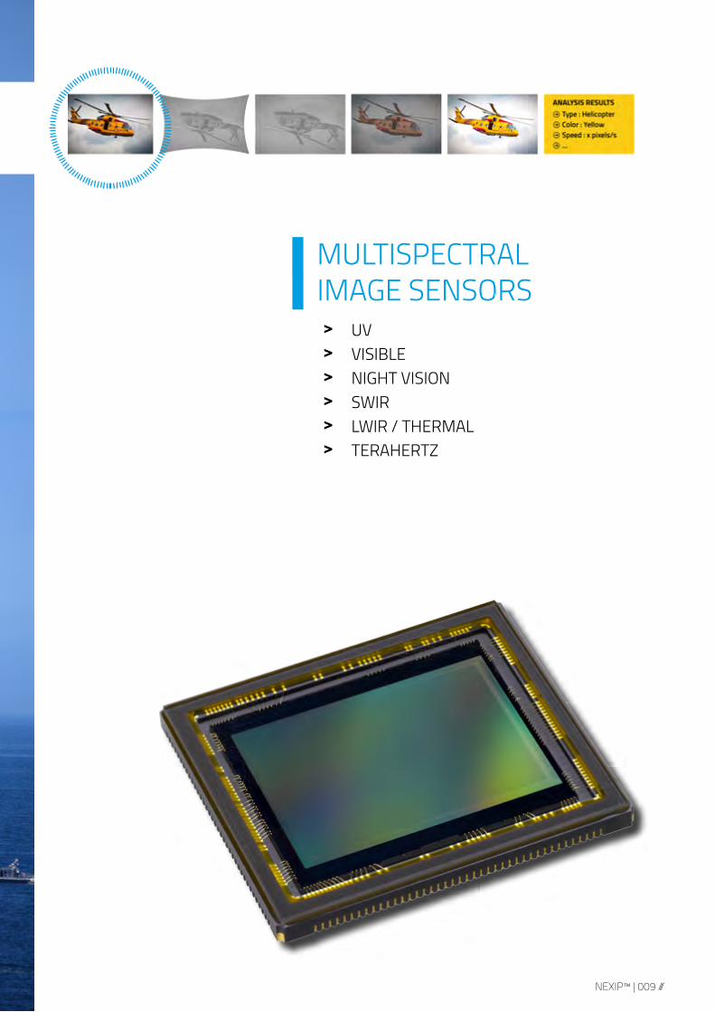
MULTISPECTRALIMAGE SENSORS > UV > Visible > Night vision > SWIR > LWIR / Thermal > TeraHertz
DISPLAY > Microoled > LCD
I/O > Composite > HDMI > SDI (3G-HD) > CoaXPress
ANALYSIS RESULTSType : HelicopterColor : YellowSpeed : x pixels/s...
ANALYSIS
MACHINE LEARNING > Shallow learning > Deep learning > Neural networks
TRACKING > Online tracking > Specialized trackers > Autonomous tracking initialization
Applications > Suspicious stationary object detection > Motion detection > Number plate recognition > Traffic accident detection > Streetcar line detection > Fire detection > Pedestrian counting > Human body detection > Gesture recognition
DETECTION / RECOGNITION
VIDEO OUTPUTDATA LINK
I/O > PCIe (FPGA Tegra DMA) > USB 2.0, 3.0 & 3.1 > NVMe / SSD > Fiber-optic interconnect
MISCELLANEOUS IP > Master AXI Lite Intf > AXI Lite Slave Intf > I2C driver
> SPI driver > Flash SPI > PWM

IMAGE CAPTURE algorithms
NEXIP™ | 009 ///
▌MULTISPECTRAL ▌ IMAGE SENSORS
> UV > VISIBLE > NIGHT VISION > SWIR > LWIR / THERMAL > TERAHERTZ

/// 010 | NEXIP™
/// APPLICATIONS/// IP FEATURES
/// BLOCK DIAGRAM
░ Visible | Python driver
• Support 0.3, 0.5 and 1.3 Megapixels sensor’s version• Up to 815 FPS• 8 Bit or 10 Bit output mode• LVDS data and control links calibration• Sensor configuration (through an SPI connection) • 3 Exposure control modes• Sensor’s temperature reading• Configurable frame size
This IP controls OnSemi Python video sensor and delivers video frames based on data received from the sensor.
XILINX ARTIX 7 SERIESGeneric Parameter Device Resources Performance
PIXEL WIDTH SENSOR VERSION Luts Flip-Flops Bram DSP48 Fmax
10 0.3 Mpx 1328 976 1 0 Serial Clock 360 MHz
Provided with IP
Documentation Design Specification
Validation Specification
Implementation Specification
Design Files VHDL
Example Design Provided
Test Bench VHDL
Simulation Model VHDL
Constraints File XDC
IP Core Specifics
Supported Device Family Xilinx 7 series
Design Flow
Design Entry Vivado @Design Suite
Simulation Isim
Synthesis Vivado Synthesis
• High frame rate video applications
NEXIP™ | 011 ///
/// APPLICATIONS/// IP FEATURES
/// ABOUT THE KAMELEON SENSOR
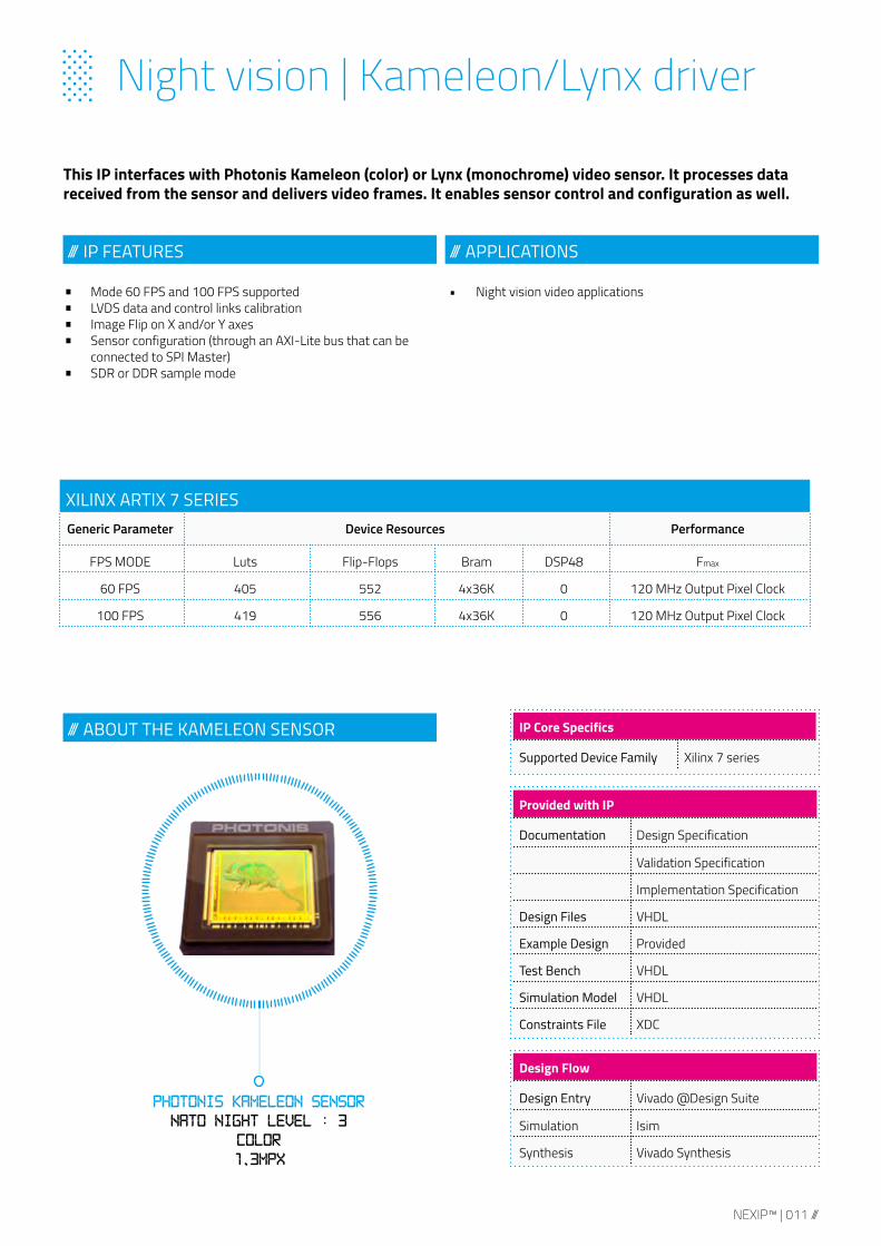
░ Night vision | Kameleon/Lynx driver
This IP interfaces with Photonis Kameleon (color) or Lynx (monochrome) video sensor. It processes data received from the sensor and delivers video frames. It enables sensor control and configuration as well.
• Mode 60 FPS and 100 FPS supported• LVDS data and control links calibration• Image Flip on X and/or Y axes• Sensor configuration (through an AXI-Lite bus that can be
connected to SPI Master) • SDR or DDR sample mode
• Night vision video applications
XILINX ARTIX 7 SERIESGeneric Parameter Device Resources Performance
FPS MODE Luts Flip-Flops Bram DSP48 Fmax
60 FPS 405 552 4x36K 0 120 MHz Output Pixel Clock
100 FPS 419 556 4x36K 0 120 MHz Output Pixel Clock
Provided with IP
Documentation Design Specification
Validation Specification
Implementation Specification
Design Files VHDL
Example Design Provided
Test Bench VHDL
Simulation Model VHDL
Constraints File XDC
IP Core Specifics
Supported Device Family Xilinx 7 series
Design Flow
Design Entry Vivado @Design Suite
Simulation Isim
Synthesis Vivado Synthesis
Photonis Kameleon sensor
NATO night level : 3
Color
1,3MpX

/// 012 | NEXIP™
/// APPLICATIONS/// IP FEATURES
/// BLOCK DIAGRAM
░ Visible | CMV driver
• Support all CMOSIS CMV devices.• Support external exposure control.• Support 10 bits per pixel mode.• Support X and/or Y axes flipping.• Support DDR sample mode.• Sensor configuration through an AXI-Lite bus which can be
connected to AXI-Lite Master.• LVDS data and control links calibration.• Configurable number of LVDS data outputs• Configurable number of pixels per clock.• Can take into account the vibrations of the system for expo-
sure management.• Provide a Frame, Line and Pixel to downstream IP.
This IP interfaces with CMOSIS CMV video sensor. It processes data received from the sensor and delivers video frames.It enables sensor control and configuration as well.
XILINX ARTIX 7 : XC7A200TFBG676Generic Parameter Device Resources Performance
PIXEL BY CLOCK
LVDS NUMBER Luts Flip-Flops Bram DSP48 Frequency
2 8 1861 2325 5x18K 0 40 MHz SDR Input Sensor200 MHz DDR Output Sensor
160 MHz SDR Output Pixel
Provided with IP
Documentation Design Specification
Validation Specification
Implementation Specification
Design Files VHDL
Example Design Not provided
Test Bench VHDL
Simulation Model Not provided
Constraints File XDC
IP Core Specifics
Supported Device Family All Xilinx 7 series & Ultrascale
Design Flow
Design Entry Vivado @Design Suite
Simulation Isim / QuestaSim
Synthesis Vivado Synthesis
• Embedded Systems• Vision enhancement, automotive or airborne • Film, photographic, graphic design, printing industries

NEXIP™ | 013 ///
/// APPLICATIONS/// IP FEATURES
░ Aptina AR1011HS driver
• Support 12 bits per pixel.• Manual exposure mode supported.• Configurable number of pixels per clock.• Sensor configuration through an I2C interface.• Sensor registers available in Read/Write mode through regis-
ter interface.• LVDS data and control links calibration: Eye detection, Word
alignment.• Support DDR sample mode for LVDS inputs.• Can control the LED light with regards to integration time.• Provide a Nexvision Video Interface based on sync signals
(Frame, Line and Pixel data) to downstream IP.
This IP interfaces with Aptina AR1011HS video sensor. It processes data received from the sensor and delivers video frames.It enables as well sensor control and configuration.
XILINX KINTEX 7 : XC7K70TFBG484-2Generic Parameter Device Resources Performance
PIXEL BY CLOCK
LVDS NU-MBER
Luts Flip-Flops Bram DSP48 IDELAY LVDS Frequency Pixel Frequency
8 24 1600 2800 49 0 24 288 MHz 144 MHz
Provided with IP
Documentation Design Specification
Design Files VHDL
Example Design Not provided
Test Bench Not provided
Simulation Model Not provided
Constraints File XDC
IP Core Specifics
Supported Device Family All Xilinx 7 series & Ultrascale
Design Flow
Design Entry Vivado @Design Suite
Simulation Not provided
Synthesis Vivado Synthesis
• Embedded Systems• Vision enhancement, automotive or airborne • Film, photographic, graphic design, printing industries

/// 014 | NEXIP™
/// APPLICATIONS/// IP FEATURES
/// BLOCK DIAGRAM
░ On Semiconductor AR1411HS driver
• Support 12 bits per pixel.• Manual and Automatic exposure modes supported.• Configurable number of pixels per clock.• Sensor configuration through an I2C interface.• Sensor registers available in Read/Write mode through AXI-
lite or register interface.• LVDS data and control links calibration: Eye detection, Word
alignment.• Support DDR sample mode for LVDS inputs.• Can take into account vibrations of the system for exposure
management.• Provide a Nexvision Video Interface based on sync signals
(Frame, Line and Pixel data) to downstream IP.
This IP interfaces with On Semiconductor AR1411HS video sensor. It processes data received from the sensor and delivers video frames.It enables as well sensor control and configuration.
XILINX ARTIX 7 : XC7A200TFBG676Generic Parameter Device Resources Performance
PIXEL BY CLOCK
LVDS NUMBER Luts Flip-Flops Bram DSP48 Frequency
6 24 29.16 MHz SDR Input Sensor29.16 MHz DDR Output Sensor
200 MHz SDR Output Pixel
Provided with IP
Documentation Design Specification
Validation Specification
Implementation Specification
Design Files VHDL
Example Design Not provided
Test Bench VHDL
Simulation Model Not provided
Constraints File XDC
IP Core Specifics
Supported Device Family All Xilinx 7 series & Ultrascale
Design Flow
Design Entry Vivado @Design Suite
Simulation Isim / QuestaSim
Synthesis Vivado Synthesis
• Embedded Systems• Vision enhancement, automotive or airborne • Film, photographic, graphic design, printing industries

NEXIP™ | 015 ///

IMAGE PROCESSING ▌ OPTICAL

NEXIP™ | 017 ///
▌OPTICAL ENHANCEMENT & CORRECTIONS
> SUPER RESOLUTION > ABERRATION CORRECTIONS > CHROMATIC ABERRATIONS > RELATIVE ILLUMINATION > DISTORSION CORRECTION > FISHEYE CORRECTION
▌DECONVOLUTION > IMAGE RECONSTITUTION > RECURSIVE ALGORITHMS > DENOISING > MYOPIC DECONVOLUTION > LENS DEFOCUSED > MULTI CHANNELS DECONVOLUTION
▌STABILIZATION > CLOSE CONTROL LOOP > PIEZO ACTUATOR > MOTION COMPENSATION > VIEWER POINTED
▌AUTOFOCUS

/// APPLICATIONS/// IP FEATURES
/// 018 | NEXIP™
/// RESOURCES & PERFORMANCE
/// BLOCK DIAGRAM
░ Pixel Sub Sampling 3This IP algorithm shifts frame of 1/3 of a pixel during a sequence of 36 frames to perform a 9-times up sampling of each pixel. The goal is to extract a quality enhanced RGB image directly from RAW data after having merged 9 images with external software.
• 4 Raw (10 bits) pixels by clock.• A piezo actuator to shift image of 1/3 of pixel horizontally or
vertically.• The colored sensor is organized with a bayer G1-R-G2-B
pattern.• No debayering algorithm needed.
• Industrial inspection/Machine Vision• Quality Assurance• Microscopy• Embedded Systems
Provided with IP
Software provided in C#
Documentation Design Specification
Design Files VHDL
Example Design Not provided
Test Bench VHDL
Simulation Model Not provided
Constraints File UCF
IP Core Specifics
Supported Device Family Xilinx 7 series
Design Flow
Design Entry ISE 14.6
Simulation Isim
Synthesis ISE Synthesis
Device XILINX KINTEX 7 (XC7-K325T-1FFG676)
Device Resources Performance
Luts Flip-Flops Bram DSP48 Fmax
1143 737 1 0 200 MHz

NEXIP™ | 019 ///
/// APPLICATIONS/// IP FEATURES
/// RESOURCES & PERFORMANCE/// BLOCK DIAGRAM
░ Color co-site Sub SamplingThe algorithm captures 4 frames which are shifted by 1 pixel thanks to an actuator. The objective is to extract RGB directly from RAW data instead of using a debayer.
• 4 Raw (10 bits) pixels by clock.• A piezo actuator to shift image of one pixel horizontally or
vertically.• The colored sensor is organized with a bayer G1-R-G2-B
pattern.• No debayering algorithm needed.
• Industrial inspection/Machine Vision• Quality Assurance• Microscopy• Embedded Systems
Provided with IP
Documentation Design Specification
Design Files VHDL
Example Design Not provided
Test Bench VHDL
Simulation Model Not provided
IP Core Specifics
Supported Device Family Xilinx 7 series
Design Flow
Design Entry ISE 14.6
Simulation Isim
Synthesis ISE Synthesis
Device XILINX KINTEX 7 (XC7-K325T-1FFG676)
Device Resources Performance
Luts Flip-Flops Bram DSP48 Fmax
439 661 1 0 200 MHz
/// RESOURCES & PERFORMANCE
/// 020 | NEXIP™
/// APPLICATIONS/// IP FEATURES
/// RESOURCES & PERFORMANCE
/// BLOCK DIAGRAM
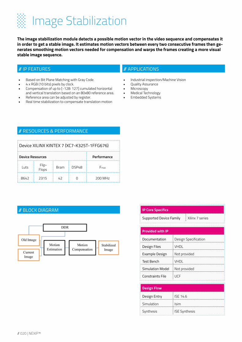
░ Image StabilizationThe image stabilization module detects a possible motion vector in the video sequence and compensates it in order to get a stable image. It estimates motion vectors between every two consecutive frames then ge-nerates smoothing motion vectors needed for compensation and warps the frames creating a more visual stable image sequence.
• Based on Bit Plane Matching with Gray Code. • 4 x RGB (10 bits) pixels by clock.• Compensation of up to [-128: 127] cumulated horizontal
and vertical translation based on an 80x80 reference area.• Reference area can be adjusted by register.• Real time stabilization to compensate translation motion
• Industrial inspection/Machine Vision• Quality Assurance• Microscopy• Medical Technology• Embedded Systems
Provided with IP
Documentation Design Specification
Design Files VHDL
Example Design Not provided
Test Bench VHDL
Simulation Model Not provided
Constraints File UCF
IP Core Specifics
Supported Device Family Xilinx 7 series
Design Flow
Design Entry ISE 14.6
Simulation Isim
Synthesis ISE Synthesis
Device XILINX KINTEX 7 (XC7-K325T-1FFG676)
Device Resources Performance
Luts Flip-Flops Bram DSP48 Fmax
8642 2315 42 0 200 MHz

NEXIP™ | 021 ///
/// APPLICATIONS/// IP FEATURES
/// RESOURCES & PERFORMANCE
/// BLOCK DIAGRAM
░ Focus Map
• 4 x RGB (10 bits) pixels by clock.• Based on the square of a gradient compared to a threshold,
to calculate the difference between a pixel and its neighbors.
• Industrial inspection/Machine Vision• Quality Assurance• Microscopy• Embedded Systems
Focus map IP divides an image in a given number of areas. The module treats the current image finding the level of information for each area and for each vertical position of the optical engine.With this module, user knows the best vertical position for each area.
Provided with IP
Documentation Design Specification
Design Files VHDL
Example Design Not provided
Test Bench VHDL
Simulation Model Not provided
Constraints File UCF
IP Core Specifics
Supported Device Family Xilinx 7 series
Design Flow
Design Entry ISE 14.6
Simulation Isim
Synthesis ISE Synthesis
Device XILINX KINTEX 7 (XC7-K325T-1FFG676)
Device Resources Performance
Luts Flip-Flops Bram DSP48 Fmax
3364 1585 5 32 200 MHz

/// 022 | NEXIP™
/// APPLICATIONS/// IP FEATURES
/// RESOURCES & PERFORMANCE
/// BLOCK DIAGRAM
░ Focus ScoreThis IP calculates the focus value of an incoming frame. It can be used in conjunction of an autofocus algorithm to change the lens position in order to deliver the sharpest image possible from a system.
• 4 x RGB (30 bits) pixels by clock.• Based on the square of a gradient compared to a threshold,
to calculate the difference between a pixel and its neighbors.
• Industrial inspection/Machine Vision• Quality Assurance• Microscopy• Embedded Systems
Provided with IP
Documentation Design Specification
Design Files VHDL
Example Design Not provided
Test Bench VHDL
Simulation Model Not provided
Constraints File UCF
IP Core Specifics
Supported Device Family Xilinx 7 series
Design Flow
Design Entry ISE 14.6
Simulation Isim
Synthesis ISE Synthesis
Device XILINX KINTEX 7 (XC7-K325T-1FFG676)
Device Resources Performance
Luts Flip-Flops Bram DSP48 Fmax
3364 1585 5 32 200 MHz

NEXIP™ | 023 ///

IMAGE PROCESSING ▌ PRE PROCESSING

NEXIP™ | 025 ///
▌ IMAGE SENSOR PRE PROCESSING
> CFA BAYER TO RGB > AUTO EXPOSURE > MULTI RESOLUTION > COLOR MATRIC CORRECTION > AUTO WHITE BALANCE > GAMMA & YUV/HSI COLOR CONVERSION > DEAD PIXEL CORRECTION > IR SENSORS NON UNIFORMITY CORRECTION > DSNU 1& PRNU > ANTI FLICKERING > LAB COLOR SPACE CONVERSION > 2D IMAGE SCALING > 3D LOOKUP TABLE COLOR CORRECTION > ACES COLOR SPACE MANAGEMENT

/// 026 | NEXIP™
/// APPLICATIONS/// IP FEATURES
/// RESOURCES & PERFORMANCE
/// BLOCK DIAGRAM
░ CFA Bayer to RGBDemosaicing IP delivers a generic algorithm of CFA Bayer pattern to RGB. Its goal is to be used with all Image sensors implementing a basic Bayer pattern. It is based on a linear Interpolation method using 5x5 filters.
• Multi-pixels by clock • Power Management: Sleep Mode• Generic Interface• Size of a pixel (PIX_SIZE): 8 to 12 bit• Nb Pixel by clock (PIX_BY_CLK): 1 to 16• Size of the Image PIX_ROW x PIX_COLUMN ( nb of ROW and
nb of column) • Real-Time adaptation of the CFA (Color Frame management)
All vision systems with image sensors (Bayer pattern)
Provided with IP
Documentation Design Specification
Validation Specification
Implementation Specification
Design Files VHDL
Example Design VHDL
Test Bench VHDL
Reference Model Matlab
Constraints File XDC
IP Core Specifics
Supported Device Family All Xilinx 7 series
Design Flow
Design Entry Vivado @Design Suite
Simulation Isim, QuestaSim, Matlab
Synthesis Vivado Synthesis
Device XILINX ARTIX 7 (XC7A200TFBG484-3)
Generic Parameter Device Resources Performance
Number pixel by clock
Pix column
Size of a pixel Luts Flip-Flops Bram DSP48 Fmax
1 1920 12 639 619 4 0 200 MHz
5 1920 12 2852 2363 4 0 200 MHz
10 1920 12 5652 4643 8 0 200 MHz
16 1920 12 9570 7530 12 0 200 MHz

NEXIP™ | 027 ///
/// RESOURCES & PERFORMANCE
/// BLOCK DIAGRAM
░ Two by two decimation ░ CFA Bayer to RGB
Demosaicing IP delivers a generic algorithm of CFA Bayer pattern to RGB. Its goal is to be used with all Image sensors implementing a basic Bayer pattern. It is based on two by two decimation algorithm.
• Multi-pixels by clock • Power Management: Sleep Mode• Generic Interface• Size of a pixel (PIX_SIZE): 8 to 12 bit• Nb Pixel by clock (PIX_BY_CLK): 1 to 16• Image width• Real-Time adaptation of the CFA (Color Filter Array)
All vision systems with image sensors (Bayer pattern)
Provided with IP
Documentation Design Specification
Validation Specification
Implementation Specification
Design Files VHDL
Example Design VHDL
Test Bench VHDL
Reference Model Matlab
Constraints File XDC
IP Core Specifics
Supported Device Family All Xilinx 7 series
Design Flow
Design Entry Vivado @Design Suite
Simulation Isim, QuestaSim, Matlab
Synthesis Vivado Synthesis
Device XILINX ARTIX 7 (XC7A200TFBG484-3)
Generic Parameter Device Resources Performance
Number pixel by clock
Pix column
Size of a pixel Luts Flip-Flops Bram DSP48 Fmax
8 3980 129 254 2 0 144 MHz
/// APPLICATIONS/// IP FEATURES

/// 028 | NEXIP™
/// RESOURCES & PERFORMANCE
/// BLOCK DIAGRAM
░ Nearest Neighbour ░ CFA Kameleon to RGB
Demosaicing IP delivers an algorithm of CFA Kameleon from Photonis night sensor to RGBW. It is based on nearest neighbour algorithm.
• Multi-pixels by clock • Support 10 bits per pixel• Power Management: Sleep Mode• Generic Interface• Nb Pixel by clock (PIX_BY_CLK): 1 to 16• Image width • Real-Time adaptation of the CFA (Color Filter Array) of Photo-
nis night sensor: Kameleon
All vision systems using a Kameleon CFA
Provided with IP
Documentation Design Specification
Design Files VHDL
Example Design Not provided
Test Bench Not provided
Reference Model Not provided
Constraints File XDC
IP Core Specifics
Supported Device Family All Xilinx 7 & Ultras-cale series
Design Flow
Design Entry Vivado @Design Suite
Simulation
Synthesis Vivado Synthesis
Device XILINX ARTIX 7 (XC7A200TFBG484-3)
Generic Parameter Device Resources Performance
Number pixel by clock Image width Luts Flip-Flops Bram DSP48 Fmax
1 1304 57 121 4 0 120 MHz
/// APPLICATIONS/// IP FEATURES

NEXIP™ | 029 ///
/// APPLICATIONS/// IP FEATURES
/// RESOURCES & PERFORMANCE
/// BLOCK DIAGRAM
░ Auto ExposureAuto Exposure IP is a fast adaptive IP that answers need of controlling exposition of a sensor in an unstable illumination conditions scene. It calculates luminance average of a picture and adjusts sensor’s exposure time to match desired luminance target. As this IP is not sensor dependant, it can be used indifferently with night or day sensor.
• Multi-pixels by clock • Power Management: Sleep Mode• Generic Interface o Size of a pixel (PIX_SIZE): 8 to 12 bit o Nb Pixel by clock (PIX_BY_CLK): 1 to 16 o Size of a picture (PIX_ROW * PIX_COLUMN) : 1 to 20 Mpx o Frequency of the update of exposure time• 2 modes Automatic and Manual• Real-Time adaptation of target of luminance desired• Real-Time adaptation of the Max and Min of exposure time• Real-Time adaptation of the value of the correction time to
added to exposure time
• Industrial inspection/Machine Vision• Quality Assurance• Microscopy• Medical Technology• Embedded Systems• Homeland Security and border surveillance• Vison enhancement (automotive or airbone)
Provided with IP
Documentation Design Specification
Validation Specification
Implementation Specification
Design Files VHDL
Example Design Not provided
Test Bench VHDL
Simulation Model VHDL
Constraints File XDC
IP Core Specifics
Supported Device Family Xilinx 7 series& Ultrascale
Design Flow
Design Entry Vivado @Design Suite
Simulation Isim, ModelSim
Synthesis Vivado Synthesis
Device XILINX KINTEX 7 (XC7K70T-2FBG484)
Generic Parameter Device Resources Performance
Number pixel by clock
Size of a pixel
Pix column
Pix row Luts Flip-Flops Bram DSP48 Fmax
1 12 5000 4000 394 273 0 0 200 MHz
16 12 5000 4000 804 533 0 0 200 MHz

/// 030 | NEXIP™
/// APPLICATIONS/// IP FEATURES
/// RESOURCES & PERFORMANCE
/// BLOCK DIAGRAM
░ RGB to YCbCrThis IP shifts incoming frames from RGB color space to YCbCr color space.
• Power Management : Sleep Mode• Generic Interface o Size of color component: 8 to 12 bit o Number of pixel by clock: 1 to 16
Provided with IP
Documentation Design Specification
Design Files VHDL
Example Design Not provided
Test Bench Not provided
Simulation Model Not provided
Constraints File Not provided
IP Core Specifics
Supported Device Family All Xilinx 6, 7 & Ultrascale series
Design Flow
Design Entry ISE / Vivado
Simulation
Synthesis ISE & Vivado Synthesis
Device XILINX KINTEX 7 (XC7K70T-2FBG484)
Generic Parameter Device Resources Performance
Number pixel by clock Size of a pixel Luts Flip-Flops Bram DSP48 Fmax
8 3x12 bits 510 758 x 36 200 MHz
All vision systems

NEXIP™ | 031 ///
/// APPLICATIONS/// IP FEATURES
/// RESOURCES & PERFORMANCE
/// BLOCK DIAGRAM
░ RGB to YUV444
This IP shifts incoming frames from RGB color space to YUV444 color space.
• Power Management : Sleep Mode• Generic Interface o Size of color component: 8 to 12 bit o Number of pixel by clock: 1 to 16
Provided with IP
Documentation Design Specification
Design Files VHDL
Example Design Not provided
Test Bench Not provided
Simulation Model Not provided
Constraints File Not provided
IP Core Specifics
Supported Device Family All Xilinx 6, 7 & Ultrascale series
Design Flow
Design Entry ISE / Vivado
Simulation
Synthesis ISE & Vivado Synthesis
Device XILINX KINTEX 7 (XC7K70T-2FBG484)
Generic Parameter Device Resources Performance
Number pixel by clock Size of a pixel Luts Flip-Flops Bram DSP48 Fmax
8 3x12 bits 510 758 x 36 200 MHz
All vision systems
/// 032 | NEXIP™
/// APPLICATIONS/// IP FEATURES
/// RESOURCES & PERFORMANCE
/// BLOCK DIAGRAM
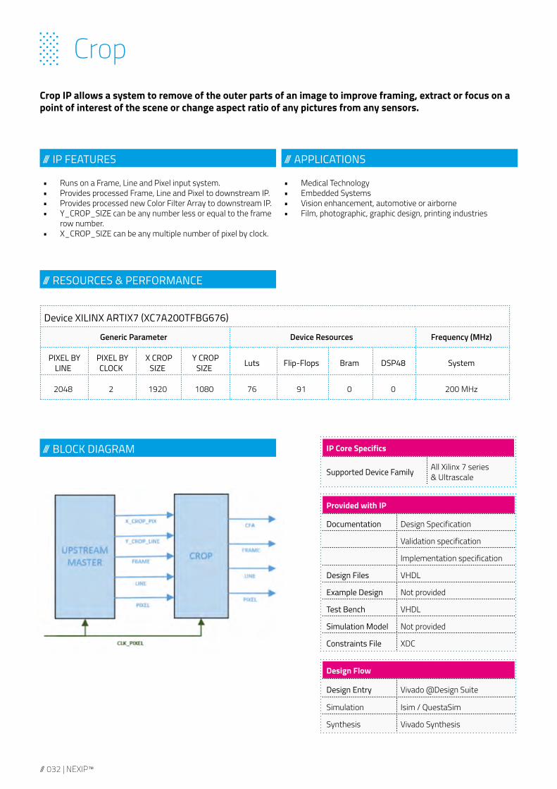
░ CropCrop IP allows a system to remove of the outer parts of an image to improve framing, extract or focus on a point of interest of the scene or change aspect ratio of any pictures from any sensors.
• Runs on a Frame, Line and Pixel input system.• Provides processed Frame, Line and Pixel to downstream IP.• Provides processed new Color Filter Array to downstream IP.• Y_CROP_SIZE can be any number less or equal to the frame
row number.• X_CROP_SIZE can be any multiple number of pixel by clock.
Provided with IP
Documentation Design Specification
Validation specification
Implementation specification
Design Files VHDL
Example Design Not provided
Test Bench VHDL
Simulation Model Not provided
Constraints File XDC
IP Core Specifics
Supported Device Family All Xilinx 7 series & Ultrascale
Design Flow
Design Entry Vivado @Design Suite
Simulation Isim / QuestaSim
Synthesis Vivado Synthesis
Device XILINX ARTIX7 (XC7A200TFBG676)
Generic Parameter Device Resources Frequency (MHz)
PIXEL BY LINE
PIXEL BY CLOCK
X CROP SIZE
Y CROP SIZE Luts Flip-Flops Bram DSP48 System
2048 2 1920 1080 76 91 0 0 200 MHz
• Medical Technology• Embedded Systems• Vision enhancement, automotive or airborne• Film, photographic, graphic design, printing industries

NEXIP™ | 033 ///
/// APPLICATIONS/// IP FEATURES
/// RESOURCES & PERFORMANCE
/// BLOCK DIAGRAM
░ Dead pixel correctionDead pixels are a common issue in vision systems and appear randomly on sensor images. This phenome-non is seen on any sensors even brand new ones. In order to solve this problem, Nexvision has designed the Dead pixel correction IP able to replace every single dead pixel by its closest neighbor.
• Up to 200 MHz system clock• Multi-pixels by clock • Low power management with global clock enable control.• Two dead pixel detection sources: o External detection along with video bus o Detection generation from a dead pixel table, available only for 1 pix/clk• Works with Monochrome or Bayer pattern pixel organization
Device XILINX ARTIX7 (XC7A200TFBG484-3)
Generic Parameter Device Resources
PIXEL SIZE PIXEL BY CLOCK DETECTION SENSOR Nb DEAD PIXEL Luts Slices Bram DSP48
8 1 Internal 20 Mpx 2048 179 258 1.5 0
8 1 External 20 Mpx 2048 23 54 0 0
8 16 External 20 Mpx 2048 326 556 0 0
All vision systems
Provided with IP
Documentation Design Specification
Validation specification
Implementation specification
Design Files VHDL
Example Design Not provided
Test Bench VHDL
Simulation Model Not provided
Constraints File XDC
IP Core Specifics
Supported Device Family All Xilinx 7 series & Ultrascale
Design Flow
Design Entry Vivado 2015.4
Simulation Isim or ModelSim
Synthesis Vivado Synthesis

/// 034 | NEXIP™
/// APPLICATIONS/// IP FEATURES
/// BLOCK DIAGRAM
/// RESOURCES & PERFORMANCE
░ Light Ring best ShotThe goal of this IP is to capture a series of 8 frames with different LED illumination configurations defined by registers. It enables to see an object with different light expositions while waiting for a proper exposure of each frame.
• 4 x (RGB 10 bits) pixels by clock.• Controls 8 LEDs around the sensor.
• Industrial inspection/Machine Vision• Quality Assurance• Microscopy• Embedded Systems
Provided with IP
Documentation Design Specification
Design Files VHDL
Example Design Not provided
Test Bench VHDL
Simulation Model Not provided
Constraints File UCF
IP Core Specifics
Supported Device Family Xilinx 7 series
Design Flow
Design Entry ISE 14.6
Simulation Isim
Synthesis ISE Synthesis
Device XILINX KINTEX 7 (XC7-K325T-1FFG676)
Device Resources Performance
Luts Flip-Flops Bram DSP48 Fmax
420 271 1 0 200 MHz

NEXIP™ | 035 ///
/// APPLICATIONS/// IP FEATURES
/// RESOURCES & PERFORMANCE
/// BLOCK DIAGRAM
░ Color matrix correctionIn camera, incoming light is split by filters into the three RGB primary colors. As filters haven’t the same response curve, RGB image from sensor has unadjusted colors. This IP corrects RGB colors delivered by the sensor.
• RGB image• Real time matrix update• Matrix 3x3 and offset• Generic Interface• Size of a pixel: 8 to 12 bitsv• Number of pixel by clock: 1 to 16
Provided with IP
Documentation Design Specification
Design Files VHDL
Example Design Not provided
Test Bench Not provided
Simulation Model Not provided
Constraints File Not provided
IP Core Specifics
Supported Device Family All Xilinx 6, 7 & Ultrascale series
Design Flow
Design Entry Vivado @Design Suite
Simulation
Synthesis ISE & Vivado Synthesis
Device XILINX KINTEX 7 (XC7K70T-2FBG484)
Generic Parameter Device Resources Performance
Number pixel by clock Size of a pixel Luts Flip-Flops Bram DSP48 Fmax
8 3x12 bits 510 758 x 36 200 MHz

/// 036 | NEXIP™
/// APPLICATIONS/// IP FEATURES
/// RESOURCES & PERFORMANCE
/// BLOCK DIAGRAM
░ Demosaicing-Linear interpolationThe NexVision IP Demosaicing is a generic algorithm of CFA Bayer pattern to RGB. The aim of this IP is to be used with all Image sensors (with basic Bayer pattern). It is based on a linear Interpolation method using 5x5 filters.
• Multi-pixels by clock • Power Management: Sleep Mode• Generic Interface o Size of a pixel (PIX_SIZE): 8 to 12 bit o Nb Pixel by clock (PIX_BY_CLK): 1 to 16 o Size of the Image PIX_ROW x PIX_COLUMN ( nb of ROW and nb of column) • Real-Time adaptation of the CFA (Color Frame management)
Provided with IP
Documentation Design Specification
Validation Specification
Implementation Specification
Design Files VHDL
Example Design VHDL
Test Bench VHDL
Reference Model Matlab
Constraints File XDC
IP Core Specifics
Supported Device Family Xilinx 7 series
Design Flow
Design Entry Vivado @Design Suite
Simulation Isim, QuestaSim, Matlab
Synthesis Vivado Synthesis
Device ARTIX 7 XC7A200TFBG484-3
Generic Parameter Device Resources Performance
Number pixel by clock
Size of a pixel
Pix column Luts Flip-Flops Bram DSP48 Fmax
1 12 1920 639 619 4 0 200 MHz
5 12 1920 2852 2363 4 0 200 MHz
10 12 1920 5652 4643 8 0 200 MHz
16 12 1900 9570 7530 12 0 200 MHz

NEXIP™ | 037 ///
/// APPLICATIONS/// IP FEATURES
/// RESOURCES & PERFORMANCE
/// BLOCK DIAGRAM
░ FPN : Fixed Pattern Noise ░ 2 Points correction | DSNU & PRNU
Nexvision FPN 2 points correction IP is made to compensate fixed pattern noise issues from an image driver. Corrective algorithm used is based on a coefficient table dependant on sensor’s physical characteris-tics. Various input parameters award great flexibility of use for all type of image sensors.
• Global Sleeping Mode (option)• Power management: automatic idle during frame blanking• Generic Interface o Size of a pixel (PIX_SIZE) o Nb pixel by clock (PIX_BY_CLK): o Size for coefficient values o Memory management for reading coefficient values• Algorithm built on gain and offset approximation• Correction results with fractional approximation• Real-Time update of coefficient table• Independent memory management for reading input calibra-
tion values
• Industrial inspection/Machine Vision• Quality Assurance• Microscopy• Medical Technology• Embedded Systems• Homeland Security and border surveillance• Vison enhancement (automotive or airbone)
(*) only if optional sleeping mode is activated
Provided with IP
Documentation Design Specification
Validation Specification
Implementation Specification
Design Files VHDL
Example Design Not Provided
Test Bench VHDL
Simulation Model Matlab
Constraints File XDC
Design Flow
Design Entry Vivado @Design Suite
Simulation Isim
Synthesis Vivado Synthesis
IP Core Specifics
Supported Device Family Xilinx 7 series& Ultrascale
Device ARTIX 7 XC7A200TFBG484-3
Generic Parameter Device Resources
Number pixel by clock
Size of a pixel
FPN_A_Size /FPN_B_Size Luts Slice
registers Bram DSP48 BUFHCE(*)
4 8 8 462 750 - - 1
8 10 8 232 950 - 8 1
16 12 8 529 1814 - 16 1

IMAGE PROCESSING ▌ ENHANCEMENT

NEXIP™ | 039 ///
▌ ENHANCEMENT ▌DYNAMIC RANGE : HDR & NOISE FILTERING
> HDR > DYNAMIC LOCAL TONE MAPPING > 3D NOISE FILTER > CONTRASTS & EDGES ENHANCEMENT > SPATIAL FILTERS
▌VIBRATION CORRECTION

/// 040 | NEXIP™
/// RESOURCES & PERFORMANCE
/// APPLICATIONS/// IP FEATURES
/// BLOCK DIAGRAM
░ High dynamic range and global tone ░ mapping (16 bits resolution based)
High-dynamic-range imaging is a set of techniques used to reproduce a greater dynamic range of lumino-sity in a picture. HDR images represent more accurately the range of intensity levels found in real scenes.Non-HDR cameras take pictures with a limited exposure range, resulting in the loss of detail in bright or dark areas. HDR compensates for this loss of detail by capturing multiple pictures at different exposure levels and combining them in order to deliver a broader tonal range picture. This IP, therefore, does mer-ging of several exposed pictures and applies a global tone mapping algorithm on the resulting picture prior to deliver it.
• 4 RGB888 pixels by clock• Merge 3 images to 1• “stop” modes: 1, 2 and 3 stops• Real time merging (16bits resolution based)• Real time global tone mapping
Provided with IP
Documentation Design Specification
Design Files VHDL
Example Design Not provided
Test Bench Not provided
Simulation Model Not provided
Constraints File Not provided
IP Core Specifics
Supported Device Family Xilinx 7 series
Design Flow
Design Entry ISE 14.6
Simulation
Synthesis ISE Synthesis
Device XILINX KINTEX 7 (XC7-K325T-1FFG676)
Device Resources Performance
Luts Flip-Flops Bram DSP48
DDR Band-width
Fmax
6215 1778 7 13 40 Gbps 200 MHz
NEXIP™ | 041 ///
/// APPLICATIONS/// IP FEATURES
/// RESOURCES & PERFORMANCE
/// BLOCK DIAGRAM
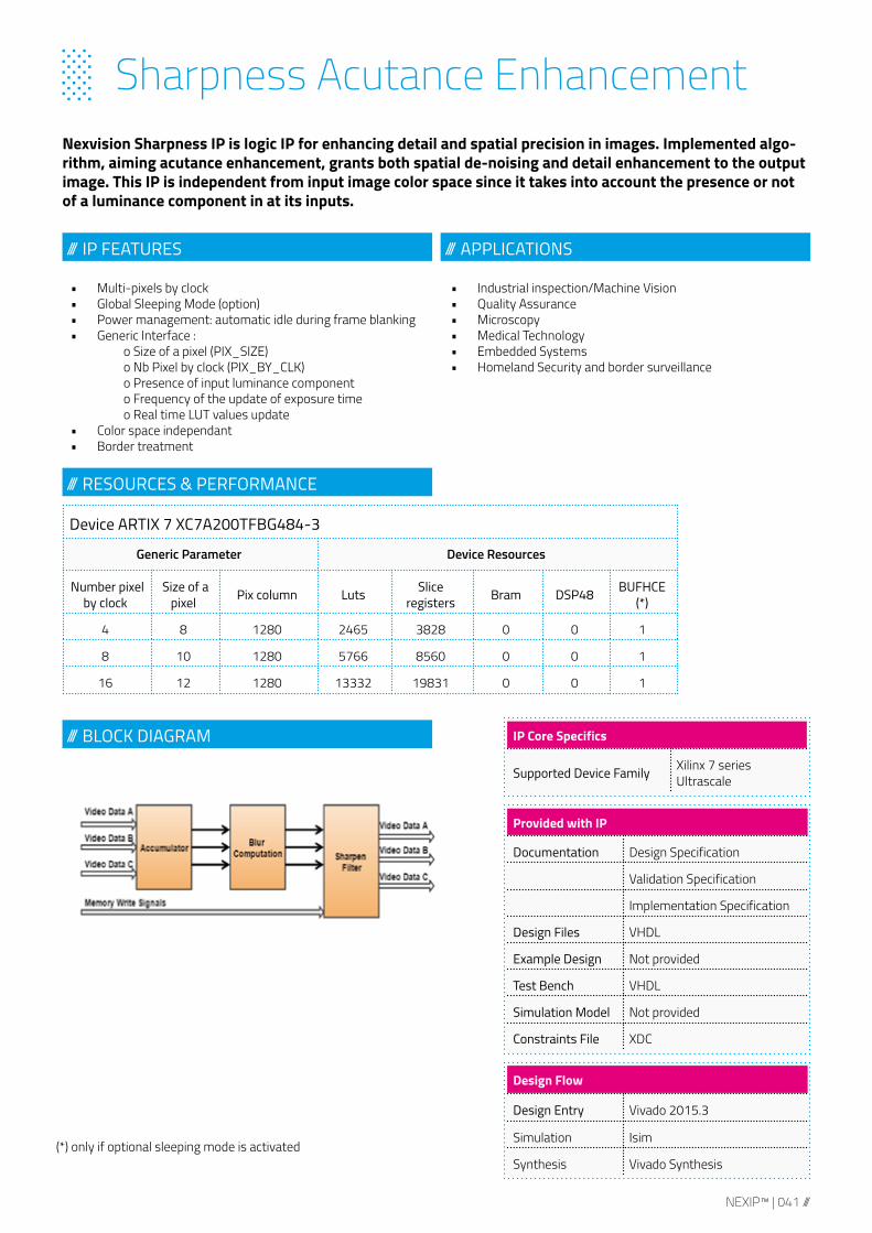
░ Sharpness Acutance EnhancementNexvision Sharpness IP is logic IP for enhancing detail and spatial precision in images. Implemented algo-rithm, aiming acutance enhancement, grants both spatial de-noising and detail enhancement to the output image. This IP is independent from input image color space since it takes into account the presence or not of a luminance component in at its inputs.
• Multi-pixels by clock • Global Sleeping Mode (option)• Power management: automatic idle during frame blanking• Generic Interface : o Size of a pixel (PIX_SIZE) o Nb Pixel by clock (PIX_BY_CLK) o Presence of input luminance component o Frequency of the update of exposure time o Real time LUT values update• Color space independant• Border treatment
• Industrial inspection/Machine Vision• Quality Assurance• Microscopy• Medical Technology• Embedded Systems• Homeland Security and border surveillance
(*) only if optional sleeping mode is activated
Provided with IP
Documentation Design Specification
Validation Specification
Implementation Specification
Design Files VHDL
Example Design Not provided
Test Bench VHDL
Simulation Model Not provided
Constraints File XDC
IP Core Specifics
Supported Device Family Xilinx 7 seriesUltrascale
Design Flow
Design Entry Vivado 2015.3
Simulation Isim
Synthesis Vivado Synthesis
Device ARTIX 7 XC7A200TFBG484-3
Generic Parameter Device Resources
Number pixel by clock
Size of a pixel Pix column Luts Slice
registers Bram DSP48 BUFHCE(*)
4 8 1280 2465 3828 0 0 1
8 10 1280 5766 8560 0 0 1
16 12 1280 13332 19831 0 0 1

IMAGE ANALYSIS

NEXIP™ | 043 ///
▌DETECTION, RECOGNITION ▌& TRACKING
> FEATURE POINT EXTRACTION > PATTERN MATCHING > LINES DETECTION > SUSPICIOUS STATIONARY OBJECT DETECTION > PEDESTRIAN COUNTING > GESTURE RECOGNITION > QUERY-BY-CONTENT > MULTISPECTRAL BAND OBJECT RECOGNITION > HUMAN BODY DETECTION > TEXTURE RECOGNITION > TRAFFIC ACCIDENT DETECTION > FIRE DETECTION > COLOR ANALYSIS

/// IP FEATURES
/// PIPELINE
░ BICTS : Binary Image Classification Training System
Nexvision Binary Image Classification Training System (BICTS) gives to Computer Vision Developers the ability to setup binary classification trainings very easily, without having to deal with cumbersome intermediary tasks.Download your dataset, let yourself be guided by BICTS while setting up the training, and enjoy your freshly new built classification model.
• SVM Training with HOG features.• Negatives auto-cropping.• Data preprocessing.• Boosted training with Multi-Process Mode.• Guided configuration setup.• Dynamic out-of-memory prevention system.• Post-Recommandations on Model usage.• Very well-tested on pedestrian INRIA Dataset.
/// 044 | NEXIP™

NEXIP™ | 045 ///
/// APPLICATIONS/// IP FEATURES
/// RESOURCES & PERFORMANCE
• Real time detection on embedded devices.• Compatible with all NVIDIA CUDA-enabled devices including
with Tegra K1/X1 processors.• Ability to train you own detector from a dataset.• Provide APIs allowing the user to have control over ro-
bustness and/or speed.
• Subway Surveillance• Driving Assistance• Embedded Systems
IP Core Specifics
Supported Device Family NVIDIA CUDA-enabled Devices
Documentation Technical report version 0.8
Host language C/C++
Device language CUDA
Device : Embedded NVIDIA Tegra K1 (A15 + GK20A)
Device Resources Performance
Architecture Compute Capability CUDA Cores GPU Clock L2 Cache Memory
Bandwidth Fmax
Kepler 3.2 192 850 MHz 128 KB 14 Gb/s 20 Hz on 640x480 Images
Device : NVIDIA Quadro K620
Device Resources Performance
Architecture Compute Capability CUDA Cores GPU Clock L2 Cache Memory
Bandwidth Fmax
Maxwell 5.0 384 1120 MHz 2048 KB 28 Gb/s 100 Hz on 640x480 Images
░ Pedestrian DetectionThe pedestrian Detection module detects walking pedestrians within various and changing environments in real time. Powered with Machine Learning and Computer Vision Algorithms, it shall give you solid & relevant detections.

/// IP FEATURES
/// PERFORMANCE (IN FRAME / SECONDS)
░ Line Tracking ░ Versatile Line Tracker for Transportation Vehicles
• Real-time Processing on embedded platforms.• Versatility: Application to automotive, tramways, trains and
so on … • Flexibility: Provides APIs allowing user to have control over
robustness and/or speed.• Lane Departure Warnings.• Leverages CUDA / GPGPU Technology.
Designed specifically for transportation vehicles, this module dynamically adapts itself to the surrounding environment. Whether the vehicle moves across rails or highways, the driver shall be shown relevant & ro-bust tracks. In addition to that, it provides lane departure warnings.
/// SCREENSHOTS
TEGRA K1 / X1 (Embedded) WORKSTATION (Intel i7, Quadro K620)
Up to 30 Up to 150
/// 046 | NEXIP™
NEXIP™ | 047 ///
/// IP FEATURES
• Real time Processing on Embedded platforms.• Simultaneous Rail detection and Pedestrian detection.• Support for Multi-GPU hardware.• Support for CPU Multithreading.• Leverages CUDA / GPGPU Technology.• Flexibility: Provides APIs allowing user to have control over
robustness and/or speed.
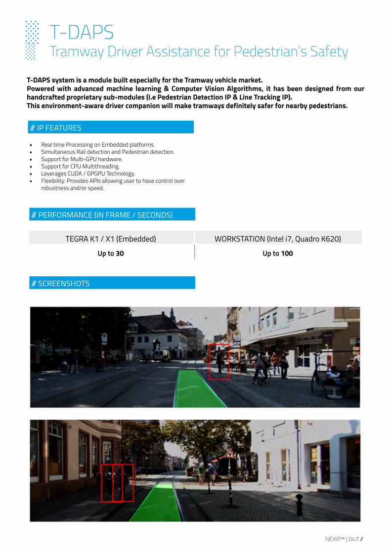
░ T-DAPS ░ Tramway Driver Assistance for Pedestrian’s Safety
T-DAPS system is a module built especially for the Tramway vehicle market.Powered with advanced machine learning & Computer Vision Algorithms, it has been designed from our handcrafted proprietary sub-modules (i.e Pedestrian Detection IP & Line Tracking IP).This environment-aware driver companion will make tramways definitely safer for nearby pedestrians.
/// PERFORMANCE (IN FRAME / SECONDS)
/// SCREENSHOTS
TEGRA K1 / X1 (Embedded) WORKSTATION (Intel i7, Quadro K620)
Up to 30 Up to 100

/// IP FEATURES
░ Target Tracker ░ Non-predefined target robust tracking algorithm
• Online tracker (target defined at runtime)• Upgradable target model• Robustness to : occlusions, object deformation and exit of
camera view
This algorithm is a detector based tracker, focusing on features in the image. It is initialized at runtime on the desired target, then the tracker builds and updates its object model to capture the target position in the video sequence. It takes into account the object deformation without forgetting its initial shape. It is thus robust to object deformation, rotations, occlusions and exit of camera view.
/// SCREENSHOTS
/// OBJECTIVES
Tracker’s main performance is robustness. It is made to match state of the art tracking performance compared to competing pro-ducts and even outperforming them in real usage case. It can be used in assistance system (ADAS, APAS) to stabilize an automatic driver controller.
This tracker is initialized on an unknown target and captures the target position in the video sequence.
/// SPECIFICS
• Cross platform C++• Customer customization required• 25 FPS on NVTK1 platform
/// 048 | NEXIP™

NEXIP™ | 049 ///

VIDEO OUTPUT
NEXIP™ | 051 ///
▌DISPLAY > MICROOLED > LCD
▌ I/O > COMPOSITE > HDMI > SDI (3G-HD) > CoaXPress

/// 052 | NEXIP™
/// APPLICATIONS/// IP FEATURES
/// RESOURCES & PERFORMANCE
/// BLOCK DIAGRAM
░ SDI HD-3GBased on 3G SDI IP of Xilinx, this IP includes GTX modules and an AXI lite interface module to ease configu-ration and control.The IP provides independent TX and RX communications channels, YUV 422 10bits.As GTX Module is already included, it enables final user to not bother about high speed interface configura-tion.
• 3G or HD SDI Speed configurability• All in one system (SDI, control, GTX)• Parallel TX and RX communications• AXI interface for adaptability and controllability• Optimized interface in terms of number of signals
• Video transmission / reception over SDI link
Provided with IP
Documentation Design Specification
Validation Specification
Implementation Specification
Design Files VHDL/Verilog Mixed
Example Design Provided
Test Bench VHDL
Simulation Model Not provided
Constraints File XDC
Design Flow
Design Entry Vivado 2014.4
Simulation Isim
Synthesis Vivado Synthesis
IP Core Specifics
Supported Device Family Xilinx 7 series
Device XILINX KINTEX 7 (XC7-K325T-1FFG676)
Device Resources Performance
Luts Flip-Flops Bram DSP48 Fmax
4674 5136 0 0 148,5 MHz
NEXIP™ | 053 ///
/// APPLICATIONS/// IP FEATURES
/// RESOURCES & PERFORMANCE
/// BLOCK DIAGRAM
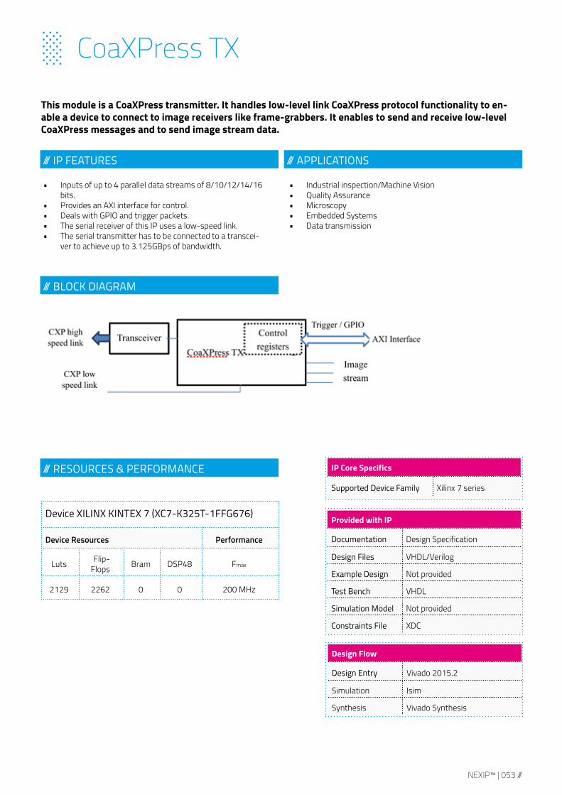
░ CoaXPress TX
This module is a CoaXPress transmitter. It handles low-level link CoaXPress protocol functionality to en-able a device to connect to image receivers like frame-grabbers. It enables to send and receive low-level CoaXPress messages and to send image stream data.
• Inputs of up to 4 parallel data streams of 8/10/12/14/16 bits.
• Provides an AXI interface for control.• Deals with GPIO and trigger packets.• The serial receiver of this IP uses a low-speed link.• The serial transmitter has to be connected to a transcei-
ver to achieve up to 3.125GBps of bandwidth.
• Industrial inspection/Machine Vision• Quality Assurance• Microscopy• Embedded Systems• Data transmission
Provided with IP
Documentation Design Specification
Design Files VHDL/Verilog
Example Design Not provided
Test Bench VHDL
Simulation Model Not provided
Constraints File XDC
Design Flow
Design Entry Vivado 2015.2
Simulation Isim
Synthesis Vivado Synthesis
IP Core Specifics
Supported Device Family Xilinx 7 series
Device XILINX KINTEX 7 (XC7-K325T-1FFG676)
Device Resources Performance
Luts Flip-Flops Bram DSP48 Fmax
2129 2262 0 0 200 MHz

/// 054 | NEXIP™
/// APPLICATIONS/// IP FEATURES
/// RESOURCES & PERFORMANCE
/// BLOCK DIAGRAM
░ CoaXPress RXThis module is a CoaXPress receiver. It handles low-level link CoaXPress protocol functionality for a host to connect to image sources such as cameras. It allows user to send and receive low-level CoaXPress mes-sages and receive image stream.
• Output of 4 parallels data stream of 8/10/12/14/16 bits. • Provides an AXI interface for control.• Deals with GPIO and trigger packets.• The serial transmitter of this IP uses a low-speed link.
The serial receiver has to be connected to a transceiver to achieve up to 3.125GBps of bandwidth.
• Industrial inspection/Machine Vision• Quality Assurance• Microscopy• Embedded Systems• Data transmission
Provided with IP
Documentation Design Specification
Design Files VHDL/Verilog
Example Design Not provided
Test Bench VHDL
Simulation Model Not provided
Constraints File XDC
Design Flow
Design Entry Vivado 2015.2
Simulation Isim
Synthesis Vivado Synthesis
IP Core Specifics
Supported Device Family Xilinx 7 series
Device XILINX KINTEX 7 (XC7-K325T-1FFG676)
Device Resources Performance
Luts Flip-Flops Bram DSP48 Fmax
1353 1294 0 0 200 MHz

NEXIP™ | 055 ///

DATA LINK

NEXIP™ | 057 ///
▌DATA LINK
> PCIe > USB 2.0, 3.0 et 3.1 (FX3) > NVMe / SSD > Fiber-optic interconnect

/// APPLICATIONS/// IP FEATURES
/// 058 | NEXIP™
/// RESOURCES & PERFORMANCE
/// BLOCK DIAGRAM
░ USB3 : Cypress FX3 Interface
• Supports FX3 32bits or 16 bits data interface.• Supports 3 different input pipes and 2 output pipes for data
flow.• Provides 4 output registers and 10 input registers for general
purposes control • Pipe buffer size configurable default to 4KB.• Output clock configurable for optimized interface timings.
This IP provides an interface to Cypress EZ-USB FX3 component. It provides, through the GPIF2 interface, read/write accesses to single registers, for system control, and to pipes interfaces, for large data transfers.
• high speed data transfer over USB3
Provided with IP
Documentation Design Specification
Validation Specification
Implementation Specification
Design Files Verilog
Example Design Provided
Test Bench VHDL
Simulation Model Not provided
Constraints File
Design Flow
Design Entry Vivado 2015.1
Simulation Isim
Synthesis Vivado Synthesis
IP Core Specifics
Supported Device Family Xilinx 7 series
Device XILINX KINTEX 7 (XC7-K325T-1FFG676)
Generic Parameter Device Resources Performance
Data bus size Clock inversion Endpoint buffer size Luts Flip-Flops Bram DSP48 Fmax
16 0 4096 515 329 0 0 100 MHz

NEXIP™ | 059 ///

MISCELLANEOUS

NEXIP™ | 061 ///
▌MISCELLANEOUS > Memory test > Master AXI Lite Intf > AXI Master Interface > Axi Lite Slave Intf > Flash SPI Controller > I2C driver
▌MOTOR CONTROL > SSI-6 > PID Controller > PWM > Sensored Brushless motor control
/// 062 | NEXIP™
/// APPLICATIONS/// IP FEATURES
/// BLOCK DIAGRAM
/// RESOURCES & PERFORMANCE
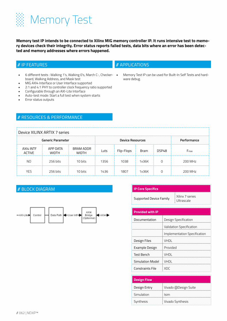
░ Memory TestMemory test IP intends to be connected to Xilinx MIG memory controller IP. It runs intensive test to memo-ry devices check their integrity. Error status reports failed tests, data bits where an error has been detec-ted and memory addresses where errors happened.
• 6 different tests : Walking 1’s, Walking 0’s, March C-, Checker-board, Walking Address, and Mask test
• MIG AXI4 Interface or User Interface supported• 2:1 and 4:1 PHY to controller clock frequency ratio supported• Configurable through an AXI-Lite Interface• Auto-test mode: Start a full test when system starts• Error status outputs
• Memory Test IP can be used for Built-In Self Tests and hard-ware debug.
Provided with IP
Documentation Design Specification
Validation Specification
Implementation Specification
Design Files VHDL
Example Design Provided
Test Bench VHDL
Simulation Model VHDL
Constraints File XDC
Design Flow
Design Entry Vivado @Design Suite
Simulation Isim
Synthesis Vivado Synthesis
IP Core Specifics
Supported Device Family Xilinx 7 seriesUltrascale
Device XILINX ARTIX 7 series
Generic Parameter Device Resources Performance
AXI4 INTF ACTIVE
APP DATA WIDTH
BRAM ADDR WIDTH Luts Flip-Flops Bram DSP48 Fmax
NO 256 bits 10 bits 1356 1038 1x36K 0 200 MHz
YES 256 bits 10 bits 1436 1807 1x36K 0 200 MHz
NEXIP™ | 063 ///
/// APPLICATIONS/// IP FEATURES
/// RESOURCES & PERFORMANCE
/// BLOCK DIAGRAM
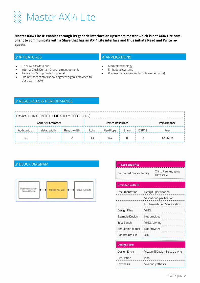
░ Master AXI4 LiteMaster AXI4 Lite IP enables through its generic interface an upstream master which is not AXI4 Lite com-pliant to communicate with a Slave that has an AXI4 Lite interface and thus initiate Read and Write re-quests.
• 32 or 64 bits data bus.• Internal Clock Domain Crossing management.• Transaction’s ID provided (optional).• End of transaction Acknowledgment signals provided to
Upstream master.
Provided with IP
Documentation Design Specification
Validation Specification
Implementation Specification
Design Files VHDL
Example Design Not provided
Test Bench VHDL/Verilog
Simulation Model Not provided
Constraints File XDC
Design Flow
Design Entry Vivado @Design Suite 2014.4
Simulation Isim
Synthesis Vivado Synthesis
IP Core Specifics
Supported Device Family Xilinx 7 series, zynq,Ultrascale
Device XILINX KINTEX 7 (XC7-K325TFFG900-2)
Generic Parameter Device Resources Performance
Addr_width data_width Resp_width Luts Flip-Flops Bram DSP48 Fmax
32 32 2 13 164 0 0 120 MHz
• Medical technology• Embedded systems• Vision enhancement (automotive or airborne)
/// 064 | NEXIP™
/// APPLICATIONS/// IP FEATURES
/// RESOURCES & PERFORMANCE
/// BLOCK DIAGRAM
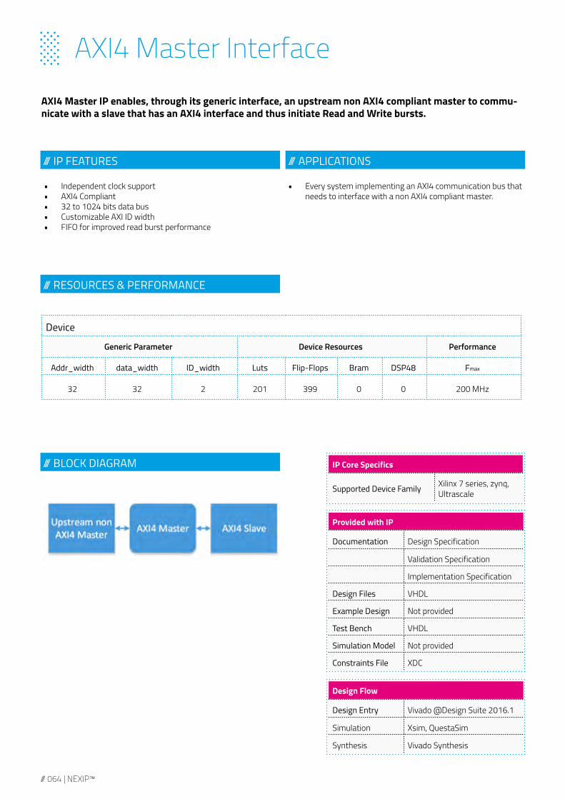
░ AXI4 Master InterfaceAXI4 Master IP enables, through its generic interface, an upstream non AXI4 compliant master to commu-nicate with a slave that has an AXI4 interface and thus initiate Read and Write bursts.
• Independent clock support• AXI4 Compliant• 32 to 1024 bits data bus• Customizable AXI ID width• FIFO for improved read burst performance
Provided with IP
Documentation Design Specification
Validation Specification
Implementation Specification
Design Files VHDL
Example Design Not provided
Test Bench VHDL
Simulation Model Not provided
Constraints File XDC
Design Flow
Design Entry Vivado @Design Suite 2016.1
Simulation Xsim, QuestaSim
Synthesis Vivado Synthesis
IP Core Specifics
Supported Device Family Xilinx 7 series, zynq,Ultrascale
Device
Generic Parameter Device Resources Performance
Addr_width data_width ID_width Luts Flip-Flops Bram DSP48 Fmax
32 32 2 201 399 0 0 200 MHz
• Every system implementing an AXI4 communication bus that needs to interface with a non AXI4 compliant master.

NEXIP™ | 065 ///
/// APPLICATIONS/// IP FEATURES
/// RESOURCES & PERFORMANCE
/// BLOCK DIAGRAM
░ AXI Lite SlaveThe IP provides a seamless interface between an AXI Lite bus system and an IP which is not natively AXI Lite compliant. It deals with clock domain crossing from AXI domain to Slave domain.
• Handles R/W registers and RO registers interface from AXI side.
• Number of registers configurable • Provides lock mechanism for exclusive accesses• Power aware with intensive automatic clock gating
• Every system implementing an AXI lite communication bus that needs to interface with a non AXI Lite compliant slave
Provided with IP
Documentation Design Specification
Validation Specification
Implementation Specification
Design Files VHDL
Example Design Not provided
Test Bench VHDL
Simulation Model Not provided
Constraints File XDC
Design Flow
Design Entry Vivado 2015.4.1
Simulation Isim
Synthesis Vivado Synthesis
IP Core Specifics
Supported Device Family Xilinx 7 seriesUltrascale
Device XILINX KINTEX 7 (XC7-K325TFFG900-2)
Generic Parameter Device Resources Performance
R/W RO Luts Flip-Flops Bram DSP48 Fmax
5 7 101 265 0 0 100 MHz

/// 066 | NEXIP™
/// APPLICATIONS/// IP FEATURES
/// RESOURCES & PERFORMANCE
/// BLOCK DIAGRAM
░ I2C Driver
I2C Driver IP delivers a generic interface for an I2C slave module. Its purpose is to provide a communication channel to an I2C module whatever the Master is. For Instance, in the Block diagram below, it interfaces an AXI4 lite Master to an I2C slave module. AXI slave and AXI Master IPs can be provided aside.
• Multi I2C Slave• START and STOP generation• Repeated START generation• Acknowledge bit generation/detection• 7 bits or 10 bits addressing• Transmission and reception FIFO size configurable ( by
default 2048 bytes deep)• Reset the communication.
Provided with IP
Documentation Design Specification
Validation Specification
Implementation Specification
Design Files VHDL
Example Design VHDL
Test Bench VHDL/Verilog
Simulation Model Verilog
Design Flow
Design Entry Vivado @Design Suite
Simulation Isim
Synthesis Vivado Synthesis
IP Core Specifics
Supported Device Family Xilinx 7 series
Device XILINX KINTEX 7 (XC7-K325T-1FFG676)
Device Resources Performance
Luts Flip-Flops Bram DSP48 Fmax
710 452 0 0 120 MHz

NEXIP™ | 067 ///
/// APPLICATIONS/// IP FEATURES
/// RESOURCES & PERFORMANCE
/// BLOCK DIAGRAM
░ Flash SPI Controller
• Support 7 Series and Ultrascale families.• SPI Single supported, Dual and Quad not supported.• Up to 256 Memory slaves.• SPI mode 0, 3 supported (mode 1, 2 are optional).• Memory Calibration, Page Program, Fast Read, Sector and
Bulk Erase user commands available.• 3 Bytes addressing mode + extender.• SPI clock dynamically controlled.• Memory automatic calibration done for Fast Read.• Possibility to stop a burst operation: Several Page Program,
Fast Read or Sector Erase operations.• Error flags available for Slave Select, Bulk Erase, Sector
Erase, Page Program and Calibration operations.• FSM state and address are available for debug.• Tested on N25Q512, N25Q256 and M25P80 memories.
Flash SPI Controller IP allows an upstream master which is not SPI compliant to communicate with one or several Flash SPI memory, initiating requests with this/these Slave(s) and thus read or store data from/to them.
• Medical Technology• Embedded Systems• Vision enhancement (automotive or airborne)
Provided with IP
Documentation Design Specification
Validation Specification
Implementation Specification
Design Files VHDL
Example Design VHDL/Verilog
Test Bench VHDL
Simulation Model Not provided
Design Flow
Design Entry Vivado @Design Suite
Simulation Isim, ModelSim
Synthesis Vivado Synthesis
IP Core Specifics
Supported Device Family Xilinx 7 seriesUltrascale
Device XILINX ULTRASCALE XCKU040
Generic Parameter Device Resources Frequency (MHz)
Device_family StartupEx Memory number Luts Flip-Flops Bram DSP48 System SPI
ULTRASCALE TRUE 1 1087 298 0 0 200 100

/// 068 | NEXIP™
/// APPLICATIONS/// IP FEATURES
/// RESOURCES & PERFORMANCE
/// BLOCK DIAGRAM
░ PID Controller
This IP is a PID controller use for any regulation.
• Data_width range from 1 to 64 bits.• Coefficients Kp, Ki and Kd.• Output limit control thanks to MAX_LIMIT and MIN_LIMIT
parameters
Provided with IP
Documentation Design Specification
Validation Specification
Implementation Specification
Design Files VHDL
Example Design Not provided
Test Bench VHDL
Simulation Model Not provided
Constraints File XDC
Design Flow
Design Entry Vivado @Design Suite
Simulation Isim
Synthesis Vivado Synthesis
IP Core Specifics
Supported Device Family All Xilinx 7 series
• Electric Motor position or speed regulation• Electric Current regulation
Device
Generic Parameter Device Resources Performance
Data width Max limit Min limit Luts Flip-Flops Bram DSP48 Fmax
14 7000 -7000 213 277 0 16 100 MHz
NEXIP™ | 069 ///
/// APPLICATIONS/// IP FEATURES
/// RESOURCES & PERFORMANCE
/// BLOCK DIAGRAM
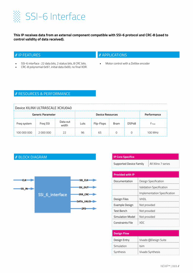
░ SSI-6 Interface
This IP receives data from an external component compatible with SSI-6 protocol and CRC-8 (used to control validity of data received).
• SSI-6 interface : 22 data bits, 2 status bits, 8 CRC bits.• CRC-8 polynomial 0x97, initial data 0x00, no final XOR.
Provided with IP
Documentation Design Specification
Validation Specification
Implementation Specification
Design Files VHDL
Example Design Not provided
Test Bench Not provided
Simulation Model Not provided
Constraints File XDC
Design Flow
Design Entry Vivado @Design Suite
Simulation Isim
Synthesis Vivado Synthesis
IP Core Specifics
Supported Device Family All Xilinx 7 series
• Motor control with a Zettlex encoder
Device XILINX ULTRASCALE XCKU040
Generic Parameter Device Resources Performance
Freq system Freq SSI Data out width Luts Flip-Flops Bram DSP48 Fmax
100 000 000 2 000 000 22 96 65 0 0 100 MHz

/// 070 | NEXIP™
/// APPLICATIONS/// IP FEATURES
/// RESOURCES & PERFORMANCE
/// BLOCK DIAGRAM
░ PWM Electric Motor Driver
This IP convert a speed setpoint into 6 PWM signals to manage a 3-phases brushless AC motor using a 6-phases driver.
• PWM frequency = Sys_freq/2000• Control of torque• Dead-time switch parameters• Pre-charged sinus LUT for PWM generation
• Electric Motor control with a PI regulation or just a speed setpoint.
Device
Generic Parameter Device Resources Performance
PWM Speed width
Nb Clock Dead time Luts Flip-Flops Bram DSP48 Fmax
14 5 659 322 0 0 100 MHz
Provided with IP
Documentation Design Specification
Validation Specification
Implementation Specification
Design Files VHDL
Example Design Not provided
Test Bench VHDL
Simulation Model Not provided
Constraints File XDC
Design Flow
Design Entry Vivado @Design Suite
Simulation Isim
Synthesis Vivado Synthesis
IP Core Specifics
Supported Device Family All Xilinx 7 series

NEXIP™ | 071 ///
/// APPLICATIONS/// IP FEATURES
/// RESOURCES & PERFORMANCE
░ Sensor brushless motor control
This IP allows to control speed or position of a brushless AC motor with sensor. The precision of the control depends on the precision of the encoder. A track mode can be set to keep heading for a define direction thanks to a gyroscope.
• High precision control• IHM to set some parameters via UART• Configurable input width• I2C interface for the gyroscope or IMU
• Motor position or speed regulation• Stabilization• Tracking
Device
Generic Parameter Device Resources Performance
Theta width
UART Baud rate Sys_clk IMU Freq Luts Flip-Flops Bram DSP48 Fmax
14 115200 100MHz 400 2300 2300 1 11 100 MHz
Provided with IP
Documentation Design Specification
Validation Specification
Implementation Specification
Design Files VHDL
Example Design Not provided
Test Bench VHDL
Simulation Model Not provided
Constraints File XDC
Design Flow
Design Entry Vivado @Design Suite
Simulation Isim
Synthesis Vivado Synthesis
IP Core Specifics
Supported Device Family Xilinx 7 series
/// BLOCK DIAGRAM

/// 072 | NEXIP™
NEXVISION in the world
HEADQUARTER
NEXVISION SASParc Swen Sud, Bât. D2 Hall D41 bd de l’océan - Impasse Paradou 13009 MARSEILLEFRANCE
Tel : (+33) 4 91 77 62 [email protected]

NEXIP™ | 073 ///
NEXVISION in the world
TRANSPORT :
AEROSPACE :
CINEMA / MEDIA / SPORT :
SECURITY / DEFENSE :
INDUSTRY :
MAIN CUSTOMERS

Related Documents