Device TC1766 Microcode V23, V24, V25, V27 Rel. 1.6, 16.07.2007 TC1766, V23, V24, V25, V27 1/12 Rel. 1.6, 16.07.2007 Flash Firmware Status Sheet This Flash Firmware Status Sheet describes the Flash properties of the devices depending on the implemented microcode version. Deviations from the current user documentation which are device step specific but not Flash firmware related are documented in the current Errata Sheet. The 1-byte microcode version number is stored at the bit locations 103-96. This byte is accessible at LDRAM address D000 000C H after each reset, and subject to be overwritten by user data at any time. The version number is defined as “Vsn”, contained in the byte as: • s = step code (highest 4 bit, hex number). A-step = 1, B-step = 2, and so on. • n = code version number (lowest 4 bit, hex number) belonging to the step (beginning with zero for every new step code). Example: V21, V23, V3A, V3F, etc Table 1 Current Documentation TC1766 User's Manual V1.1 Aug. 2005 TC1766 Data Sheet V0.7 Feb. 2007 TriCore 1 Architecture V1.3 Oct. 2005

Welcome message from author
This document is posted to help you gain knowledge. Please leave a comment to let me know what you think about it! Share it to your friends and learn new things together.
Transcript
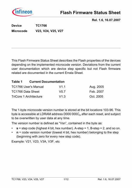
Device TC1766Microcode V23, V24, V25, V27
Rel. 1.6, 16.07.2007
Flash Firmware Status Sheet
This Flash Firmware Status Sheet describes the Flash properties of the devices depending on the implemented microcode version. Deviations from the current user documentation which are device step specific but not Flash firmware related are documented in the current Errata Sheet.
The 1-byte microcode version number is stored at the bit locations 103-96. This byte is accessible at LDRAM address D000 000CH after each reset, and subject to be overwritten by user data at any time.The version number is defined as “Vsn”, contained in the byte as:• s = step code (highest 4 bit, hex number). A-step = 1, B-step = 2, and so on.• n = code version number (lowest 4 bit, hex number) belonging to the step
(beginning with zero for every new step code).Example: V21, V23, V3A, V3F, etc
Table 1 Current DocumentationTC1766 User's Manual V1.1 Aug. 2005TC1766 Data Sheet V0.7 Feb. 2007TriCore 1 Architecture V1.3 Oct. 2005
TC1766, V23, V24, V25, V27 1/12 Rel. 1.6, 16.07.2007
Flash Firmware Status Sheet
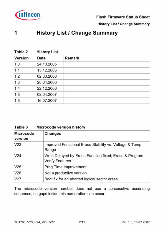
History List / Change Summary
1 History List / Change Summary
The microcode version number does not use a consecutive ascending sequence, so gaps inside this numeration can occur.
Table 2 History ListVersion Date Remark1.0 24.10.20051.1 15.12.20051.2 02.03.20061.3 28.04.20061.4 22.12.20061.5 02.04.20071.6 16.07.2007
Table 3 Microcode version historyMicrocode version
Changes
V23 Improved Functional Erase Stability vs. Voltage & Temp Range
V24 Write Delayed by Erase Function fixed; Erase & Program Verify Features
V25 Prog Time Improvement V26 Not a productive versionV27 Boot fix for an aborted logical sector erase
TC1766, V23, V24, V25, V27 2/12 Rel. 1.6, 16.07.2007
Flash Firmware Status Sheet
History List / Change Summary
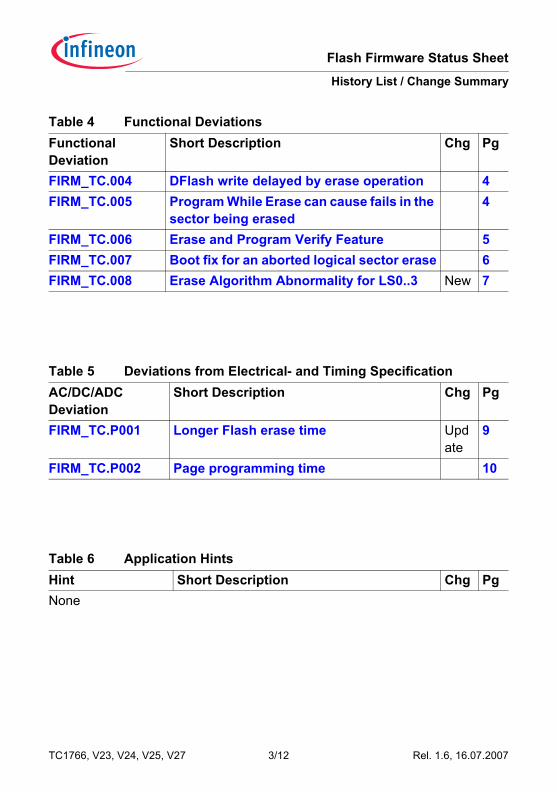
Table 4 Functional Deviations Functional Deviation
Short Description Chg Pg
FIRM_TC.004 DFlash write delayed by erase operation 4FIRM_TC.005 Program While Erase can cause fails in the
sector being erased 4
FIRM_TC.006 Erase and Program Verify Feature 5FIRM_TC.007 Boot fix for an aborted logical sector erase 6FIRM_TC.008 Erase Algorithm Abnormality for LS0..3 New 7
Table 5 Deviations from Electrical- and Timing Specification AC/DC/ADC Deviation
Short Description Chg Pg
FIRM_TC.P001 Longer Flash erase time Update
9
FIRM_TC.P002 Page programming time 10
Table 6 Application Hints Hint Short Description Chg PgNone
TC1766, V23, V24, V25, V27 3/12 Rel. 1.6, 16.07.2007
Flash Firmware Status Sheet
Functional Deviations
2 Functional Deviations
FIRM_TC.004 DFlash write delayed by erase operation
In case of an ongoing erase operation to one DFlash bank, any program request to the alternate DFlash bank will be delayed until the ongoing erase operation is fully completed. This behaviour is due to a Flash microcode issue and does not affect in any other way the Flash functionality or reliability.This erratum is valid for microcode <= V23.
WorkaroundNone.
FIRM_TC.005 Program While Erase can cause fails in the sector being erased
V24 and V25 are affected by this functional bug:Per call of a `Program while Erase` (Erase Suspend Feature) the following errors may be visible after the suspended erase is terminated in the erased sector:• either 1 page is not properly erased. This error is oftenly detectable by
reading the sector (some cells in the page read 1) but also some hard to detect weak 0 bits might be generated.
• or FSR.VER might show up: This error flag indicates that some overerased bits inside one page of the erased sector remained unrecovered (this overerased state is not customer-detectable, e.g. it will read 0 as expected) and can cause subsequent program operations to the erased sector to be unsuccessfull, (i.e.FSR.VER can appear again after programming a page (Prog Verify Fault) and the bits intented to be programmed might read 0). This state can only be left by an (successfull) re-erase.
The program result of the `program while erase` itself is not affected and will be valid.
TC1766, V23, V24, V25, V27 4/12 Rel. 1.6, 16.07.2007
Flash Firmware Status Sheet
Functional Deviations
Workaround1. re-erase a sector if the program while erase became necessary (until the
erase process was executed without any program while erase call).2. do not use Program while Erase
FIRM_TC.006 Erase and Program Verify Feature
Starting microcode V24, any internal errors detectable by the FSI state machine during erase sector or program page sequences will be indicated by activation of the FSR.VER bit before busy status is deactivated. FSR.VER errors will appear typically if operations are carried out violating device specs (exceeding endurance, operating temperature, supply voltages). FSR.VER can be indicated in seldom cases in absense of functional or reliability problems. Always consider that even if a VER would indicate a severe problem, it is usually not reasonable to stop an application in the field, but wait for functional consequences to show up.
RecommendationsThese recommendations are intended for optimization of functional safety applying the current generation of the VER feature (optional to customer application).• Recommended action for erase-VER event in field / end of line erase:
a) Immediate clear status, to catch other successive events and distinguish from prog-VER
b) Re-erase until VER disappears (max up to 3 times in sequence; afterwards ignore), but take special care to fullfill operating conditions (total sector endurance, voltage, frequency, temperature not exceeded).
c) Regardless from VER: Infineon recommends to apply, in case of "end of line" flashing or firmware update, a tight-0 check by SBE counting (or preferably a tight 0+1 check for the whole sector after sector is programmed) to determine ECC off fail rate: if single bit error (SBE) count is below 10 per sector, the risk of an incorrigible double bit error (DBE) throughout retention / further operating life is considered still negligible.
• Recommended action for prog-VER event in field / end of line programming:
TC1766, V23, V24, V25, V27 5/12 Rel. 1.6, 16.07.2007
Flash Firmware Status Sheet
Functional Deviations
a) Immediate clear status, to catch other successive events and distinguish from erase-VER
b) Never reprogram the same page (disturb budget violation) without erasec) Count VER occurrences for each individual sector since last erase (in
SRAM in volatile manner after each powerup). Up to three VER events occuring in a sector are tolerable, but take special care to fullfill operating conditions (total sector endurance, voltage, frequency, temperature not exceeded).
d) Regardless from VER: Infineon recommends to apply in case of "end of line" flashing or firmware update a tight 0+1 check (SBE event counting) for the written page, or preferably a tight 0+1 check for the whole sector, after sector is programmed: if single bit error (SBE) count is below 10 per sector, the risk of an incorrigible double bit error (DBE) throughout retention / further operating life is considered still negligible.
e) If the first program into a freshly erased sector shows prog-VER, preferably reerase and reprogram the sector (reerase no more than once in case of such prog-VER). Make sure not to program into sectors where erase operation was aborted (a prog-VER will be indicated when programming to an "aborted erase" sector left in overerase) and take special care to fullfill operating conditions.
FIRM_TC.007 Boot fix for an aborted logical sector erase
In case of an aborted logical or physical sector erase, cells might be in an over-erased state. As the presence of a partially erased / over-erased state of the flash is not reliably detectable by the user, a reerase is mandatory whenever an erase abortion cannot be excluded.
Please also refer to the application hint: Flash_TC.H005In case of an aborted logical sector erase other logical sectors may become unreadable. As a consequence the boot code or alternate boot info might be unreadable and the device isn’t booting customer code anymore.
TC1766, V23, V24, V25, V27 6/12 Rel. 1.6, 16.07.2007
Flash Firmware Status Sheet
Functional Deviations
Starting with uCode v27 the following functional enhancement will help to keep the customer boot code accessible:
- an aborted logical sector erase will be detected after reset- in presence of over-erased cells the affected sector will be fully programmed. The flash boot time will be considerably (<10ms) prolonged in this case- the ’program all’ functionality to an over-erased sector allows to recover the readability of the remaining logical sectors- the ’fixed’ logical sector will be read as all ’1’ afterwards
The FSR.VER bit will flag the detection of an aborted sector erase and it’s recovery or indicate an endangered system integrity. This flag can be reset by the clear status command.
WorkaroundNone
FIRM_TC.008 Erase Algorithm Abnormality for LS0..3
V25 microcode is affected by the following functional bug: over-erase algorithm for erase logical sectors 0..3 applies erroneously erase verify and soft-programming substeps to extended memory range (may even affect neighboring sectors).The consequences are:• the logical sector to be erased will always be physically erased
unnecessarily strong. This state will be recovered by the soft-programming step, but erase time is prolonged and in LS0..3 in seldom cases cell abnormalities can be emphasized/stimulated that cause up to 31 (bitline-oriented, e.g. offset address is 100H) single bit errors reading 1 (in an ECC correctable way) in the erased logical sector accompanied with FSR.VER indication.
• neighboring sectors will not be unintentionally erased, but may be impacted by disturb (zeroes might get slightly weaker) and additional soft-
TC1766, V23, V24, V25, V27 7/12 Rel. 1.6, 16.07.2007
Flash Firmware Status Sheet
Functional Deviations
programming resulting in potential single bit errors (SBE). The potentially SBE-impacted area for logical sectors 0 to 3 is starting at next logical sectors address SA+4000H (i.e. 004000H, 008000H, 00C000H, 010000H) and is 1C000H wide (because erroneously the size of the whole physical sector 20000H is applied instead of the logical sector's size 4000H).
WorkaroundEither:• Do not use logical sector erase LS0..3 (but physical sector erase instead),
if applicable.• Disregard VER & tolerate SBE state, if less than 10 SBEs after update.
TC1766, V23, V24, V25, V27 8/12 Rel. 1.6, 16.07.2007
Flash Firmware Status Sheet
Deviations from Electrical- and Timing Specification
3 Deviations from Electrical- and Timing Specification
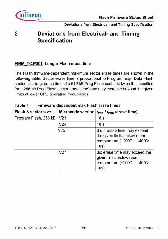
FIRM_TC.P001 Longer Flash erase time
The Flash firmware-dependent maximum sector erase times are shown in the following table. Sector erase time is proportional to Program resp. Data Flash sector size (e.g. erase time of a 512 kB Prog Flash sector is twice the specified for a 256 kB Prog Flash sector erase time) and may increase beyond the given limits at lower CPU operating frequencies.
Table 7 Firmware dependent max Flash erase times Flash & sector size Microcode version tERP / tERD (erase time)Program Flash, 256 kB V23 18 s
V24 18 sV25 8 s1); erase time may exceed
the given limits below room temperature (+20°C ... -40°C: 10s)
V27 8s; erase time may exceed the given limits below room temperature (+20°C ... -40°C: 10s)
TC1766, V23, V24, V25, V27 9/12 Rel. 1.6, 16.07.2007
Flash Firmware Status Sheet
Deviations from Electrical- and Timing Specification
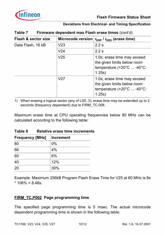
Maximum erase time at CPU operating frequencies below 80 MHz can be calculated according to the following table:
Example: Maximum 256kB Program Flash Erase Time for V25 at 60 MHz is 8s * 106% = 8.48s.
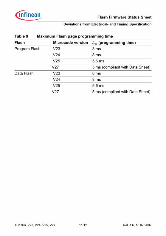
FIRM_TC.P002 Page programming time
The specified page programming time is 5 msec. The actual microcode dependent programming time is shown in the following table:
Data Flash, 16 kB V23 2.2 s V24 2.2 s V25 1.0s; erase time may exceed
the given limits below room temperature (+20°C ... -40°C: 1.25s)
V27 1.0s; erase time may exceed the given limits below room temperature (+20°C ... -40°C: 1.25s)
1) When erasing a logical sector (any of LS0..3), erase time may be extended up to 2 seconds (frequency dependent) due to FIRM_TC.008.
Table 8 Relative erase time increments Frequency [MHz] Increment80 0%66 4%60 6%40 12%20 30%
Table 7 Firmware dependent max Flash erase times (cont’d) Flash & sector size Microcode version tERP / tERD (erase time)
TC1766, V23, V24, V25, V27 10/12 Rel. 1.6, 16.07.2007
Flash Firmware Status Sheet
Deviations from Electrical- and Timing Specification
Table 9 Maximum Flash page programming timeFlash Microcode version tPR (programming time)Program Flash V23 8 ms
V24 8 ms V25 5.6 msV27 5 ms (compliant with Data Sheet)
Data Flash
V23 8 ms V24 8 ms V25 5.6 msV27 5 ms (compliant with Data Sheet)
TC1766, V23, V24, V25, V27 11/12 Rel. 1.6, 16.07.2007
Flash Firmware Status Sheet
Application Hints
4 Application HintsNone.
TC1766, V23, V24, V25, V27 12/12 Rel. 1.6, 16.07.2007
Related Documents