ARL-TR-7913 ● DEC 2016 US Army Research Laboratory Fabrication and Characterization of Vertical Gallium Nitride Power Schottky Diodes on Bulk GaN Substrates FY2016 by Bryan H Zhao, Michael A Derenge, Milena B Graziano, and Randy P Tompkins Approved for public release; distribution unlimited.

Welcome message from author
This document is posted to help you gain knowledge. Please leave a comment to let me know what you think about it! Share it to your friends and learn new things together.
Transcript

ARL-TR-7913 ● DEC 2016
US Army Research Laboratory
Fabrication and Characterization of Vertical Gallium Nitride Power Schottky Diodes on Bulk GaN Substrates FY2016
by Bryan H Zhao, Michael A Derenge, Milena B Graziano, and Randy P Tompkins Approved for public release; distribution unlimited.

NOTICES
Disclaimers
The findings in this report are not to be construed as an official Department of the Army position unless so designated by other authorized documents.
Citation of manufacturer’s or trade names does not constitute an official endorsement or approval of the use thereof.
Destroy this report when it is no longer needed. Do not return it to the originator.

ARL-TR-7913 ● DEC 2016
US Army Research Laboratory
Fabrication and Characterization of Vertical Gallium Nitride Power Schottky Diodes on Bulk GaN Substrates FY2016
by Bryan H Zhao, Michael A Derenge, Milena B Graziano, and Randy P Tompkins Sensors and Electron Devices Directorate, ARL Approved for public release; distribution unlimited.

ii
REPORT DOCUMENTATION PAGE Form Approved OMB No. 0704-0188
Public reporting burden for this collection of information is estimated to average 1 hour per response, including the time for reviewing instructions, searching existing data sources, gathering and maintaining the data needed, and completing and reviewing the collection information. Send comments regarding this burden estimate or any other aspect of this collection of information, including suggestions for reducing the burden, to Department of Defense, Washington Headquarters Services, Directorate for Information Operations and Reports (0704-0188), 1215 Jefferson Davis Highway, Suite 1204, Arlington, VA 22202-4302. Respondents should be aware that notwithstanding any other provision of law, no person shall be subject to any penalty for failing to comply with a collection of information if it does not display a currently valid OMB control number. PLEASE DO NOT RETURN YOUR FORM TO THE ABOVE ADDRESS.
1. REPORT DATE (DD-MM-YYYY)
December 2016 2. REPORT TYPE
Technical Report 3. DATES COVERED (From - To)
4. TITLE AND SUBTITLE
Fabrication and Characterization of Vertical Gallium Nitride Power Schottky Diodes on Bulk GaN Substrates FY2016
5a. CONTRACT NUMBER
5b. GRANT NUMBER
5c. PROGRAM ELEMENT NUMBER
6. AUTHOR(S)
Bryan H Zhao, Michael A Derenge, Milena B Graziano, and Randy P Tompkins 5d. PROJECT NUMBER
5e. TASK NUMBER
5f. WORK UNIT NUMBER
7. PERFORMING ORGANIZATION NAME(S) AND ADDRESS(ES)
US Army Research Laboratory ATTN: RDRL-SED-E 2800 Powder Mill Road Adelphi, MD 20783-1138
8. PERFORMING ORGANIZATION REPORT NUMBER
ARL-TR-7913
9. SPONSORING/MONITORING AGENCY NAME(S) AND ADDRESS(ES)
10. SPONSOR/MONITOR'S ACRONYM(S)
11. SPONSOR/MONITOR'S REPORT NUMBER(S)
12. DISTRIBUTION/AVAILABILITY STATEMENT
Approved for public release; distribution unlimited.
13. SUPPLEMENTARY NOTES 14. ABSTRACT
In this technical report, we report recent (FY2016) progress on the vertical Schottky diodes (SDs) on a bulk gallium nitride (GaN) substrate. The newly obtained functionality of the Micromanipulator P200L Semiautomatic Probing Station coupled with our existing Agilent 4155C Semiconductor Parameter Analyzer is also summarized. Vertical GaN SDs were fabricated on a true bulk single crystal GaN substrate grown using the ammonothermal growth technique. To investigate the electrical performance of the SDs as a function of diode size, circular diodes ranging from 50 to 300 µm in diameter were fabricated and tested. Forward I-V results suggest that the sample has high resistivity as no forward conduction was observed for all devices tested. Additionally, results show variation in the diode breakdown voltage with diode size, but no clear trend between breakdown voltage and diode size was observed.
15. SUBJECT TERMS
gallium nitride, Schottky diode, ammonothermal, I-V curve measurements, substrate
16. SECURITY CLASSIFICATION OF: 17. LIMITATION OF ABSTRACT
UU
18. NUMBER OF PAGES
20
19a. NAME OF RESPONSIBLE PERSON
Randy P Tompkins a. REPORT
Unclassified b. ABSTRACT
Unclassified c. THIS PAGE
Unclassified 19b. TELEPHONE NUMBER (Include area code)
(301) 394-0015 Standard Form 298 (Rev. 8/98) Prescribed by ANSI Std. Z39.18

Approved for public release; distribution unlimited. iii
Contents
List of Figures iv
List of Tables iv
1. Background 1
2. Micromanipulator P200L Semiautomatic Probing Station 2
3. Experiment 3
4. Results 6
5. Conclusion 9
6. References 11
List of Symbols, Abbreviations, and Acronyms 12
Distribution List 13

Approved for public release; distribution unlimited. iv
List of Figures
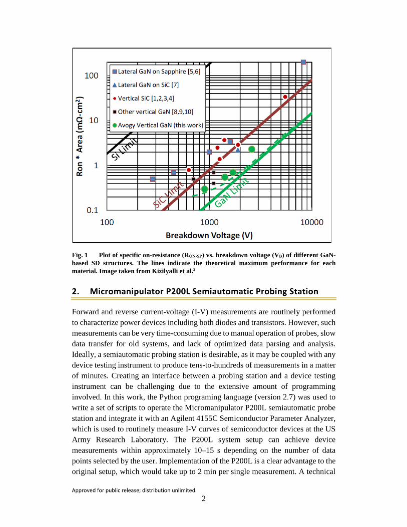
Fig. 1 Plot of specific on resistance (RON-SP) versus breakdown voltage (VB) of different GaN-based SD structures. The lines indicate the theoretical maximum performance for each material. Image taken from Ref [2]. ..2
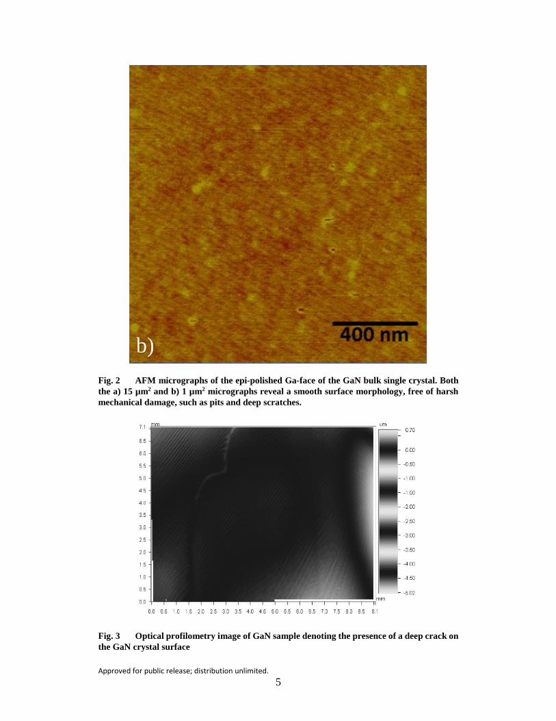
Fig. 2 AFM micrographs of the epi-polished Ga-face of the GaN bulk single crystal. Both the a) 15 µm2 and b) 1 µm2 micrographs reveal a smooth surface morphology, free of harsh mechanical damage, such as pits and deep scratches..................................................................................5
Fig. 3 Optical profilometry image of GaN sample denoting the presence of a deep crack on the GaN crystal surface ...................................................5
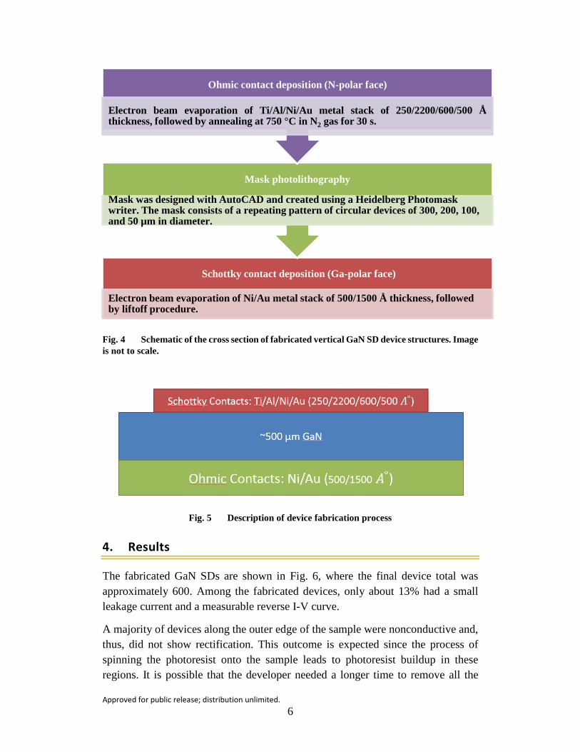
Fig. 4 Schematic of the cross-section of fabricated vertical GaN SD device structures. Image is not to scale. ............................................................6
Fig. 5 Description of device fabrication process ..............................................6
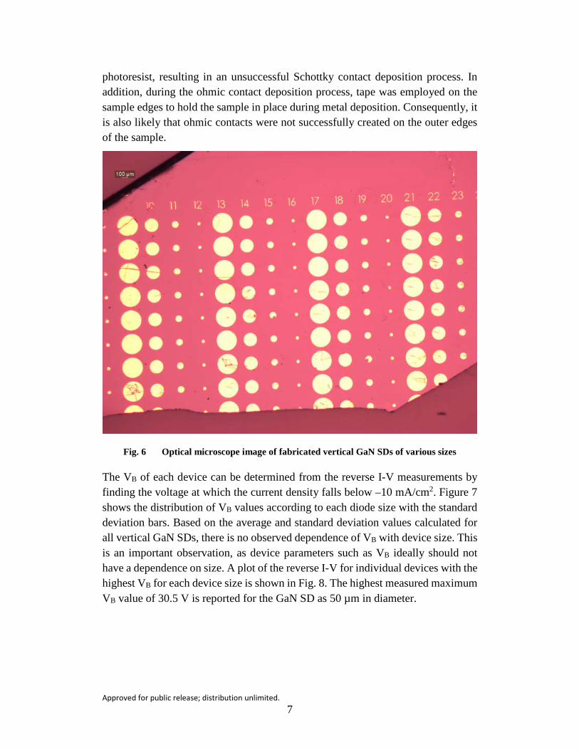
Fig. 6 Optical microscope image of fabricated vertical GaN SDs of various sizes ........................................................................................................7
Fig. 7 GaN SD device size versus average breakdown voltage. Error bars indicate one standard deviation. .............................................................8
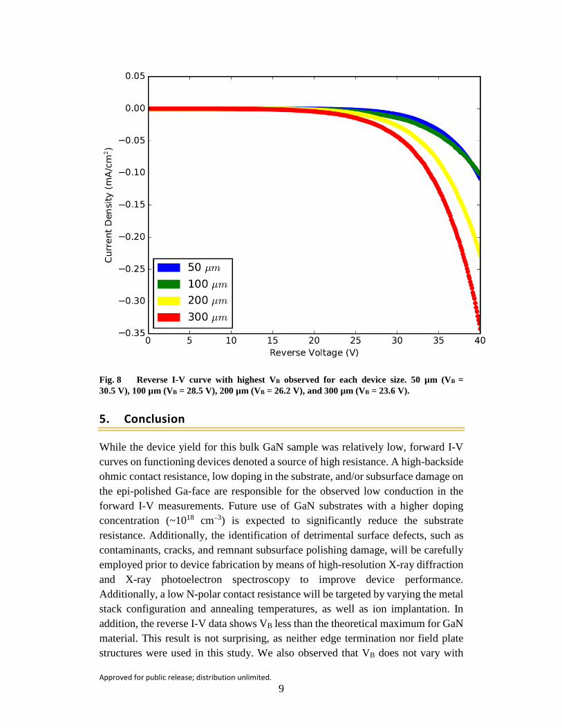
Fig. 8 Reverse I-V curve with highest (VB) observed for each device size. 50 µm (VB = 30.5 V), 100 µm (VB = 28.5 V), 200 µm (VB = 26.2 V), and 300 µm (VB = 23.6 V). ...........................................................................9
List of Tables
Table 1 Comparison of material properties between GaN, Si and SiC...............1

Approved for public release; distribution unlimited. 1
1. Introduction
Gallium nitride (GaN) is a promising material for the development of high-power electronic devices due to its high-breakdown field and high-electron mobility (Table 1). These parameters influence the Baliga’s figure of merit (BFOM) for power electronics, expressed in Eq. 1:
𝐁𝐁𝐁𝐁𝐁𝐁𝐁𝐁 = 𝛆𝛆 ∗ 𝛍𝛍 ∗ 𝐄𝐄C𝟑𝟑 , (1)
where 𝛆𝛆 is the dielectric constant, 𝛍𝛍 is the electron mobility, and 𝐄𝐄C is the critical electric field.1 With the reported critical electric field of GaN ranging from 3.3 to 3.75 mV/cm, GaN’s BFOM is several times larger than that of silicon (Si) and silicon carbide (SiC) (Fig. 1).2
Historically, the lack of lattice-matched substrates for nitride epitaxy has resulted in GaN-based device development on foreign substrates such as sapphire, SiC, and Si. The large lattice mismatch in these systems leads to highly defective heterostructures (108–1010 dislocations/cm2), which can ultimately limit device performance.3 Recent advances in GaN bulk crystal growth have increased the availability and use of high-quality native substrates, demonstrating an ideal route for achieving GaN-based device structures with low-threading dislocation density and low-impurity incorporation. Thus, it is expected that Schottky diodes (SDs) fabricated on bulk GaN single crystals will have improved device reliability and larger breakdown voltages compared to devices on heteroepitaxial GaN.
Table 1 Comparison of material properties between GaN, Si, and SiC4
Approved for public release; distribution unlimited. 2
Fig. 1 Plot of specific on-resistance (RON-SP) vs. breakdown voltage (VB) of different GaN-based SD structures. The lines indicate the theoretical maximum performance for each material. Image taken from Kizilyalli et al.2
2. Micromanipulator P200L Semiautomatic Probing Station
Forward and reverse current-voltage (I-V) measurements are routinely performed to characterize power devices including both diodes and transistors. However, such measurements can be very time-consuming due to manual operation of probes, slow data transfer for old systems, and lack of optimized data parsing and analysis. Ideally, a semiautomatic probing station is desirable, as it may be coupled with any device testing instrument to produce tens-to-hundreds of measurements in a matter of minutes. Creating an interface between a probing station and a device testing instrument can be challenging due to the extensive amount of programming involved. In this work, the Python programing language (version 2.7) was used to write a set of scripts to operate the Micromanipulator P200L semiautomatic probe station and integrate it with an Agilent 4155C Semiconductor Parameter Analyzer, which is used to routinely measure I-V curves of semiconductor devices at the US Army Research Laboratory. The P200L system setup can achieve device measurements within approximately 10–15 s depending on the number of data points selected by the user. Implementation of the P200L is a clear advantage to the original setup, which would take up to 2 min per single measurement. A technical

Approved for public release; distribution unlimited. 3
report on the programming aspects of the P200L semiautomatic probing station that will include the source code is currently in preparation. In this project, we demonstrate the capability of the semiautomatic probe system, and we report on the I-V curve measurements taken on the vertical GaN SDs fabricated on a bulk GaN substrate.
3. Experiment
In this work, vertical SD structures were prepared using a 500-µm-thick ammonothermally grown GaN bulk crystal provided by a commercial vendor. The substrate was cut from a (0001)-oriented crystal boule and was double-side mechanically polished. Chemical-mechanical polishing was further employed on the Ga-face to reduce gross mechanical damage from the boule sawing and mechanical polishing processing steps. As revealed by atomic force microscopy (AFM) imaging, the epi-polished Ga-face revealed a clear bilayer step morphology with a root mean square roughness of 0.27 ±0.07 nm (Fig. 2).
Optical profilometry measurements revealed the presence of a large crack through the entire sample (Fig. 3). At present, the origin of the crack is unknown. Devices reported in this technical report are not located on the crack.
Following materials characterization, vertical GaN SDs (Fig. 4) were fabricated following a series of steps, which are summarized in Fig. 5. The first step in the fabrication process for vertical SDs involved creating ohmic contacts on the N-polar face (backside) of the GaN sample by depositing a titanium/aluminum/nickel/gold (Ti/Al/Ni/Au) (250/2200/600/500 Å) metal stack using electron beam evaporation. The contacts were then annealed at 750 °C in N2 gas for 30 s using rapid thermal annealing.
Next, photoresist was spun onto the Ga-face at 2000 rpm to give a resist thickness of approximately 2 µm. Following resist exposure, a soft bake was performed at 95 °C for 60 s on a hot plate. The resist was then exposed to UV light for 4.2 s while in contact with the mask. To perform image reversal, the exposed resist was baked at 105 °C for 30 s on a hot plate and subsequently flood exposed for 8 s. After flood exposure, the sample was developed for 60 s in an AZ300 Metal Ion Free developer. Following development, the sample was placed in an oxygen plasma for 5 min to remove residual photoresist, a process referred to as descuming. The sample was then etched in hydrochloric acid for 30 s, rinsed with deionized water, and blown dry in nitrogen gas. Front-side Schottky contacts were created by depositing a Ni/Au (500/1500 Å) metal stack using electron beam evaporation. Following metal evaporation, we performed a liftoff procedure consisting of placing the sample in acetone for about 2 h until the metal is easily removed in regions that have
Approved for public release; distribution unlimited. 4
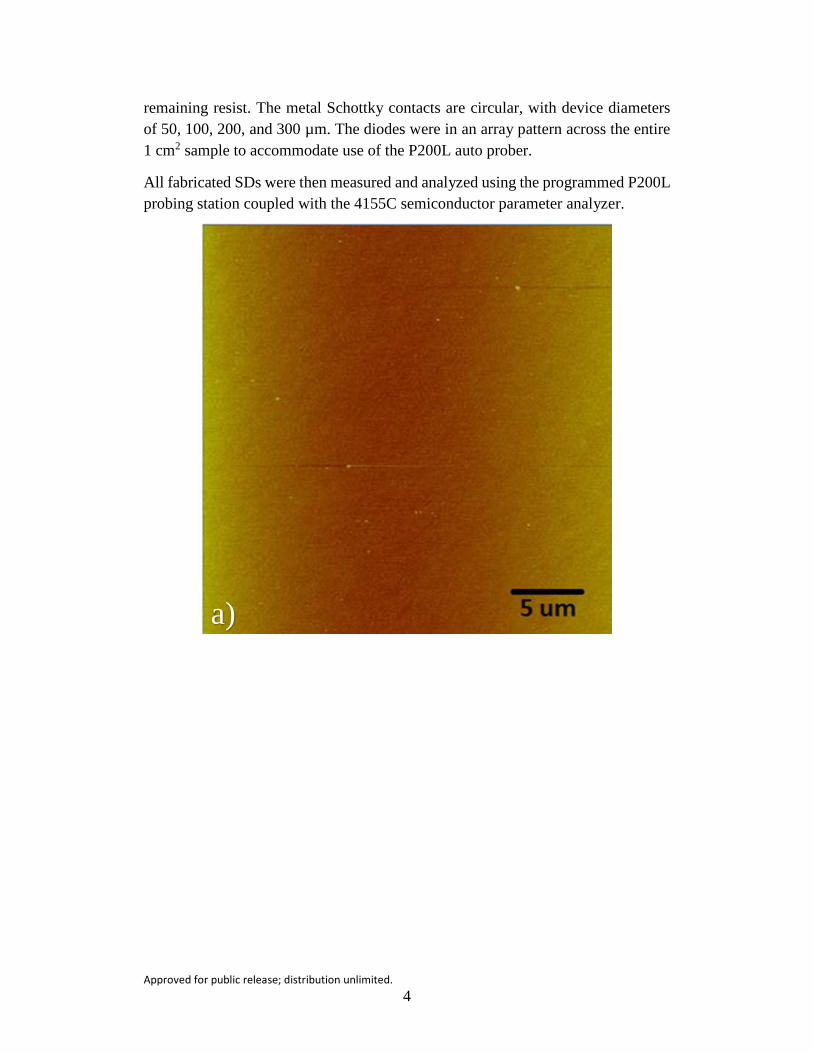
remaining resist. The metal Schottky contacts are circular, with device diameters of 50, 100, 200, and 300 µm. The diodes were in an array pattern across the entire 1 cm2 sample to accommodate use of the P200L auto prober.
All fabricated SDs were then measured and analyzed using the programmed P200L probing station coupled with the 4155C semiconductor parameter analyzer.
a)
Approved for public release; distribution unlimited. 5
Fig. 2 AFM micrographs of the epi-polished Ga-face of the GaN bulk single crystal. Both the a) 15 µm2 and b) 1 µm2 micrographs reveal a smooth surface morphology, free of harsh mechanical damage, such as pits and deep scratches.
Fig. 3 Optical profilometry image of GaN sample denoting the presence of a deep crack on the GaN crystal surface
b)
Approved for public release; distribution unlimited. 6
Fig. 4 Schematic of the cross section of fabricated vertical GaN SD device structures. Image is not to scale.
Fig. 5 Description of device fabrication process
4. Results
The fabricated GaN SDs are shown in Fig. 6, where the final device total was approximately 600. Among the fabricated devices, only about 13% had a small leakage current and a measurable reverse I-V curve.
A majority of devices along the outer edge of the sample were nonconductive and, thus, did not show rectification. This outcome is expected since the process of spinning the photoresist onto the sample leads to photoresist buildup in these regions. It is possible that the developer needed a longer time to remove all the
Schottky contact deposition (Ga-polar face)
Electron beam evaporation of Ni/Au metal stack of 500/1500 Å thickness, followed by liftoff procedure.
Mask photolithography
Mask was designed with AutoCAD and created using a Heidelberg Photomask writer. The mask consists of a repeating pattern of circular devices of 300, 200, 100, and 50 µm in diameter.
Ohmic contact deposition (N-polar face)
Electron beam evaporation of Ti/Al/Ni/Au metal stack of 250/2200/600/500 Åthickness, followed by annealing at 750 °C in N2 gas for 30 s.
Approved for public release; distribution unlimited. 7
photoresist, resulting in an unsuccessful Schottky contact deposition process. In addition, during the ohmic contact deposition process, tape was employed on the sample edges to hold the sample in place during metal deposition. Consequently, it is also likely that ohmic contacts were not successfully created on the outer edges of the sample.
Fig. 6 Optical microscope image of fabricated vertical GaN SDs of various sizes
The VB of each device can be determined from the reverse I-V measurements by finding the voltage at which the current density falls below –10 mA/cm2. Figure 7 shows the distribution of VB values according to each diode size with the standard deviation bars. Based on the average and standard deviation values calculated for all vertical GaN SDs, there is no observed dependence of VB with device size. This is an important observation, as device parameters such as VB ideally should not have a dependence on size. A plot of the reverse I-V for individual devices with the highest VB for each device size is shown in Fig. 8. The highest measured maximum VB value of 30.5 V is reported for the GaN SD as 50 µm in diameter.

Approved for public release; distribution unlimited. 8
Fig. 7 GaN SD device size vs. average breakdown voltage. Error bars indicate one standard deviation.
Approved for public release; distribution unlimited. 9
Fig. 8 Reverse I-V curve with highest VB observed for each device size. 50 µm (VB = 30.5 V), 100 µm (VB = 28.5 V), 200 µm (VB = 26.2 V), and 300 µm (VB = 23.6 V).
5. Conclusion
While the device yield for this bulk GaN sample was relatively low, forward I-V curves on functioning devices denoted a source of high resistance. A high-backside ohmic contact resistance, low doping in the substrate, and/or subsurface damage on the epi-polished Ga-face are responsible for the observed low conduction in the forward I-V measurements. Future use of GaN substrates with a higher doping concentration (~1018 cm–3) is expected to significantly reduce the substrate resistance. Additionally, the identification of detrimental surface defects, such as contaminants, cracks, and remnant subsurface polishing damage, will be carefully employed prior to device fabrication by means of high-resolution X-ray diffraction and X-ray photoelectron spectroscopy to improve device performance. Additionally, a low N-polar contact resistance will be targeted by varying the metal stack configuration and annealing temperatures, as well as ion implantation. In addition, the reverse I-V data shows VB less than the theoretical maximum for GaN material. This result is not surprising, as neither edge termination nor field plate structures were used in this study. We also observed that VB does not vary with

Approved for public release; distribution unlimited. 10
device size—an important observation, as device properties should not vary with size across the wafer. It is expected that VB will increase with implementation and optimization of such structures as guard rings and/or field plates. All proposed changes are expected to significantly improve the VB of vertical GaN SD structures.
Approved for public release; distribution unlimited. 11
6. References
1. Baliga BJ. Power semiconductor device figure of merit for high-frequency applications. IEEE Electron Device Letters. 1989;10(10):455–457.
2. Kizilyalli IC, Edwards A, Bour D, Shah H, Nie H, Disney D. High2Power Today; (Mar 2013).
3. Paskova T, Hanser DA, Evans KR. Proceedings of the IEEE 2010;98(7):1324–1338.
4. Microsemi. Gallium nitride (GaN) versus silicon carbide (SiC) in the high frequency (RF) and power switching applications; [accessed 2016 June 30]. http://www.richardsonrfpd.com/resources/RellDocuments/SYS_26/Microsemi-A-Comparison-of-Gallium-Nitride-Versus-Silicon-Carbide.pdf.

Approved for public release; distribution unlimited. 12
List of Symbols, Abbreviations, and Acronyms
Å angstroms
AFM atomic force microscopy
Al aluminum
Au gold
BFPM Baliga’s figure of merit
FY16 fiscal year 2016
GaN gallium nitride
HCl hydrochloric acid
I-V current-voltage
µm microns
Ni nickel
Ron-sp specific on-resistance
SD Schottky diode
Si Silicon
SiC silicon carbide
Ti titanium
UV ultraviolet
VB breakdown voltage

Approved for public release; distribution unlimited. 13
1 DEFENSE TECH INFO CTR (PDF) DTIC OCA 2 US ARMY RSRCH LAB (PDF) IMAL HRA MAIL & RECORDS MGMT RDRL CIO L TECHL LIB 1 GOVT PRNTG OFC (PDF) A MALHOTRA 7 US ARMY RSRCH LAB (PDF) RDRL SE RL M DERENGE RDRL SED E CM WAITS KA JONES M GRAZIANO P BARNES R TOMPKINS RDRL SEE E W ZHOU

Approved for public release; distribution unlimited. 14
INTENTIONALLY LEFT BLANK.
Related Documents