IEEE TRANSACTIONS ON ELECTRON DEVICES, VOL. 63, NO. 4, APRIL 2016 1587 Vertical LEDs on Rigid and Flexible Substrates Using GaN-on-Si Epilayers and Au-Free Bonding Xinbo Zou, Member, IEEE, Xu Zhang, Wing Cheung Chong, Chak Wah Tang, and Kei May Lau, Fellow, IEEE Abstract—Vertical-injection light-emitting diodes (VLEDs) were fabricated and demonstrated on mechanically rigid and flexible substrates using GaN-on-Si epilayers and a cost-effective Au-free Cu/Sn bonding method. With a mirror layer between the VLEDs and the receptor Si(100) carrier, 500 μm × 500 μm VLEDs emit up to 134-mW optical power at a drive current of 300 mA. The peak wall-plug efficiency was 23% at 1-A/cm 2 current injection density. Due to excellent heat dissipation of the metal and Si carrier, the VLED junction temperature was measured to be only 47.5 °C at a working current density of 350 mA/mm 2 and increased by 0.27 °C per 1-mA current increment. After release from the rigid substrate, the 40-μm-thick Cu/Sn/Cu bonding layer can also work as a handling substrate to paste LED thin films onto flexible substrates, including plastic and paper. The self-contained VLED structure exhibited the original I –V characteristics and high brightness on various substrates. The results attest to the feasibility of using GaN-on-Si epilayers and Cu/Sn/Cu bonding for a wide range of applications, including low-cost solid-state lighting and flexible illuminations. Index Terms—Au-free bonding, GaN LEDs grown on Si, rigid and flexible substrates, vertical LEDs. I. I NTRODUCTION G aN/InGaN light-emitting diodes (LEDs), with their high internal quantum efficiency, low-power consump- tion, and long lifetime, are widely used in applications, such as indication lights, display, general illumination, and so on [1]–[4]. In the last decade, to lower the cost of LED manufacturing, the growth technology of GaN on inexpensive and large area Si substrates has been developed [5]–[8]. In spite of the large lattice constant and thermal expan- sion mismatch between GaN and Si, great advances have been achieved in growing high-quality GaN-based LEDs on Si substrates [6], [9]. Considering the light-absorptive properties of a Si substrate, it is preferred to fabricate vertical-injection LEDs (VLEDs) with light-reflective mirrors and/or a roughened surface to significantly increase light extraction [10]–[13]. To fabricate VLEDs, a key step is to bond Manuscript received November 2, 2015; accepted February 3, 2016. Date of publication February 18, 2016; date of current version March 22, 2016. This work was supported by the Research Grants Council within the Theme-Based Research Scheme, Hong Kong, under Grant T23-612/12-R. The review of this paper was arranged by Editor J. Huang. X. Zou and K. M. Lau are with the Department of Electronic and Computer Engineering, The Hong Kong University of Science and Technology (HKUST), Hong Kong, and also with the HKUST Jockey Club Institute for Advanced Study, HKUST, Hong Kong (e-mail: [email protected]; [email protected]). X. Zhang, W. C. Chong, and C. W. Tang are with the Department of Electronic and Computer Engineering, The Hong Kong University of Science and Technology, Hong Kong (e-mail: [email protected]; [email protected]; [email protected]). Color versions of one or more of the figures in this paper are available online at http://ieeexplore.ieee.org. Digital Object Identifier 10.1109/TED.2016.2526685 LEDs onto a carrier substrate using a metal-based soldering layer. Au-based metal combinations, such as Au/In [11], Ti/Au [14], and Au/Sn [15], are commonly used as the bonding layers for transferring the LED thin film onto a Si carrier. Despite the attractive performance demonstrated by VLEDs using Au-based bonding layers, the high cost of depositing micrometer-thick Au is an important obstacle for the devel- opment of cost-effective solid-state lighting. Furthermore, the use of Au is not compatible in a Si production line. Thus, in recent years, there has been a trend to develop Au-free metallization schemes to allow the fabrication of GaN-on-Si devices, e.g., the development of a high electron mobility transistor [16]–[18] in standard CMOS lines to make full use of production facilities and to further lower production cost. Flexible LEDs (FLEDs) made of III-N materials [19]–[22] can be an alternative to organic LEDs in applications, such as deformable displays, wearable electronics, and biomedi- cine (e.g., optical-stimulation cochlear implants) [22], with a longer lifetime, a wider operating temperature range, and better reliability. There have been a number of reports about the fabrication of FLEDs using GaN-on-sapphire epilayers. Chun et al. [23], [24] reported transferring LEDs grown on sapphire to a polyimide flexible substrate. However, a few studies have been devoted to the fabrication of FLEDs using GaN-on-Si epilayers [25], in particular, the fabrication of vertical-injection FLEDs using LEDs grown on large area and inexpensive Si substrates. The fabrication of FLEDs using LEDs-on-sapphire typically involves a laser liftoff process, which needs a laser blocking layer to prevent unwanted damage to the flexible substrate [24]. The use of LEDs-on-Si epilayers not only benefits from mature Si removal processes, such as grinding and wet/dry etching, but also mitigates device damage by the laser and makes the large area fabrication possible. Cu/Sn-based metal bonding, as a type of Au-free bonding, has been widely used in metallic bonding for various purposes, e.g., 3-D chip stacking [26], device fabrication [27], [28], and thin-film transfer [29]. However, the Cu/Sn-based bonding method has not been applied in the fabrication of the VLED using GaN-on-Si epilayers. In this paper, we report the fabrica- tion and device results of VLEDs on mechanically rigid Si sub- strates using GaN-on-Si epilayers and a gold-free Cu/Sn/Cu soldering layer. Applying the same technique, VLEDs on flexible substrates (plastic and paper) using GaN-on-Si are also reported for the first time. The superior characteristics of VLED on various substrates, including low leakage current, high wall-plug efficiency (WPE), high saturation current, and low junction temperature, show that the VLEDs reported 0018-9383 © 2016 IEEE. Personal use is permitted, but republication/redistribution requires IEEE permission. See http://www.ieee.org/publications_standards/publications/rights/index.html for more information.

Welcome message from author
This document is posted to help you gain knowledge. Please leave a comment to let me know what you think about it! Share it to your friends and learn new things together.
Transcript
IEEE TRANSACTIONS ON ELECTRON DEVICES, VOL. 63, NO. 4, APRIL 2016 1587
Vertical LEDs on Rigid and Flexible SubstratesUsing GaN-on-Si Epilayers and Au-Free Bonding
Xinbo Zou, Member, IEEE, Xu Zhang, Wing Cheung Chong, Chak Wah Tang, and Kei May Lau, Fellow, IEEE
Abstract— Vertical-injection light-emitting diodes (VLEDs)were fabricated and demonstrated on mechanically rigid andflexible substrates using GaN-on-Si epilayers and a cost-effectiveAu-free Cu/Sn bonding method. With a mirror layer betweenthe VLEDs and the receptor Si(100) carrier, 500 µm × 500 µmVLEDs emit up to 134-mW optical power at a drive currentof 300 mA. The peak wall-plug efficiency was 23% at 1-A/cm2
current injection density. Due to excellent heat dissipation ofthe metal and Si carrier, the VLED junction temperature wasmeasured to be only 47.5 °C at a working current densityof 350 mA/mm2 and increased by 0.27 °C per 1-mA currentincrement. After release from the rigid substrate, the 40-µm-thickCu/Sn/Cu bonding layer can also work as a handling substrateto paste LED thin films onto flexible substrates, including plasticand paper. The self-contained VLED structure exhibited theoriginal I–V characteristics and high brightness on varioussubstrates. The results attest to the feasibility of using GaN-on-Siepilayers and Cu/Sn/Cu bonding for a wide range of applications,including low-cost solid-state lighting and flexible illuminations.
Index Terms— Au-free bonding, GaN LEDs grown on Si, rigidand flexible substrates, vertical LEDs.
I. INTRODUCTION
GaN/InGaN light-emitting diodes (LEDs), with theirhigh internal quantum efficiency, low-power consump-
tion, and long lifetime, are widely used in applications, suchas indication lights, display, general illumination, and soon [1]–[4]. In the last decade, to lower the cost of LEDmanufacturing, the growth technology of GaN on inexpensiveand large area Si substrates has been developed [5]–[8].In spite of the large lattice constant and thermal expan-sion mismatch between GaN and Si, great advances havebeen achieved in growing high-quality GaN-based LEDson Si substrates [6], [9]. Considering the light-absorptiveproperties of a Si substrate, it is preferred to fabricatevertical-injection LEDs (VLEDs) with light-reflective mirrorsand/or a roughened surface to significantly increase lightextraction [10]–[13]. To fabricate VLEDs, a key step is to bond
Manuscript received November 2, 2015; accepted February 3, 2016. Date ofpublication February 18, 2016; date of current version March 22, 2016. Thiswork was supported by the Research Grants Council within the Theme-BasedResearch Scheme, Hong Kong, under Grant T23-612/12-R. The review of thispaper was arranged by Editor J. Huang.
X. Zou and K. M. Lau are with the Department of Electronicand Computer Engineering, The Hong Kong University of Science andTechnology (HKUST), Hong Kong, and also with the HKUST Jockey ClubInstitute for Advanced Study, HKUST, Hong Kong (e-mail: [email protected];[email protected]).
X. Zhang, W. C. Chong, and C. W. Tang are with the Departmentof Electronic and Computer Engineering, The Hong Kong University ofScience and Technology, Hong Kong (e-mail: [email protected];[email protected]; [email protected]).
Color versions of one or more of the figures in this paper are availableonline at http://ieeexplore.ieee.org.
Digital Object Identifier 10.1109/TED.2016.2526685
LEDs onto a carrier substrate using a metal-based solderinglayer. Au-based metal combinations, such as Au/In [11],Ti/Au [14], and Au/Sn [15], are commonly used as the bondinglayers for transferring the LED thin film onto a Si carrier.
Despite the attractive performance demonstrated by VLEDsusing Au-based bonding layers, the high cost of depositingmicrometer-thick Au is an important obstacle for the devel-opment of cost-effective solid-state lighting. Furthermore, theuse of Au is not compatible in a Si production line. Thus,in recent years, there has been a trend to develop Au-freemetallization schemes to allow the fabrication of GaN-on-Sidevices, e.g., the development of a high electron mobilitytransistor [16]–[18] in standard CMOS lines to make full useof production facilities and to further lower production cost.
Flexible LEDs (FLEDs) made of III-N materials [19]–[22]can be an alternative to organic LEDs in applications, suchas deformable displays, wearable electronics, and biomedi-cine (e.g., optical-stimulation cochlear implants) [22], witha longer lifetime, a wider operating temperature range, andbetter reliability. There have been a number of reports aboutthe fabrication of FLEDs using GaN-on-sapphire epilayers.Chun et al. [23], [24] reported transferring LEDs grown onsapphire to a polyimide flexible substrate. However, a fewstudies have been devoted to the fabrication of FLEDs usingGaN-on-Si epilayers [25], in particular, the fabrication ofvertical-injection FLEDs using LEDs grown on large area andinexpensive Si substrates. The fabrication of FLEDs usingLEDs-on-sapphire typically involves a laser liftoff process,which needs a laser blocking layer to prevent unwanteddamage to the flexible substrate [24]. The use of LEDs-on-Siepilayers not only benefits from mature Si removal processes,such as grinding and wet/dry etching, but also mitigates devicedamage by the laser and makes the large area fabricationpossible.
Cu/Sn-based metal bonding, as a type of Au-free bonding,has been widely used in metallic bonding for various purposes,e.g., 3-D chip stacking [26], device fabrication [27], [28],and thin-film transfer [29]. However, the Cu/Sn-based bondingmethod has not been applied in the fabrication of the VLEDusing GaN-on-Si epilayers. In this paper, we report the fabrica-tion and device results of VLEDs on mechanically rigid Si sub-strates using GaN-on-Si epilayers and a gold-free Cu/Sn/Cusoldering layer. Applying the same technique, VLEDs onflexible substrates (plastic and paper) using GaN-on-Si arealso reported for the first time. The superior characteristics ofVLED on various substrates, including low leakage current,high wall-plug efficiency (WPE), high saturation current, andlow junction temperature, show that the VLEDs reported
0018-9383 © 2016 IEEE. Personal use is permitted, but republication/redistribution requires IEEE permission.See http://www.ieee.org/publications_standards/publications/rights/index.html for more information.
1588 IEEE TRANSACTIONS ON ELECTRON DEVICES, VOL. 63, NO. 4, APRIL 2016
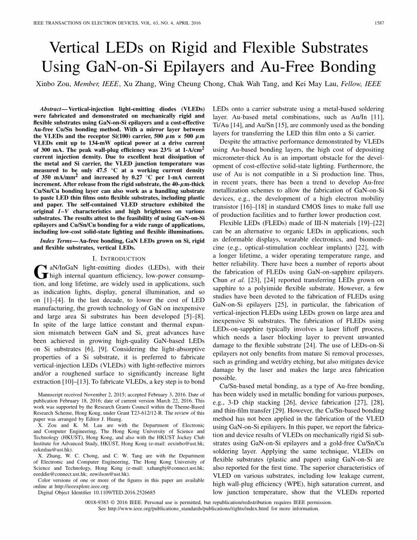
Fig. 1. (a) GaN LEDs grown on a 6-in Si substrate. (b) Cross-sectional image showing LED growth substrate bonded with a Si(100) carrierusing a Cu/Sn/Cu metal bonding layer.
here have great potential in fabricating low-cost yet high-performance lighting fixtures for various applications.
II. MATERIAL AND FABRICATION DETAILS
The GaN LEDs used in this paper were grown ona 6-in Si(111) substrate by AIXTRON Flip Top 1 × 6-inclosed couple showerhead metal organic chemical vapor depo-sition (MOCVD) reactor, equipped with LayTec’s EpiCurve-TT in situ monitor. The epilayers included a 1.2-μm-thickgraded AlGaN buffer, a 500-nm-thick undoped GaN layer,a 2-μm-thick Si-doped n-type GaN layer, ten pairs ofInGaN/GaN multiple quantum wells, and a 120-nm Mg-dopedp-type GaN [Fig. 1(a)].
The process steps of VLEDs on a Si(100) carrier are brieflydescribed as follows: a square mesa of LEDs was isolatedby etching GaN epilayers in trenches down to the Si(111)growth substrate. Then, the sidewalls of the LED mesaswere passivated by depositing a layer of SiO2 using plasma-enhanced chemical vapor deposition. Next, a layer of Indiumtin oxide (ITO) was deposited by an e-beam evaporator andannealed to form transparent ohmic contact with p-GaN. Sub-sequently, a layer of Al-based metal layer was deposited on topof ITO as a mirror layer and a seed layer, on which selectiveelectroplating of Cu and Sn was carried out on individualLED mesas. Then, the wafer was flipped upside down andbonded to a Si(100) carrier which has been preelectroplatedwith Cu and Sn. The thermocompression bonding process wasconducted by heating the samples to 280 °C and applyinga pressure of 15 N/cm2. After metal bonding, the original
Si(111) growth substrate was grinded down to 150-μm thickand eventually eliminated by inductively coupled plasma (ICP)etching using SF6-based gas. After further removal of theAlN/AlGaN buffer layer by dry etching, the n-GaN layer wasexposed and roughened by dipping the sample into 60 °C6-M KOH for 2 min. The whole process was finished bydepositing a layer of Ti/Al-based metal as n-electrode. Forthe fabrication of VLEDs on flexible substrates, the Si(100)carrier was replaced by a SiO2/Si(100) carrier, in which theSiO2 layer acts as a sacrificial layer for lifting VLEDs-on-metal off the rigid Si(100) substrate. Then, the VLEDs on themetal foil could be pasted onto flexible substrates, such asplastic and paper substrates through an adhesive layer.
III. RESULTS AND DISCUSSION
After MOCVD growth, the epitaxy quality and the surfacemorphology of the LED-on-Si(111) epitaxial structure wereexamined by high-resolution X-ray diffraction (XRD) andatomic force microscopy, respectively. The full-width at half-maximum of the XRD rocking curves were 440 and 553 arcsecfor (002) and (102) orientations, respectively, showing a goodcrystalline quality for optoelectronic devices. The LED alsoshowed a very smooth surface with a root mean squareroughness of only 1.4 nm for a 10 × 10 μm2 scan area.
A. VLEDs on Rigid Si(100) Carrier
Fig. 1(b) shows a cross-sectional image of a Cu/Sn/Cubonding layer, through which an LED sample grown onSi(111) was bonded onto a Si(100) carrier. The total bondingmetal thickness is ∼40 μm, which could be obtained within1 h by electroplating simultaneously on both the LED surfaceand the Si carrier surface. At a current density of 20 mA/cm2,the electroplating rate of Cu and Sn is 20 and 48 μm/h,respectively, which is much faster than the deposition rateof an e-beam evaporator. As shown in Fig. 1(b), no voidswere observed for the bonding interface, which provided firmsupport for the LED thin-film process and LED operations.
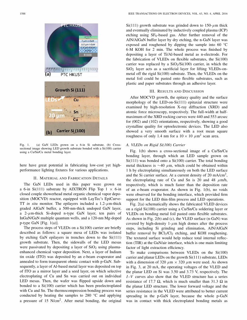
Fig. 2(a) schematically shows the fabricated VLED deviceson a rigid Si(100) carrier using a Cu/Sn/Cu soldering layer orVLEDs on bonding metal foil pasted onto flexible substrates.As shown in Fig. 2(b) and (c), the VLED surface (n-GaN) wascovered by high-density 1-μm high domes after the processsteps, including Si grinding and elimination, AlN/AlGaNbuffer removal by BCl3/Cl2 etching, and KOH roughening.The textured surface would help reduce total internal reflec-tion (TIR) at the GaN/air interface, which is one main limitingfactor of light extraction efficiency.
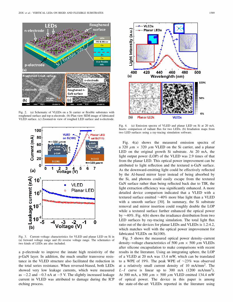
To make comparisons between VLEDs on the Si(100)carrier and planar LEDs on the growth Si(111) substrate, LEDswith a dimension of 320 μm × 320 μm were used. As shownin Fig. 3, at 20 mA, the operating voltages of the VLED andthe planar LED on Si was 3.50 and 3.73 V, respectively. TheI–V curves also show that the VLED structure has a seriesresistance of 17.7 �, which is much smaller than 31.3 � inthe planar LED structure. The lower forward voltage and theseries resistance in the VLED were attributed to better currentspreading in the p-GaN layer, because the whole p-GaNwas in contact with thick electroplated bonding metals as
ZOU et al.: VERTICAL LEDs ON RIGID AND FLEXIBLE SUBSTRATES 1589
Fig. 2. (a) Schematic of VLEDs on a Si carrier or flexible substrates withroughened surface and top n-electrode. (b) Plan view SEM image of fabricatedVLED surface. (c) Zoomed-in view of roughed LED surface and n-electrode.
Fig. 3. Current–voltage characteristics for VLED and planar LED on Si in(a) forward voltage range and (b) reverse voltage range. The schematics oftwo kinds of LEDs are also included.
a p-electrode to improve the innate high resistivity of thep-GaN layer. In addition, the much smaller transverse resis-tance in the VLED structure also facilitated the reduction inthe total series resistance. When reversed-biased, both LEDsshowed very low leakage currents, which were measuredas −2.2 and −0.3 nA at −5 V. The slightly increased leakagecurrent in VLED was attributed to damage during the ICPetching process.
Fig. 4. (a) Emission spectra of VLED and planar LED on Si at 20 mA.Insets: comparison of radiant flux for two LEDs. (b) Irradiation maps fromtwo LED surfaces using a ray-tracing simulation software.
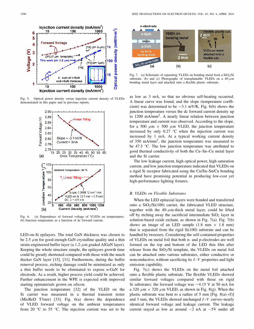
Fig. 4(a) shows the measured emission spectra ofa 320 μm × 320 μm VLED on the Si carrier, and a planarLED on the original growth Si substrate. At 20 mA, thelight output power (LOP) of the VLED was 2.9 times of thatfrom the planar LED. This optical power improvement can beattributed to light reflection and the textured n-GaN surface.As the downward-emitting light could be effectively reflectedby the Al-based mirror layer instead of being absorbed bythe Si, and photons could easily escape from the texturedGaN surface rather than being reflected back due to TIR, thelight extraction efficiency was significantly enhanced. A moredetailed device comparison indicated that a VLED with atextured surface emitted ∼40% more blue light than a VLEDwith a smooth surface [30]. In summary, the Si substrateremoval and mirror insertion could roughly double the LOPwhile a textured surface further enhanced the optical powerby ∼40%. Fig. 4(b) shows the irradiance distribution from twoLED surfaces by ray-tracing simulation. The total light fluxratio out of the devices for planar LEDs and VLEDs is 1.2:4.2,which matches well with the optical power improvement forfabricated VLEDs on Si(100).
Fig. 5 shows the measured optical power density–currentdensity–voltage characteristics of 500 μm × 500 μm VLEDsafter silicone encapsulation to make comparisons with recentresults in the literature. Using an integrating sphere, the LOPof a VLED at 20 mA was 13.4 mW, which can be translatedto a WPE of 19%. The peak WPE of ∼23% was observedat a relatively small current density of 10 mA/mm2. TheL–I curve is linear up to 300 mA (1200 mA/mm2).At 300 mA, a 500 μm × 500 μm VLED emitted 134.4 mWof optical power. The device in this paper is amongthe state-of-the-art VLEDs reported in the literature using
1590 IEEE TRANSACTIONS ON ELECTRON DEVICES, VOL. 63, NO. 4, APRIL 2016
Fig. 5. Optical power density versus injection current density of VLEDsdemonstrated in this paper and in previous reports.
Fig. 6. (a) Dependence of forward voltage of VLEDs on temperatures.(b) Junction temperature as a function of dc forward current.
LED-on-Si epilayers. The total GaN thickness was chosen tobe 2.5 μm for good enough GaN crystalline quality and a thinstrain-engineered buffer layer (a 1.2-μm graded AlGaN layer).Keeping the whole structure simple, the epilayers growth timecould be greatly shortened compared with those with the muchthicker GaN layer [15], [31]. Furthermore, during the bufferremoval process, etching damage could be minimized as onlya thin buffer needs to be eliminated to expose n-GaN forelectrode. As a result, higher process yield could be achieved.Further enhancement in the WPE is expected with improvedstarting epimaterials grown on silicon.
The junction temperature [32] of the VLED on theSi carrier was measured in a thermal transient tester(MicReD T3ster) [33]. Fig. 6(a) shows the dependenceof VLED forward voltage on the ambient temperaturesfrom 20 °C to 55 °C. The injection current was set to be
Fig. 7. (a) Schematic of separating VLEDs on bonding metal from a SiO2/Sisubstrate. (b) and (c) Photographs of transplantable VLEDs on a 40-μmbonding metal layer and attached onto a flexible plastic substrate.
as low as 3 mA, so that no obvious self-heating occurred.A linear curve was found, and the slope (temperature coeffi-cient) was determined to be −3.1 mV/K. Fig. 6(b) shows thejunction temperature versus the dc forward current density upto 1200 mA/mm2. A nearly linear relation between junctiontemperature and current was observed. According to the slope,for a 500 μm × 500 μm VLED, the junction temperatureincreased by only 0.27 °C when the injection current wasincreased by 1 mA. At a typical working current densityof 350 mA/mm2, the junction temperature was measured tobe 47.5 °C. The low junction temperature was attributed togood thermal conductivity of both the Cu–Sn–Cu metal layerand the Si carrier.
The low leakage current, high optical power, high saturationcurrent, and low junction temperature indicated that VLEDs ona rigid Si receptor fabricated using the Cu/Sn–Sn/Cu bondingmethod have promising potential in producing low-cost yethigh-performance lighting fixtures.
B. VLEDs on Flexible Substrates
When the LED epitaxial layers were bonded and transferredonto a SiO2/Si(100) carrier, the fabricated VLED structure,together with the 40-μm-thick metal layer, could be liftedoff by etching away the sacrificial intermediate SiO2 layer insolution-based oxide etchant, as shown in Fig. 7(a). Fig. 7(b)shows an image of an LED sample (1.8 mm × 1.8 mm)that is separated from the rigid Si(100) substrate and can behandled by tweezers. Considering the self-contained propertiesof VLEDs on metal foil that both n- and p-electrodes are wellformed on the top and bottom of the LED thin film afterrelease from the SiO2/Si template, the VLEDs on metal foilcan be attached onto various substrates, either conductive ornonconductive, without sacrificing its I–V properties and lightemission capability.
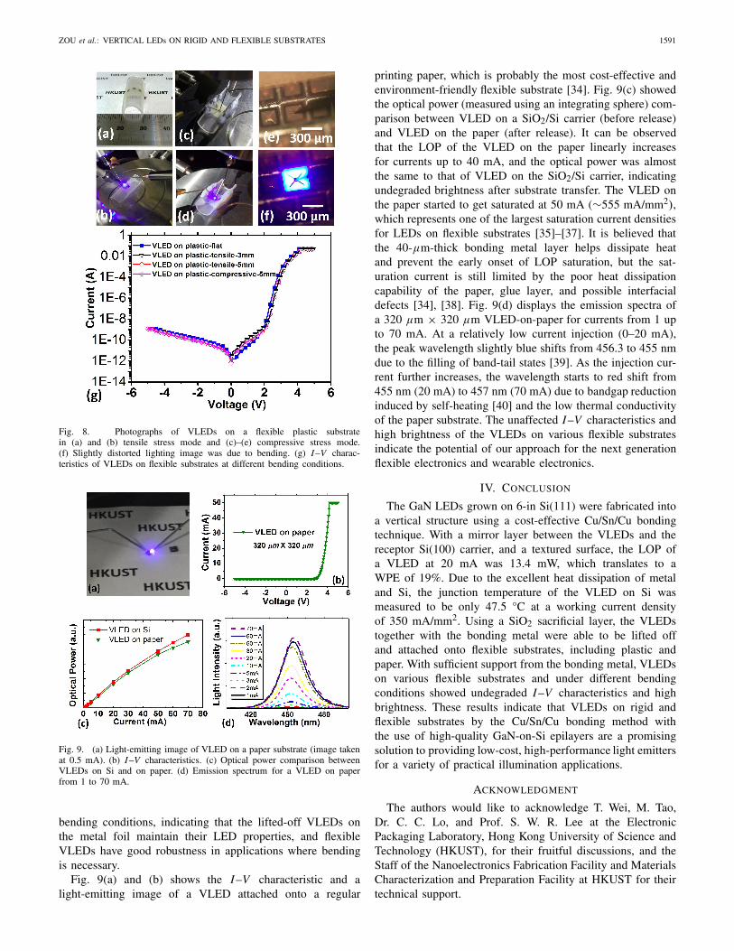
Fig. 7(c) shows the VLEDs on the metal foil attachedonto a flexible plastic substrate. The flexible VLEDs showedsimilar forward voltages compared with those on rigidSi substrates: the forward voltage was ∼4.15 V at 50 mA fora 320 μm × 320 μm VLED, as shown in Fig. 8(g). When theplastic substrate was bent to a radius of 5 mm [Fig. 8(a)–(f)]and 3 mm, the VLEDs showed unchanged I–V curves–nearlyidentical forward voltage and leakage current. The leakagecurrent stayed as low as around −2 nA at −5V under all
ZOU et al.: VERTICAL LEDs ON RIGID AND FLEXIBLE SUBSTRATES 1591
Fig. 8. Photographs of VLEDs on a flexible plastic substratein (a) and (b) tensile stress mode and (c)–(e) compressive stress mode.(f) Slightly distorted lighting image was due to bending. (g) I–V charac-teristics of VLEDs on flexible substrates at different bending conditions.
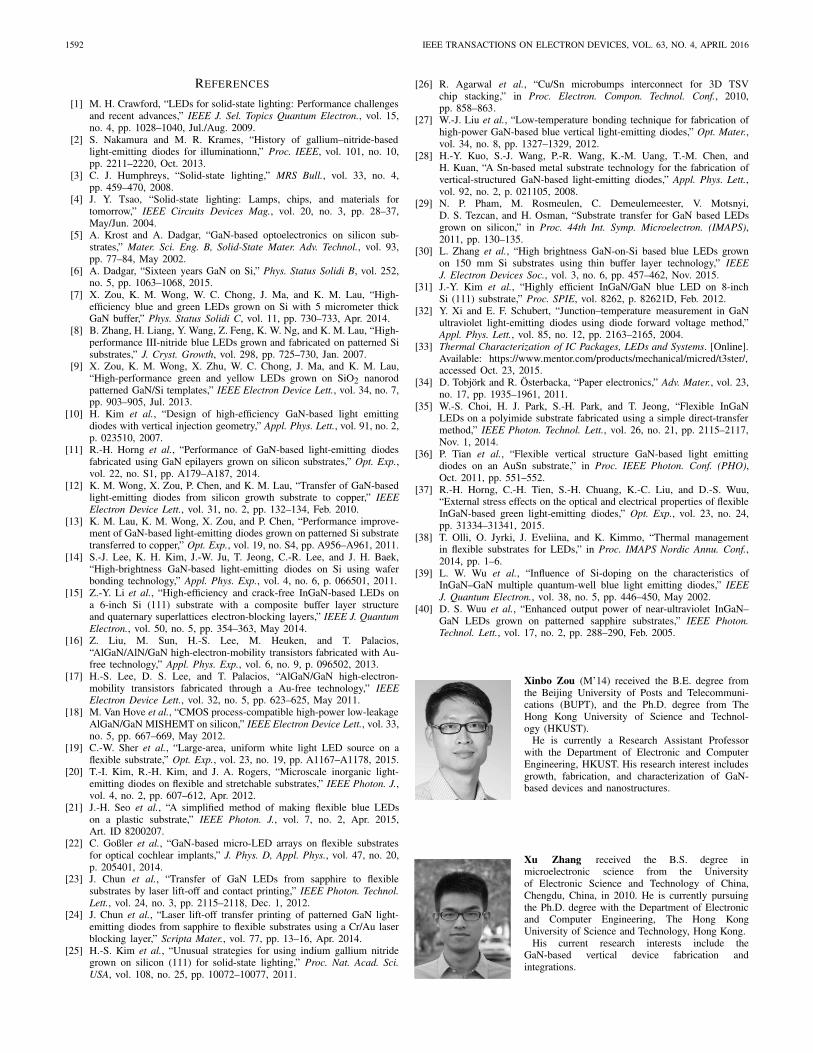
Fig. 9. (a) Light-emitting image of VLED on a paper substrate (image takenat 0.5 mA). (b) I–V characteristics. (c) Optical power comparison betweenVLEDs on Si and on paper. (d) Emission spectrum for a VLED on paperfrom 1 to 70 mA.
bending conditions, indicating that the lifted-off VLEDs onthe metal foil maintain their LED properties, and flexibleVLEDs have good robustness in applications where bendingis necessary.
Fig. 9(a) and (b) shows the I–V characteristic and alight-emitting image of a VLED attached onto a regular
printing paper, which is probably the most cost-effective andenvironment-friendly flexible substrate [34]. Fig. 9(c) showedthe optical power (measured using an integrating sphere) com-parison between VLED on a SiO2/Si carrier (before release)and VLED on the paper (after release). It can be observedthat the LOP of the VLED on the paper linearly increasesfor currents up to 40 mA, and the optical power was almostthe same to that of VLED on the SiO2/Si carrier, indicatingundegraded brightness after substrate transfer. The VLED onthe paper started to get saturated at 50 mA (∼555 mA/mm2),which represents one of the largest saturation current densitiesfor LEDs on flexible substrates [35]–[37]. It is believed thatthe 40-μm-thick bonding metal layer helps dissipate heatand prevent the early onset of LOP saturation, but the sat-uration current is still limited by the poor heat dissipationcapability of the paper, glue layer, and possible interfacialdefects [34], [38]. Fig. 9(d) displays the emission spectra ofa 320 μm × 320 μm VLED-on-paper for currents from 1 upto 70 mA. At a relatively low current injection (0–20 mA),the peak wavelength slightly blue shifts from 456.3 to 455 nmdue to the filling of band-tail states [39]. As the injection cur-rent further increases, the wavelength starts to red shift from455 nm (20 mA) to 457 nm (70 mA) due to bandgap reductioninduced by self-heating [40] and the low thermal conductivityof the paper substrate. The unaffected I–V characteristics andhigh brightness of the VLEDs on various flexible substratesindicate the potential of our approach for the next generationflexible electronics and wearable electronics.
IV. CONCLUSION
The GaN LEDs grown on 6-in Si(111) were fabricated intoa vertical structure using a cost-effective Cu/Sn/Cu bondingtechnique. With a mirror layer between the VLEDs and thereceptor Si(100) carrier, and a textured surface, the LOP ofa VLED at 20 mA was 13.4 mW, which translates to aWPE of 19%. Due to the excellent heat dissipation of metaland Si, the junction temperature of the VLED on Si wasmeasured to be only 47.5 °C at a working current densityof 350 mA/mm2. Using a SiO2 sacrificial layer, the VLEDstogether with the bonding metal were able to be lifted offand attached onto flexible substrates, including plastic andpaper. With sufficient support from the bonding metal, VLEDson various flexible substrates and under different bendingconditions showed undegraded I–V characteristics and highbrightness. These results indicate that VLEDs on rigid andflexible substrates by the Cu/Sn/Cu bonding method withthe use of high-quality GaN-on-Si epilayers are a promisingsolution to providing low-cost, high-performance light emittersfor a variety of practical illumination applications.
ACKNOWLEDGMENT
The authors would like to acknowledge T. Wei, M. Tao,Dr. C. C. Lo, and Prof. S. W. R. Lee at the ElectronicPackaging Laboratory, Hong Kong University of Science andTechnology (HKUST), for their fruitful discussions, and theStaff of the Nanoelectronics Fabrication Facility and MaterialsCharacterization and Preparation Facility at HKUST for theirtechnical support.
1592 IEEE TRANSACTIONS ON ELECTRON DEVICES, VOL. 63, NO. 4, APRIL 2016
REFERENCES
[1] M. H. Crawford, “LEDs for solid-state lighting: Performance challengesand recent advances,” IEEE J. Sel. Topics Quantum Electron., vol. 15,no. 4, pp. 1028–1040, Jul./Aug. 2009.
[2] S. Nakamura and M. R. Krames, “History of gallium–nitride-basedlight-emitting diodes for illuminationn,” Proc. IEEE, vol. 101, no. 10,pp. 2211–2220, Oct. 2013.
[3] C. J. Humphreys, “Solid-state lighting,” MRS Bull., vol. 33, no. 4,pp. 459–470, 2008.
[4] J. Y. Tsao, “Solid-state lighting: Lamps, chips, and materials fortomorrow,” IEEE Circuits Devices Mag., vol. 20, no. 3, pp. 28–37,May/Jun. 2004.
[5] A. Krost and A. Dadgar, “GaN-based optoelectronics on silicon sub-strates,” Mater. Sci. Eng. B, Solid-State Mater. Adv. Technol., vol. 93,pp. 77–84, May 2002.
[6] A. Dadgar, “Sixteen years GaN on Si,” Phys. Status Solidi B, vol. 252,no. 5, pp. 1063–1068, 2015.
[7] X. Zou, K. M. Wong, W. C. Chong, J. Ma, and K. M. Lau, “High-efficiency blue and green LEDs grown on Si with 5 micrometer thickGaN buffer,” Phys. Status Solidi C, vol. 11, pp. 730–733, Apr. 2014.
[8] B. Zhang, H. Liang, Y. Wang, Z. Feng, K. W. Ng, and K. M. Lau, “High-performance III-nitride blue LEDs grown and fabricated on patterned Sisubstrates,” J. Cryst. Growth, vol. 298, pp. 725–730, Jan. 2007.
[9] X. Zou, K. M. Wong, X. Zhu, W. C. Chong, J. Ma, and K. M. Lau,“High-performance green and yellow LEDs grown on SiO2 nanorodpatterned GaN/Si templates,” IEEE Electron Device Lett., vol. 34, no. 7,pp. 903–905, Jul. 2013.
[10] H. Kim et al., “Design of high-efficiency GaN-based light emittingdiodes with vertical injection geometry,” Appl. Phys. Lett., vol. 91, no. 2,p. 023510, 2007.
[11] R.-H. Horng et al., “Performance of GaN-based light-emitting diodesfabricated using GaN epilayers grown on silicon substrates,” Opt. Exp.,vol. 22, no. S1, pp. A179–A187, 2014.
[12] K. M. Wong, X. Zou, P. Chen, and K. M. Lau, “Transfer of GaN-basedlight-emitting diodes from silicon growth substrate to copper,” IEEEElectron Device Lett., vol. 31, no. 2, pp. 132–134, Feb. 2010.
[13] K. M. Lau, K. M. Wong, X. Zou, and P. Chen, “Performance improve-ment of GaN-based light-emitting diodes grown on patterned Si substratetransferred to copper,” Opt. Exp., vol. 19, no. S4, pp. A956–A961, 2011.
[14] S.-J. Lee, K. H. Kim, J.-W. Ju, T. Jeong, C.-R. Lee, and J. H. Baek,“High-brightness GaN-based light-emitting diodes on Si using waferbonding technology,” Appl. Phys. Exp., vol. 4, no. 6, p. 066501, 2011.
[15] Z.-Y. Li et al., “High-efficiency and crack-free InGaN-based LEDs ona 6-inch Si (111) substrate with a composite buffer layer structureand quaternary superlattices electron-blocking layers,” IEEE J. QuantumElectron., vol. 50, no. 5, pp. 354–363, May 2014.
[16] Z. Liu, M. Sun, H.-S. Lee, M. Heuken, and T. Palacios,“AlGaN/AlN/GaN high-electron-mobility transistors fabricated with Au-free technology,” Appl. Phys. Exp., vol. 6, no. 9, p. 096502, 2013.
[17] H.-S. Lee, D. S. Lee, and T. Palacios, “AlGaN/GaN high-electron-mobility transistors fabricated through a Au-free technology,” IEEEElectron Device Lett., vol. 32, no. 5, pp. 623–625, May 2011.
[18] M. Van Hove et al., “CMOS process-compatible high-power low-leakageAlGaN/GaN MISHEMT on silicon,” IEEE Electron Device Lett., vol. 33,no. 5, pp. 667–669, May 2012.
[19] C.-W. Sher et al., “Large-area, uniform white light LED source on aflexible substrate,” Opt. Exp., vol. 23, no. 19, pp. A1167–A1178, 2015.
[20] T.-I. Kim, R.-H. Kim, and J. A. Rogers, “Microscale inorganic light-emitting diodes on flexible and stretchable substrates,” IEEE Photon. J.,vol. 4, no. 2, pp. 607–612, Apr. 2012.
[21] J.-H. Seo et al., “A simplified method of making flexible blue LEDson a plastic substrate,” IEEE Photon. J., vol. 7, no. 2, Apr. 2015,Art. ID 8200207.
[22] C. Goßler et al., “GaN-based micro-LED arrays on flexible substratesfor optical cochlear implants,” J. Phys. D, Appl. Phys., vol. 47, no. 20,p. 205401, 2014.
[23] J. Chun et al., “Transfer of GaN LEDs from sapphire to flexiblesubstrates by laser lift-off and contact printing,” IEEE Photon. Technol.Lett., vol. 24, no. 3, pp. 2115–2118, Dec. 1, 2012.
[24] J. Chun et al., “Laser lift-off transfer printing of patterned GaN light-emitting diodes from sapphire to flexible substrates using a Cr/Au laserblocking layer,” Scripta Mater., vol. 77, pp. 13–16, Apr. 2014.
[25] H.-S. Kim et al., “Unusual strategies for using indium gallium nitridegrown on silicon (111) for solid-state lighting,” Proc. Nat. Acad. Sci.USA, vol. 108, no. 25, pp. 10072–10077, 2011.
[26] R. Agarwal et al., “Cu/Sn microbumps interconnect for 3D TSVchip stacking,” in Proc. Electron. Compon. Technol. Conf., 2010,pp. 858–863.
[27] W.-J. Liu et al., “Low-temperature bonding technique for fabrication ofhigh-power GaN-based blue vertical light-emitting diodes,” Opt. Mater.,vol. 34, no. 8, pp. 1327–1329, 2012.
[28] H.-Y. Kuo, S.-J. Wang, P.-R. Wang, K.-M. Uang, T.-M. Chen, andH. Kuan, “A Sn-based metal substrate technology for the fabrication ofvertical-structured GaN-based light-emitting diodes,” Appl. Phys. Lett.,vol. 92, no. 2, p. 021105, 2008.
[29] N. P. Pham, M. Rosmeulen, C. Demeulemeester, V. Motsnyi,D. S. Tezcan, and H. Osman, “Substrate transfer for GaN based LEDsgrown on silicon,” in Proc. 44th Int. Symp. Microelectron. (IMAPS),2011, pp. 130–135.
[30] L. Zhang et al., “High brightness GaN-on-Si based blue LEDs grownon 150 mm Si substrates using thin buffer layer technology,” IEEEJ. Electron Devices Soc., vol. 3, no. 6, pp. 457–462, Nov. 2015.
[31] J.-Y. Kim et al., “Highly efficient InGaN/GaN blue LED on 8-inchSi (111) substrate,” Proc. SPIE, vol. 8262, p. 82621D, Feb. 2012.
[32] Y. Xi and E. F. Schubert, “Junction–temperature measurement in GaNultraviolet light-emitting diodes using diode forward voltage method,”Appl. Phys. Lett., vol. 85, no. 12, pp. 2163–2165, 2004.
[33] Thermal Characterization of IC Packages, LEDs and Systems. [Online].Available: https://www.mentor.com/products/mechanical/micred/t3ster/,accessed Oct. 23, 2015.
[34] D. Tobjörk and R. Österbacka, “Paper electronics,” Adv. Mater., vol. 23,no. 17, pp. 1935–1961, 2011.
[35] W.-S. Choi, H. J. Park, S.-H. Park, and T. Jeong, “Flexible InGaNLEDs on a polyimide substrate fabricated using a simple direct-transfermethod,” IEEE Photon. Technol. Lett., vol. 26, no. 21, pp. 2115–2117,Nov. 1, 2014.
[36] P. Tian et al., “Flexible vertical structure GaN-based light emittingdiodes on an AuSn substrate,” in Proc. IEEE Photon. Conf. (PHO),Oct. 2011, pp. 551–552.
[37] R.-H. Horng, C.-H. Tien, S.-H. Chuang, K.-C. Liu, and D.-S. Wuu,“External stress effects on the optical and electrical properties of flexibleInGaN-based green light-emitting diodes,” Opt. Exp., vol. 23, no. 24,pp. 31334–31341, 2015.
[38] T. Olli, O. Jyrki, J. Eveliina, and K. Kimmo, “Thermal managementin flexible substrates for LEDs,” in Proc. IMAPS Nordic Annu. Conf.,2014, pp. 1–6.
[39] L. W. Wu et al., “Influence of Si-doping on the characteristics ofInGaN–GaN multiple quantum-well blue light emitting diodes,” IEEEJ. Quantum Electron., vol. 38, no. 5, pp. 446–450, May 2002.
[40] D. S. Wuu et al., “Enhanced output power of near-ultraviolet InGaN–GaN LEDs grown on patterned sapphire substrates,” IEEE Photon.Technol. Lett., vol. 17, no. 2, pp. 288–290, Feb. 2005.
Xinbo Zou (M’14) received the B.E. degree fromthe Beijing University of Posts and Telecommuni-cations (BUPT), and the Ph.D. degree from TheHong Kong University of Science and Technol-ogy (HKUST).
He is currently a Research Assistant Professorwith the Department of Electronic and ComputerEngineering, HKUST. His research interest includesgrowth, fabrication, and characterization of GaN-based devices and nanostructures.
Xu Zhang received the B.S. degree inmicroelectronic science from the Universityof Electronic Science and Technology of China,Chengdu, China, in 2010. He is currently pursuingthe Ph.D. degree with the Department of Electronicand Computer Engineering, The Hong KongUniversity of Science and Technology, Hong Kong.
His current research interests include theGaN-based vertical device fabrication andintegrations.
ZOU et al.: VERTICAL LEDs ON RIGID AND FLEXIBLE SUBSTRATES 1593
Wing Cheung Chong received the bachelor’s(Hons.) and M.Phil. degrees in electronic andcomputer engineering from The Hong Kong Uni-versity of Science and Technology, Hong Kong,in 2005 and 2007, respectively, where he is currentlypursuing the Ph.D. degree with the Electronic andComputer Engineering Department.
His current research interests include cost-effective, high-brightness LED-processing techni-ques, and next-generation LED-based microdisplaytechnology.
Chak Wah Tang received the M.S. degree fromTaiwan National Cheng Kung University.
He is currently a Senior Technical Officer withthe Department of Electronic and Computer Engi-neering, The Hong Kong University of Science andTechnology. His current interests include epitaxialgrowth of III-V materials and their characterizations.
Kei May Lau (S’78–M’80–SM’92–F’01) receivedthe B.S. and M.S. degrees in physics from theUniversity of Minnesota, Minneapolis, and the Ph.D.degree in electrical engineering from Rice Univer-sity, Houston, TX.
She was a professor at the University of Massa-chusetts, Amherst. She is a Fang Professor of Engi-neering at The Hong Kong University of Science andTechnology, engaging in compound semiconductormaterials and device research for high-speed andphotonic applications.
Related Documents


![GaN-based light-emitting diodes with graphene/indium tin ... · green spectral regions [1,2]. For example, gallium nitride (GaN)-based blue and green light-emitting diodes (LEDs)](https://static.cupdf.com/doc/110x72/5f02215f7e708231d402b8ad/gan-based-light-emitting-diodes-with-grapheneindium-tin-green-spectral-regions.jpg)


