EE141 – Fall 2005 Lecture 3 CMOS Manufacturing CMOS Manufacturing Design Rules Design Rules EE141 2 Administrative Stuff The course web-page is up • http://bwrc.eecs.berkeley.edu/Classes/ee141 • http://inst.eecs.berkeley.edu/~ee141 Labs start next week • Everyone should have an EECS instructional account • http://www-inst.eecs.berkeley.edu/ ~inst/newusers.html Homework #1 is due this Thursday before class • Drop-off box 240 Cory Homework #2 will post on Thursday, Sep-8

Welcome message from author
This document is posted to help you gain knowledge. Please leave a comment to let me know what you think about it! Share it to your friends and learn new things together.
Transcript

1
EE141 – Fall 2005Lecture 3
CMOS ManufacturingCMOS ManufacturingDesign RulesDesign Rules
EE141 2
Administrative Stuff
The course web-page is up• http://bwrc.eecs.berkeley.edu/Classes/ee141• http://inst.eecs.berkeley.edu/~ee141
Labs start next week• Everyone should have an EECS instructional account• http://www-inst.eecs.berkeley.edu/
~inst/newusers.html
Homework #1 is due this Thursday before class• Drop-off box 240 Cory
Homework #2 will post on Thursday, Sep-8

2
EE141 3
TA Office Hours
TA office hours in 197 Cory• Lynn Wang, Tue 1:30-2:30pm• Ke Lu, Wed 2-3pm
Check the newsgroup for questions
Email Dejan and TAs: [email protected]
EE141 4
Last Lecture
Last lecture• Design metrics
Today’s lecture• CMOS manufacturing process• CMOS design rules

3
EE141 5
Review
Design MetricsDesign Metrics• Cost• Reliability• Speed• Power
EE141 6
Total Cost
Cost per IC
Variable cost
volumecost fixed ICper cost variable ICper cost +=
yield test finalpackaging ofcost test die ofcost die ofcost cost variable ++
=

4
EE141 7
Die Cost
Single die
Wafer
Going up to 12” (30cm)
yield die*per wafer dies waferofcost die ofcost =
From: http://www.amd.com
EE141 8
Defects
α−
α×
+=area dieareaunit per defects1yield die
α ≈ 3, complexity of mfg. process
defects per unit area = 0.5 to 1 /cm2
cost of die = f (die area)4
5
EE141 9
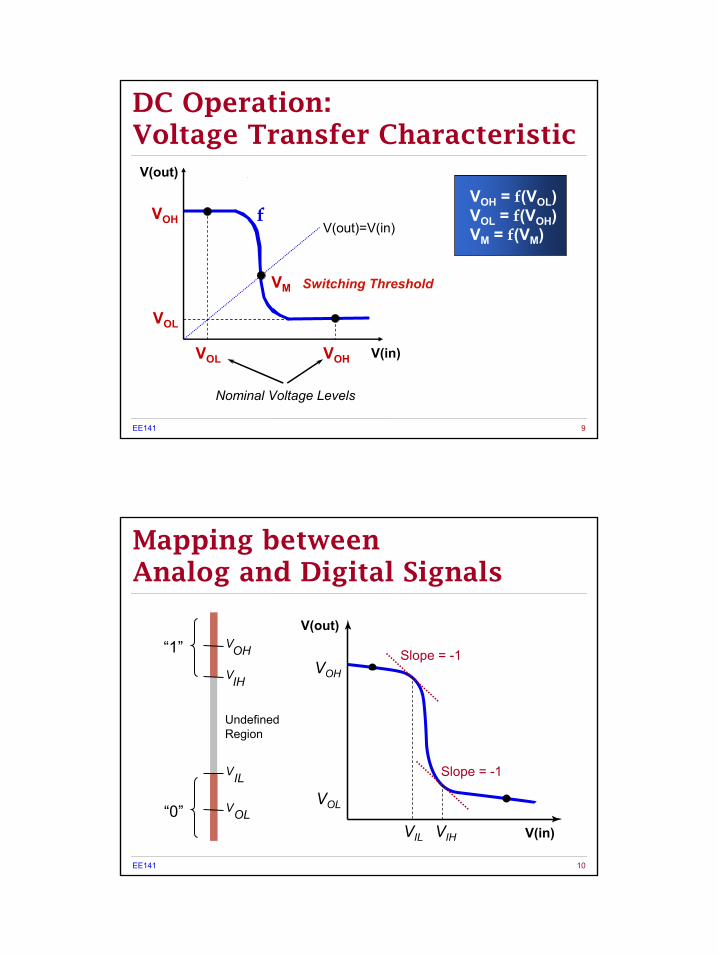
V(in)
V(out)
fV(out)=V(in)
Switching Threshold
Nominal Voltage Levels
VOH = f(VOL)VOL = f(VOH)VM = f(VM)
DC Operation:Voltage Transfer Characteristic
VOH
VOL
VM
VOL VOH
EE141 10
Slope = -1
Slope = -1
VOL
VIL
VIH
VOH
UndefinedRegion
Mapping between Analog and Digital Signals
“1”
“0”VOL
VOH
V(out)
V(in)VIL VIH

6
EE141 11
UndefinedRegion
Noise margin high:NMH = VOH – VIH
Noise margin low:NML = VIL – VOL
Gate Output
Gate Input
Definition of Noise Margins
NML
NMH
“0”
“1”
VOL
VOH
VIL
VIH
(Stage M) (Stage M+1)
EE141 12
Ri = ∞Ro = 0Fanout = ∞NMH = NML = VDD/2g = −∞
The Ideal Gate
V(in)
V(out)

7
EE141 13
Outline
Design MetricsDesign Metrics• Cost• Reliability• Speed• Power
EE141 14
Vout
tf
tpHL tpLH
trt
Vin
t
90%
10%
50%
50%2
pHLpLHp
ttt
+=
Performance: Delay Definitions

8
EE141 15
v0 v1 v5
v1 v2v0 v3 v4 v5
T = 2 × tp × N
Technology Characterization:Ring Oscillator for tp
EE141 16
Performance: FO4 Inverter
Measures quality of design across different technology generations
d

9
EE141 17
A First-Order RC Network
vout
v in C
R
Important model – matches delay of inverter
int
out vetv ⋅−= − )1()( τ
Step response:
RCt p 69.02ln =⋅= τPropagation delay:
EE141 18
Review
Design MetricsDesign Metrics• Cost• Reliability• Speed• Power
10
EE141 19
Power Dissipation
( )∫ ∫+ +
⋅=⋅=Tt
t
Tt
t supplydd
avg dttiT
VdttpT
P )(1
peakddpeak iVP ⋅=
( )tiVtitvtp supplydd ⋅=⋅= )()()(Instantaneous power
Peak power
Average power
EE141 20
Energy and Energy-Delay
Power-Delay Product (PDP) =
E = Energy per operation = Pavg × tp
Energy-Delay Product (EDP) =
quality metric of gate = E × tp

11
EE141 21
A First-Order RC Network
vout
vin CL
R
( )∫ ∫∫ ⋅=⋅=⋅=⋅=→
T V
ddLoutL
T
ddsupplydddd VCdVCVdttiVdttpE
0 0
2
010 )(
( ) ( )∫ ∫∫ ⋅⋅=⋅⋅=⋅⋅=⋅=T V
ddLoutoutL
T
capoutcapcapdd VCdVtVCdttitVdttpE
0 0
2
0 21)()(
1021
→= EEcap
EE141 22
Outline
MOS TransistorMOS Transistor
Manufacturing ProcessManufacturing Process
Design Rules & LayoutDesign Rules & Layout

12
EE141 23
The MOS Transistor
PolysiliconAluminum
EE141 24
CMOS Process

13
EE141 25
A Modern CMOS Process
p-well n-well
p+
p-epi
SiO2
AlCu
poly
n+
SiO2
p+
gate-oxide
Tungsten
TiSi2
DualDual--Well TrenchWell Trench--Isolated CMOS ProcessIsolated CMOS Process
EE141 26
Transistor Layout
p-well SiO2
poly
SiO2
n+
Cross-Sectional View
Layout View
poly
p-well

14
EE141 27
Circuit Under Design
VDDVDD
VinVout
M1
M2
M3
M4Vout2
EE141 28
Polysilicon
In Out
VDD
GND
PMOS 2λ
Metal 1
NMOS
OutIn
VDD
PMOS
NMOS
Contacts
N Well
CMOS Inverter

15
EE141 29
Two Inverters
Connect in Metal
VDD
Share power and ground
Abut cells
EE141 30
Outline
MOS TransistorMOS Transistor
Manufacturing ProcessManufacturing Process
Design Rules & LayoutDesign Rules & Layout

16
EE141 31
oxidation
opticalmask
processstep
photoresist coatingphotoresistremoval (ashing)
spin, rinse, dryacid etch
photoresist
stepper exposure
development
Typical operations in a single photolithographic cycle (from [Fullman]).
Photo-Lithographic Process
EE141 32
Patterning of SiO2
Si-substrate
Si-substrate Si-substrate
(a) Silicon base material
(b) After oxidation and depositionof negative photoresist
(c) Stepper exposure
PhotoresistSiO2
UV-lightPatternedoptical mask
Exposed resist
SiO2
Si-substrate
Si-substrate
Si-substrate
SiO2
SiO2
(d) After development and etching of resist,chemical or plasma etch of SiO2
(e) After etching
(f) Final result after removal of resist
Hardened resist
Hardened resist
Chemical or plasmaetch

17
EE141 33
CMOS Process at a Glance
Define active areasEtch and fill trenches
Implant well regions
Deposit and patternpolysilicon layer
Implant source and drainregions and substrate contacts
Create contact and via windowsDeposit and pattern metal layers
EE141 34
CMOS Process Walk-Through
p+
p-epi (a) Base material: p+ substrate with p-epi layer
p+
(c) After plasma etch of insulatingtrenches using the inverse of the active area mask
p+
p-epi SiO2
3SiN
4(b) After deposition of gate-oxide andsacrificial nitride (acts as abuffer layer)

18
EE141 35
CMOS Process Walk-Through
SiO2(d) After trench filling, CMPplanarization, and removal of sacrificial nitride
(e) After n-well and VTp adjust implants
n
(f) After p-well andVTn adjust implants
p
EE141 36
CMOS Process Walk-Through
(g) After polysilicon depositionand etch
poly(silicon)
(h) After n+ source/drain andp+source/drain implants. These
p+n+
steps also dope the polysilicon.
(i) After deposition of SiO2insulator and contact hole etch.
SiO2

19
EE141 37
CMOS Process Walk-Through
(j) After deposition and patterning of first Al layer.
Al
(k) After deposition of SiO 2insulator, etching of via’s,deposition and patterning ofsecond layer of Al.
AlSiO2
EE141 38
Advanced Metalization

20
EE141 39
Advanced Metalization
EE141 40
Outline
MOS TransistorMOS Transistor
Manufacturing ProcessManufacturing Process
Design Rules & LayoutDesign Rules & Layout

21
EE141 41
Design Rules
Interface between designer and process engineer
Guidelines for constructing process masks
Unit dimension: Minimum line width• Scalable design rules: lambda parameter• Absolute dimensions (micron rules)
EE141 42
Design Rules
Intra-layer• Widths, spacing
Inter-layer• Enclosures, overlaps
Special rules (sub-0.25µm)• Area, antenna rules, density rules

22
EE141 43
CMOS Process Layers
Layer
Polysilicon
Metal1
Metal2
Contact To Poly
Contact To Diffusion
Via
Well (p,n)
Active Area (n+,p+)
Color Representation
Yellow
Green
RedBlue
MagentaBlack
BlackBlack
Select (p+,n+) Green
EE141 44
Layers in 0.25µm CMOS Process

23
EE141 45
Design Rules
Intra-layer: widths, spacing
Inter-layer: enclosures, overlaps• Transistor rules• Contact and via rules• Well and substrate contacts
Special rules (sub-0.25µm)• Area, antenna rules, density rules
EE141 46
Intra-Layer Design Rules
Metal2 4
3
10
90
Well
Active3
3
Polysilicon2
2
Different PotentialSame Potential
Metal1 3
32
Contactor Via
Select2
or6
2Hole

24
EE141 47
1
2
5
3
Tran
sist
or
Inter Layer: Transistor Rules
Tran
sist
or
EE141 48
Inter Layer: Vias and Contacts
1
2
1
Via
Metal toPoly ContactMetal to
Active Contact
1
2
5
4
3 2
2

25
EE141 49
1
3 3
2
2
2
WellSubstrate
Select3
5
Inter Layer: Well and Substrate
EE141 50
Example: CMOS Inverter Layout
A A’
np-substrate Field
Oxidep+n+
In
Out
GND VDD
(a) Layout
(b) Cross-Section along A-A’
A A’

26
EE141 51
Layout Editor – MicroMagic
EE141 52
Layout Editor –Cadence Virtuoso
In1 In2Out
vdd
gnd

27
EE141 53
Design Rule Checker
poly_not_fet to all_diff minimum spacing = 0.14 um.
EE141 54
Sticks Diagram
1
3
In Out
VDD
GND
Stick diagram of inverter
• Dimensionless layout entities• Only topology is important
28
EE141 55
Next Lecture
MOS Transistor• Operation and modeling
Related Documents