EE141 1 gital Integrated Circuits 2nd Devices Lecture 6. CMOS Device Lecture 6. CMOS Device (cont) (cont) ECE 407/507

EE141 © Digital Integrated Circuits 2nd Devices 1 Lecture 6. CMOS Device (cont) ECE 407/507.
Dec 13, 2015
Welcome message from author
This document is posted to help you gain knowledge. Please leave a comment to let me know what you think about it! Share it to your friends and learn new things together.
Transcript
EE1411
© Digital Integrated Circuits2nd Devices
Lecture 6. CMOS Device (cont)Lecture 6. CMOS Device (cont)
ECE 407/507

EE1412
© Digital Integrated Circuits2nd Devices
NoticeNotice
Reading Assignment : chapter 1, chapter 3 (finish reading)
Both hw1 and lab1 are on the website hw1 due in one week (next Thurs.) Lab1 due in two week (the Thurs. after
next )
EE1413
© Digital Integrated Circuits2nd Devices

EE1414
© Digital Integrated Circuits2nd Devices
EE1415
© Digital Integrated Circuits2nd Devices
EE1416
© Digital Integrated Circuits2nd Devices
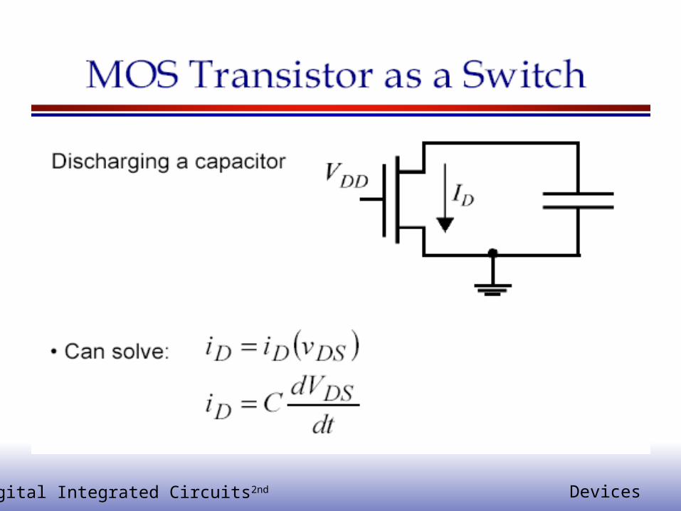
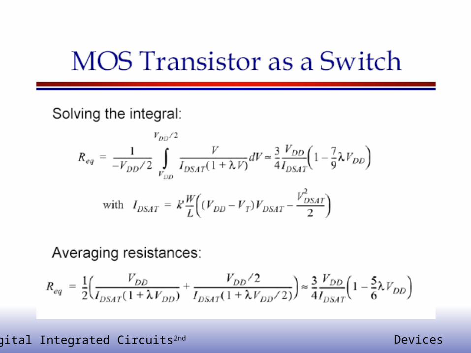
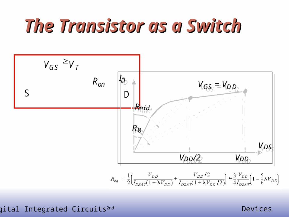
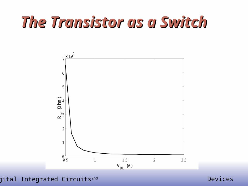
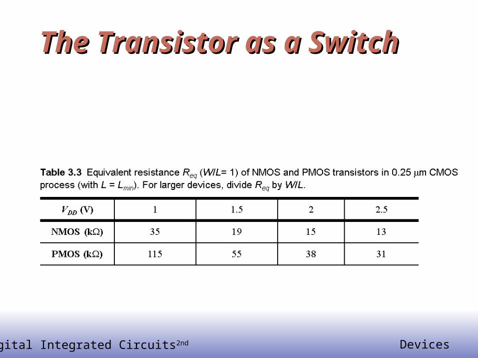
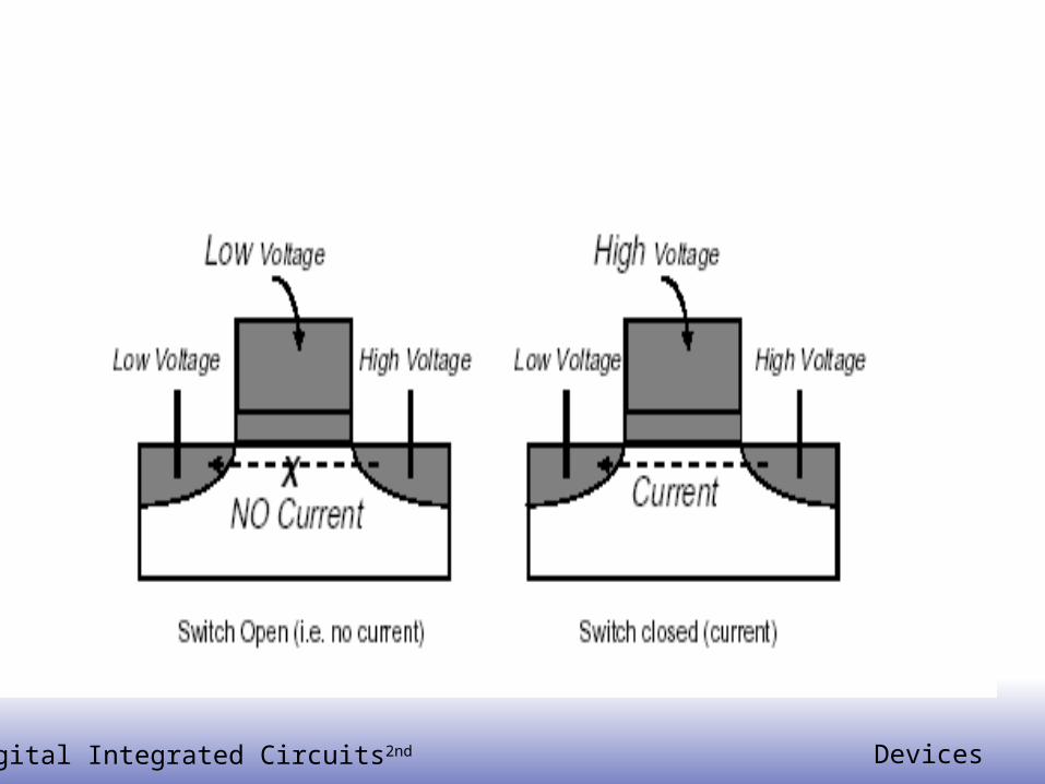
The Transistor as a SwitchThe Transistor as a Switch
VGS VT
RonS D
ID
VDS
VGS = VD D
VDD/2 VDD
R0
Rmid
ID
VDS
VGS = VD D
VDD/2 VDD
R0
Rmid
EE1417
© Digital Integrated Circuits2nd Devices
The Transistor as a SwitchThe Transistor as a Switch
0.5 1 1.5 2 2.50
1
2
3
4
5
6
7x 10
5
VDD
(V)
Req
(O
hm)
EE1418
© Digital Integrated Circuits2nd Devices
The Transistor as a SwitchThe Transistor as a Switch

EE1419
© Digital Integrated Circuits2nd Devices
EE14110
© Digital Integrated Circuits2nd Devices
EE14111
© Digital Integrated Circuits2nd Devices
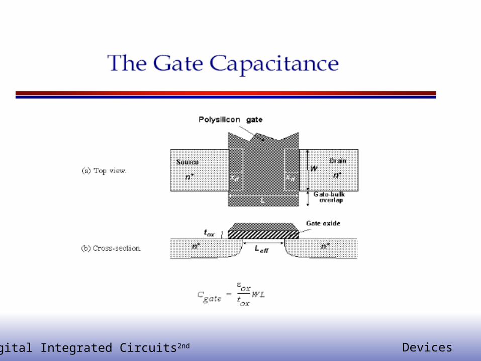
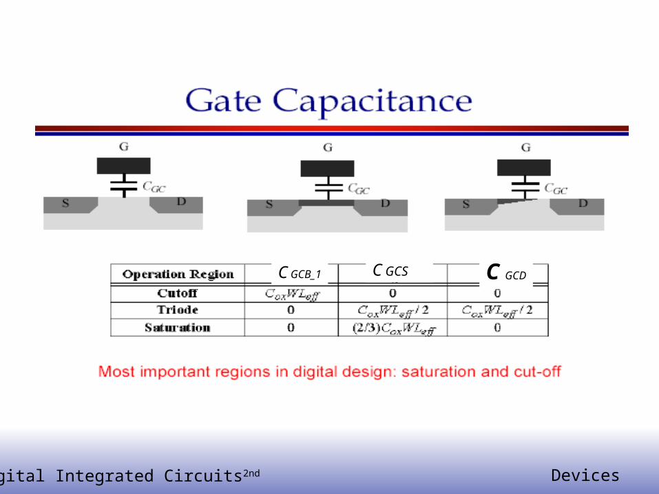
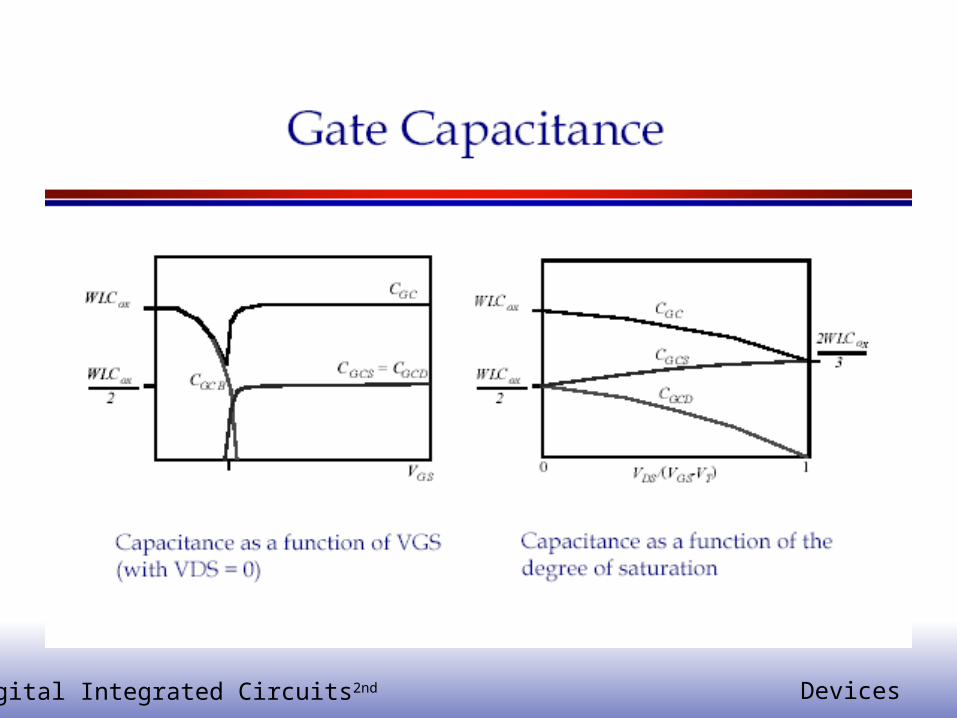
C GCB_1 C GCS C GCD
EE14112
© Digital Integrated Circuits2nd Devices
EE14113
© Digital Integrated Circuits2nd Devices

EE14114
© Digital Integrated Circuits2nd Devices

EE14115
© Digital Integrated Circuits2nd Devices
EE14116
© Digital Integrated Circuits2nd Devices
EE14117
© Digital Integrated Circuits2nd Devices

EE14118
© Digital Integrated Circuits2nd Devices
The Sub-Micron MOS TransistorThe Sub-Micron MOS Transistor
Threshold Variations Subthreshold Conduction Parasitic Resistances

EE14119
© Digital Integrated Circuits2nd Devices
Threshold VariationsThreshold Variations
VT
L
Long-channel threshold Low VDS threshold
Threshold as a function of the length (for low VDS)
Drain-induced barrier lowering (for low L)
VDS
VT

EE14120
© Digital Integrated Circuits2nd Devices
Sub-Threshold ConductionSub-Threshold Conduction
0 0.5 1 1.5 2 2.510
-12
10-10
10-8
10-6
10-4
10-2
VGS (V)
I D (
A)
VT
Linear
Exponential
Quadratic
Typical values for S:60 .. 100 mV/decade
The Slope Factor
ox
DnkT
qV
D C
CneII
GS
1 ,~ 0
S is VGS for ID2/ID1 =10
EE14121
© Digital Integrated Circuits2nd Devices
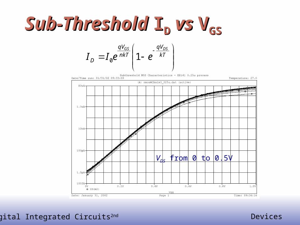
Sub-Threshold Sub-Threshold IIDD vs vs VVGSGS
VDS from 0 to 0.5V
kT
qV
nkT
qV
D
DSGS
eeII 10
EE14122
© Digital Integrated Circuits2nd Devices
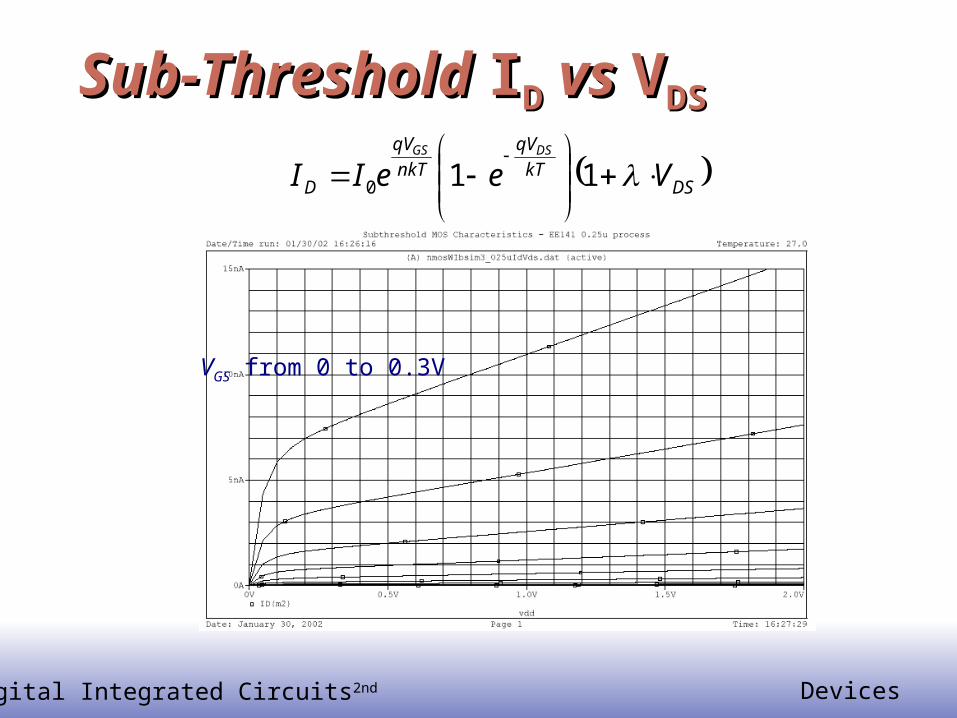
Sub-Threshold Sub-Threshold IIDD vs vs VVDSDS
DSkT
qV
nkT
qV
D VeeIIDSGS
110
VGS from 0 to 0.3V

EE14123
© Digital Integrated Circuits2nd Devices
Summary of MOSFET Operating Summary of MOSFET Operating RegionsRegions
Strong Inversion VGS > VT
Linear (Resistive) VDS < VDSAT
Saturated (Constant Current) VDS VDSAT
Weak Inversion (Sub-Threshold) VGS VT
Exponential in VGS with linear VDS dependence

EE14124
© Digital Integrated Circuits2nd Devices
Parasitic ResistancesParasitic Resistances
W
LD
Drain
Draincontact
Polysilicon gate
DS
G
RS RD
VGS,eff
EE14125
© Digital Integrated Circuits2nd Devices
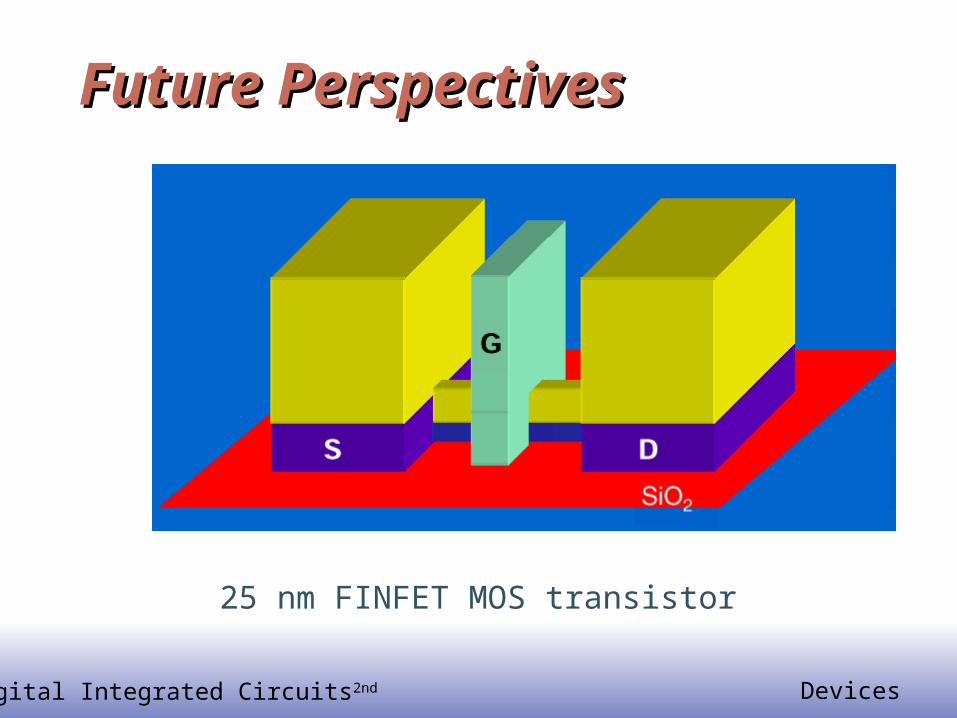
Future PerspectivesFuture Perspectives
25 nm FINFET MOS transistor

EE14126
© Digital Integrated Circuits2nd Devices
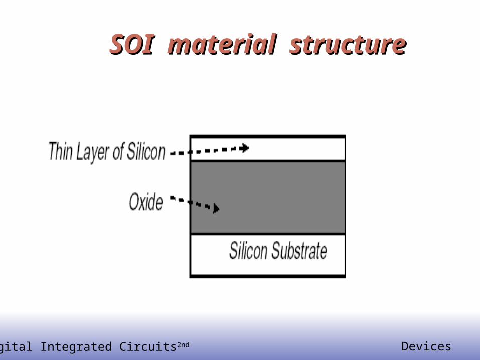
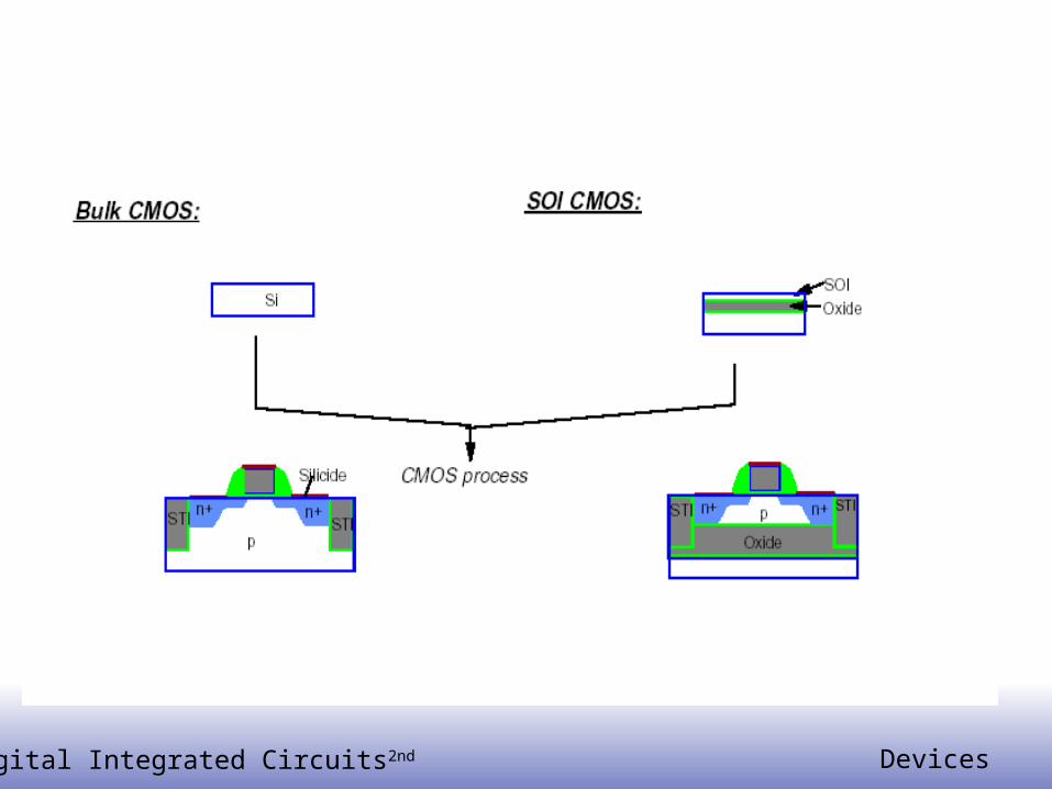
New Tech: Silicon On Insulator (SOI)New Tech: Silicon On Insulator (SOI)
Silicon wafers are highly perfect : critically important for achieving high device yield.
But a more radical change may be needed in the material structure, processing method, or device design in order to enhance the circuit performance.

EE14127
© Digital Integrated Circuits2nd Devices
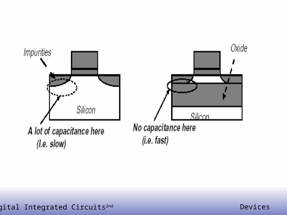
Why use SOIWhy use SOI
Extend the life of traditional silicon technology
Boost speed Reduce power consumption Solve some scaling difficulties

EE14128
© Digital Integrated Circuits2nd Devices
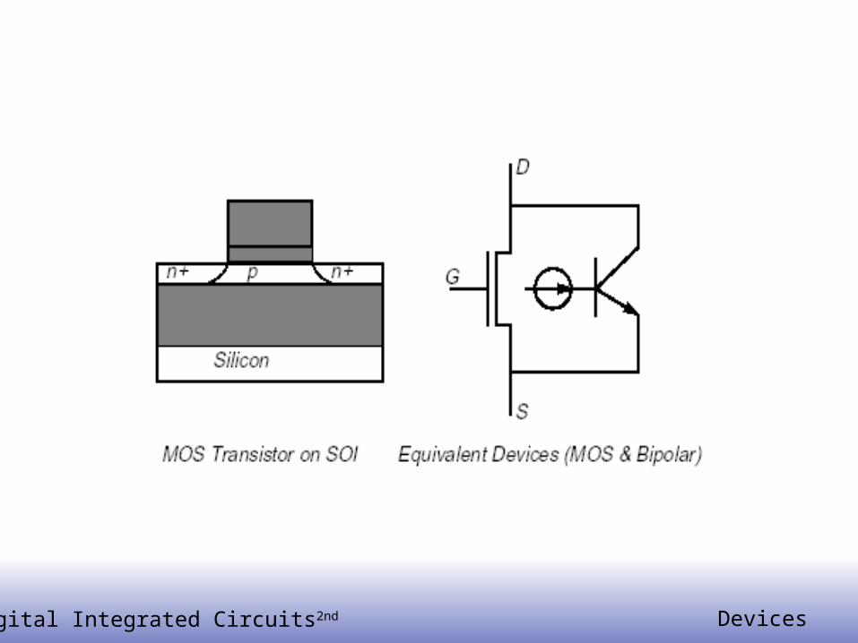
Transistor crosssectionTransistor crosssection
EE14129
© Digital Integrated Circuits2nd Devices
EE14130
© Digital Integrated Circuits2nd Devices
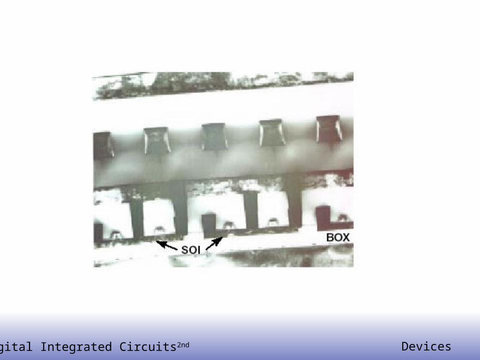
SOI material structure SOI material structure
EE14131
© Digital Integrated Circuits2nd Devices
EE14132
© Digital Integrated Circuits2nd Devices
EE14133
© Digital Integrated Circuits2nd Devices
EE14134
© Digital Integrated Circuits2nd Devices
EE14135
© Digital Integrated Circuits2nd Devices
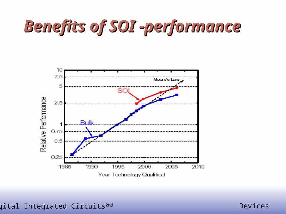
Benefits of SOI -performanceBenefits of SOI -performance

EE14136
© Digital Integrated Circuits2nd Devices
Benefits of SOI -- powerBenefits of SOI -- power
EE14137
© Digital Integrated Circuits2nd Devices
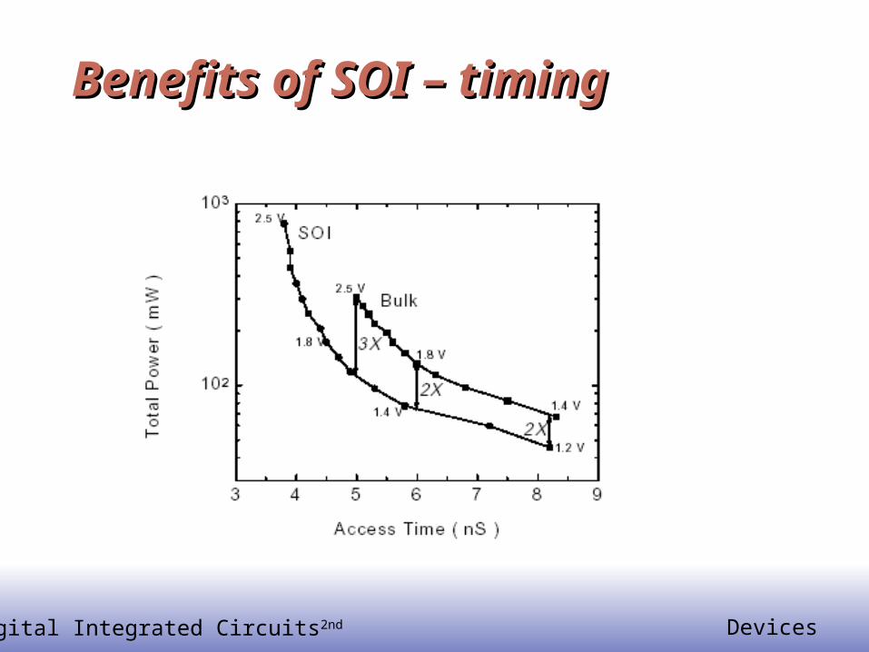
Benefits of SOI – timing Benefits of SOI – timing
EE14138
© Digital Integrated Circuits2nd Devices
SiGe: Silicon Germanium SiGe: Silicon Germanium
Used to be inefficient in chip production Extremely high frequencies: 60Ghz Very little power usage 70% faster, 35% less power
EE14139
© Digital Integrated Circuits2nd Devices
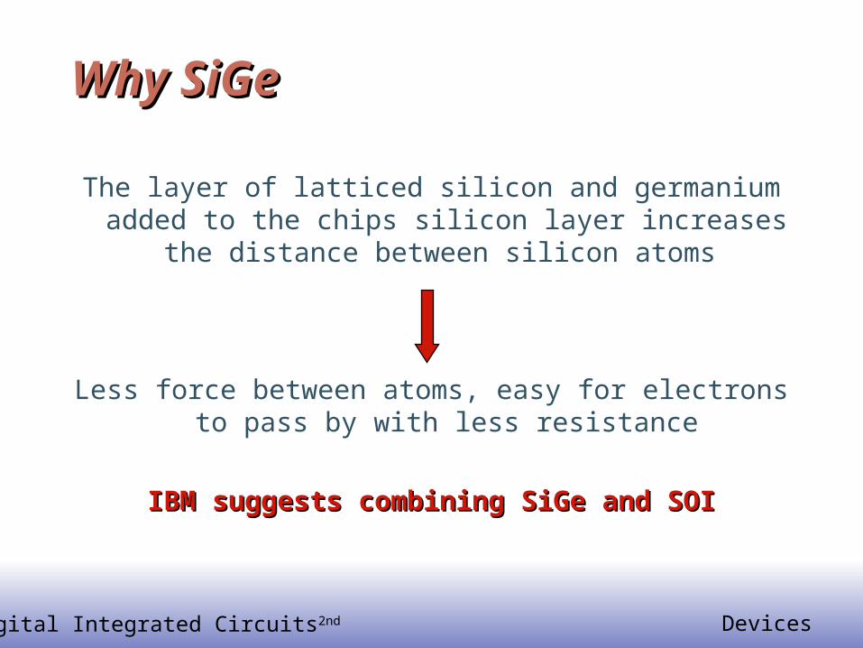
Why SiGeWhy SiGe
The layer of latticed silicon and germanium added to the chips silicon layer increases the distance between
silicon atoms
Less force between atoms, easy for electrons to pass by with less resistance
IBM suggests combining SiGe and SOIIBM suggests combining SiGe and SOI

EE14140
© Digital Integrated Circuits2nd Devices
Thermal problem with SiGeThermal problem with SiGe
The diagram above shows the effect of localized self-heating in the emitters(30C for 40mv)
Related Documents