EE141 1 EE141 1 EE141-S04 EE141 EE141- Spring 2004 Spring 2004 Digital Integrated Digital Integrated Circuits Circuits Lecture 20 Lecture 20 Power Power Sequential Logic Sequential Logic - Intro Intro EE141 2 EE141-S04 Administrative Stuff Administrative Stuff Midterm 2 Th 6:30pm in 277 Cory Material: – Wires – Complex logic – Arithmetic Review session on We at 5:30pm in 241 Cory Homework 7 posted – Due April 15

Welcome message from author
This document is posted to help you gain knowledge. Please leave a comment to let me know what you think about it! Share it to your friends and learn new things together.
Transcript

EE141
1
EE1411
EE141-S04
EE141EE141-- Spring 2004Spring 2004Digital Integrated Digital Integrated CircuitsCircuits
Lecture 20Lecture 20PowerPowerSequential Logic Sequential Logic -- IntroIntro
EE1412
EE141-S04
Administrative StuffAdministrative StuffMidterm 2 Th 6:30pm in 277 CoryMaterial:
– Wires– Complex logic– Arithmetic
Review session on We at 5:30pm in 241 CoryHomework 7 posted – Due April 15

EE141
2
EE1413
EE141-S04
Class MaterialClass Material
Last lectureMultipliers – Shifters – Power Intro
Today’s lecturePowerIntro to sequential logic
EE1414
EE141-S04
PowerPower

EE141
3
EE1415
EE141-S04
Power Dissipation in CMOSPower Dissipation in CMOS
Dynamic powerCharging capacitancesDominant today
Leakage powerLeaky transistorsConcern in low-activity, portable devices
Short circuit powerStatic power
E.g. pseudo-NMOS
EE1416
EE141-S04
Dynamic Power ConsumptionDynamic Power Consumption
( ) ( ) ∫∫ ∫ ====→
DDV
DDLoutLDD
T T
DDDDDD VCdvCVdttiVdttPE0
2
0 010
( ) ( ) ∫∫ ∫ ====DDV
DDLoutoutL
T T
LoutCC VCdvvCdttivdttPE0
2
0 021
Vdd
Vout
iL
CL
PMOS
NETWORK
NMOS
A1
AN
NETWORK
210 DDLVCE =→

EE141
4
EE1417
EE141-S04
Dynamic Power ConsumptionDynamic Power ConsumptionPower = Energy/transition • Transition rate
= CLVDD2 • f0→1
= CLVDD2 • f • P0→1
= CswitchedVDD2 • f
Power dissipation is data dependent – depends on the switching probabilitySwitched capacitance Cswitched = CL • P0→1
EE1418
EE141-S04
Transition Activity and PowerTransition Activity and PowerEnergy consumed in N cycles, EN:
EN = CL • VDD2 • n0→1
n0→1 – number of 0→1 transitions in N cycles
fVCN
nf
NE
P DDLN
N
Navg ⋅⋅⋅⎟⎠⎞
⎜⎝⎛=⋅= →
∞→∞→
210limlim
fN
nN
⋅= →
∞→→10
10 limα
fVCP DDLavg ⋅⋅⋅= →2
10α

EE141
5
EE1419
EE141-S04
“Dynamic” or timing dependent component
➟Type of Logic Function (NOR vs. XOR)“Static” component (does not account for timing)
➟Circuit Topology
➟Type of Logic Style (Static vs. Dynamic)
➟Signal Statistics
➟ Inter-signal Correlations
➟Signal Statistics and Correlations
Factors Affecting Transition ActivityFactors Affecting Transition Activity
EE14110
EE141-S04
Type of Logic Function: NOR vs. XORType of Logic Function: NOR vs. XOR
011
001
010
100OutBA
Example: Static 2-input NOR Gate
Assume signal probabilitiespA=1 = 1/2pB=1 = 1/2
Then transition probabilityp0→1 = pOut=0 x pOut=1
= 3/4 x 1/4 = 3/16
α0→1 = 3/16
If inputs switch every cycle
EE141
6
EE14111
EE141-S04
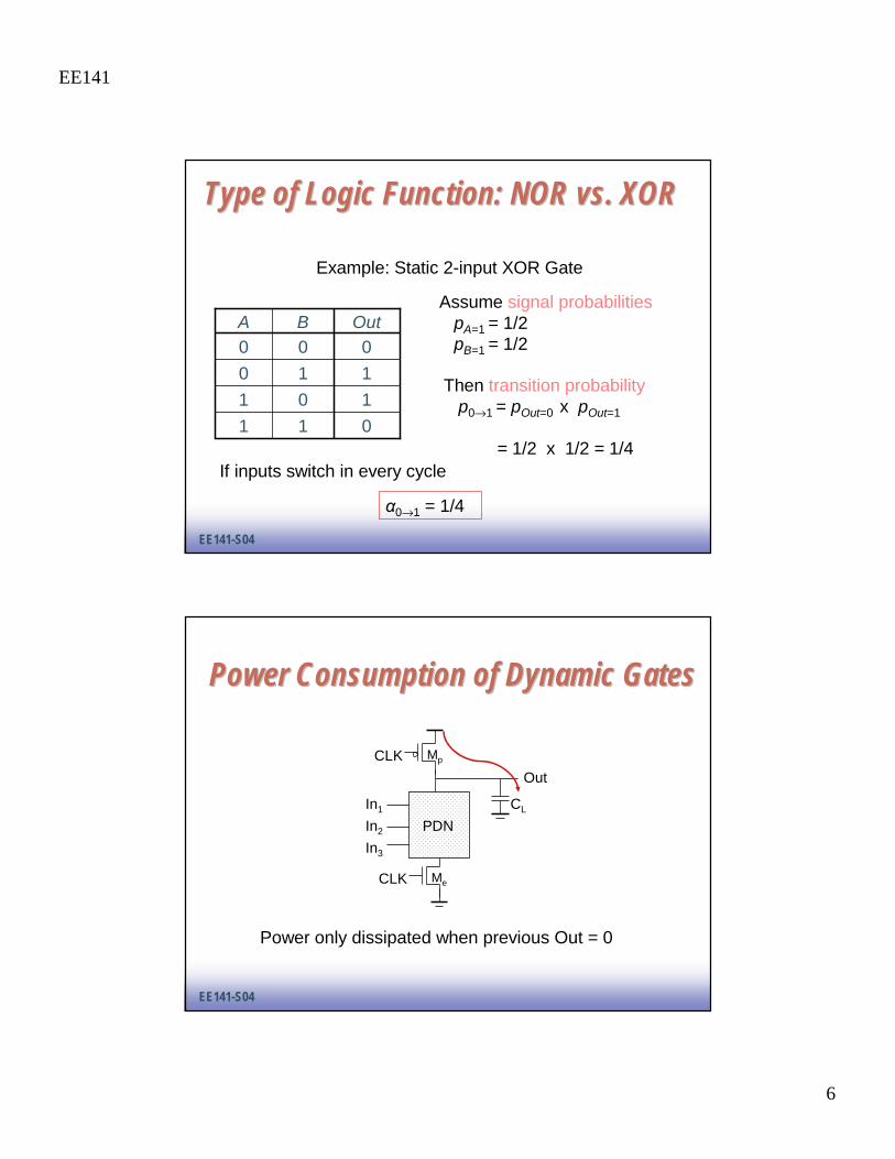
Type of Logic Function: NOR vs. XORType of Logic Function: NOR vs. XOR
011
101
110
000OutBA
Example: Static 2-input XOR Gate
Assume signal probabilitiespA=1 = 1/2pB=1 = 1/2
Then transition probabilityp0→1 = pOut=0 x pOut=1
= 1/2 x 1/2 = 1/4
α0→1 = 1/4
If inputs switch in every cycle
EE14112
EE141-S04
Power Consumption of Dynamic GatesPower Consumption of Dynamic Gates
In1
In2 PDN
In3
Me
Mp
CLK
CLK
Out
CL
Power only dissipated when previous Out = 0

EE141
7
EE14113
EE141-S04
Dynamic Power Consumption is Dynamic Power Consumption is Data DependentData Dependent
011
001
010
100OutBA
Dynamic 2-input NOR Gate
Assume signal probabilitiesPA=1 = 1/2PB=1 = 1/2
Then transition probabilityP0→1 = Pout=0 x Pout=1
= 3/4 x 1 = 3/4
Switching activity always higher in dynamic gates!P0→1 = Pout=0
EE14114
EE141-S04
Vdd
I
I
Vdd
IN
INB
OUTB OUT
Guaranteed transition for every operation!
α0->1 = 1
Dynamic CVSLDynamic CVSL

EE141
8
EE14115
EE141-S04
Problem: Problem: ReconvergentReconvergent FanoutFanout
A
B
X
Z
Reconvergence
P(Z = 1) = P(B = 1) . P(X = 1 | B=1)
Becomes complex and intractable fast
EE14116
EE141-S04
InterInter--Signal CorrelationsSignal Correlations
Logic withoutreconvergent fanout
Logic with reconvergent fanout
A
BZ
CA
Z
C
B
p0→1 = (1 – pApB) pApBP(Z = 1) = p(C=1 | B=1) p(B=1)
p0→1 = 0
Need to use conditional probabilities to model inter-signal correlationsCAD tools required for such analysis

EE141
9
EE14117
EE141-S04
GlitchingGlitching in Static CMOSin Static CMOSA
B
X
CZ
ABC 101 000
X
Z
Gate Delay
Also known asdynamic hazards
The result is correct,but there is extra power dissipated
EE14118
EE141-S04
Example: Chain of NOR GatesExample: Chain of NOR Gates1
Out1 Out2 Out3 Out4 Out5
0 200 400 6000.0
1.0
2.0
3.0
Time (ps)
Vol
tage
(V
)
Out8
Out6
Out2
Out6
Out1
Out3
Out7
Out5

EE141
10
EE14119
EE141-S04
Principles for Power ReductionPrinciples for Power Reduction
Prime choice: Reduce voltage!Recent years have seen an acceleration in supply voltage reductionDesign at very low voltages still open question (0.6 … 0.9 V by 2010!)Reducing thresholds to improve performance increases leakage
Reduce switching activityReduce physical capacitance
EE14120
EE141-S04
Sequential Logic

EE141
11
EE14121
EE141-S04
Sequential LogicSequential Logic
2 storage mechanisms
• positive feedback
• charge-based
COMBINATIONALLOGIC
Registers
Outputs
Next state
CLK
Q D
Current State
Inputs
EE14122
EE141-S04
Latch versus RegisterLatch versus Register
Latchstores data when clock is low
D
Clk
Q D
Clk
Q
Registerstores data when clock rises
Clk Clk
D D
Q Q
EE141
12
EE14123
EE141-S04
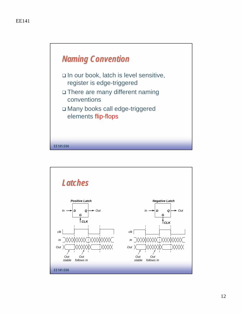
Naming ConventionNaming Convention
In our book, latch is level sensitive, register is edge-triggeredThere are many different naming conventionsMany books call edge-triggered elements flip-flops
EE14124
EE141-S04
LatchesLatches
In
clk
In
Out
Positive Latch
CLK
DG
Q
Out
Outstable
Outfollows In
In
clk
In
Out
Negative Latch
CLK
DG
Q
Out
Outstable
Outfollows In

EE141
13
EE14125
EE141-S04
NLatch
Logic
Logic
PLatch
φ
LatchLatch--Based DesignBased Design
• N latch is transparentwhen φ = 0
• P latch is transparent when φ = 1
EE14126
EE141-S04
Timing DefinitionsTiming Definitions
t
CLK
t
D
tc →q
tholdtsu
t
Q DATASTABLE
DATASTABLE
Register
CLK
D Q

EE141
14
EE14127
EE141-S04
Characterizing TimingCharacterizing Timing
Register Latch
Clk
D Q
tC →Q
Clk
D Q
tC →Q
tD →Q
EE14128
EE141-S04
Maximum Clock FrequencyMaximum Clock Frequency
FF
’s
LOGIC
tp,comb
φ
Also:tcdreg + tcdlogic > thold
tcd: contamination delay = minimum delay
tclk-Q + tp,comb + tsetup = T
EE141
15
EE14129
EE141-S04
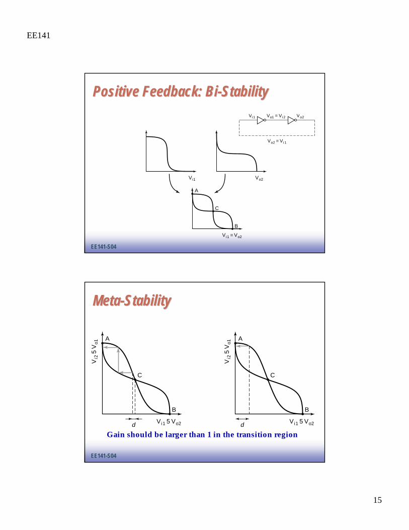
Positive Feedback: BiPositive Feedback: Bi--StabilityStabilityVi1 Vo2
Vo2 = Vi 1
Vo1 = Vi 2
V
o
1
Vi1
A
C
B
V
i
2
5
V
o
1
Vo2
V
i
2
5
V
o
1
Vi1 = Vo2
EE14130
EE141-S04
MetaMeta--StabilityStability
Gain should be larger than 1 in the transition region
A
C
d
B
Vi2
5V
o1
Vi1 5 Vo2
A
C
d
B
Vi2
5V
o1
Vi1 5 Vo2

EE141
16
EE14131
EE141-S04
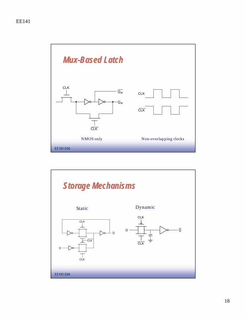
Writing into a Static LatchWriting into a Static Latch
CLK
CLK
CLK
D
Q D
CLK
CLK
D
Converting into a MUXForcing the state(can implement as NMOS-only)
Use the clock as a decoupling signal, that distinguishes between the transparent and opaque states
EE14132
EE141-S04
PseudoPseudo--Static LatchStatic Latch
D
CLK
CLK
D

EE141
17
EE14133
EE141-S04
MuxMux--Based LatchesBased LatchesNegative latch(transparent when CLK= 0)
Positive latch(transparent when CLK= 1)
CLK
1
0D
Q 0
CLK
1D
Q
InClkQClkQ ⋅+⋅= InClkQClkQ ⋅+⋅=
EE14134
EE141-S04
MuxMux--Based LatchBased Latch
CLK
CLK
CLK
D
Q
EE141
18
EE14135
EE141-S04
MuxMux--Based LatchBased Latch
CLK
CLK
CLK
CLK
QM
QM
NMOS only Non-overlapping clocks
EE14136
EE141-S04
Storage MechanismsStorage Mechanisms
D
CLK
CLK
Q
Dynamic
CLK
CLK
CLK
D
Q
Static

EE141
19
EE14137
EE141-S04
Next LectureNext Lecture
Sequential logic (cntd)
Related Documents