EE 330 Lecture 11 Back-end Processing Steps Devices in Semiconductor Processes • Resistors • Diodes

Welcome message from author
This document is posted to help you gain knowledge. Please leave a comment to let me know what you think about it! Share it to your friends and learn new things together.
Transcript

EE 330Lecture 11
Back-end Processing Steps
Devices in Semiconductor Processes• Resistors
• Diodes

Back-End Process Flow
Wafer Probe
Die Attach
Wafer Dicing
Wire Attach (bonding)
Package
Test
Ship
Review from Last Lecture
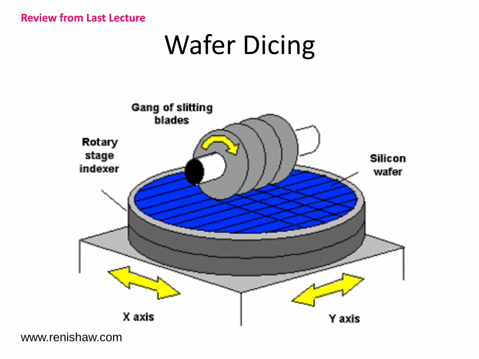
Wafer Dicing
www.renishaw.com
Review from Last Lecture
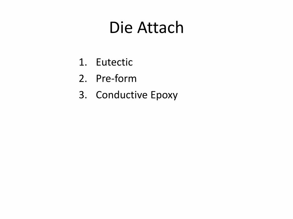
Die Attach
1. Eutectic
2. Pre-form
3. Conductive Epoxy
Electrical Connections (Bonding)
• Wire Bonding
• Bump Bonding
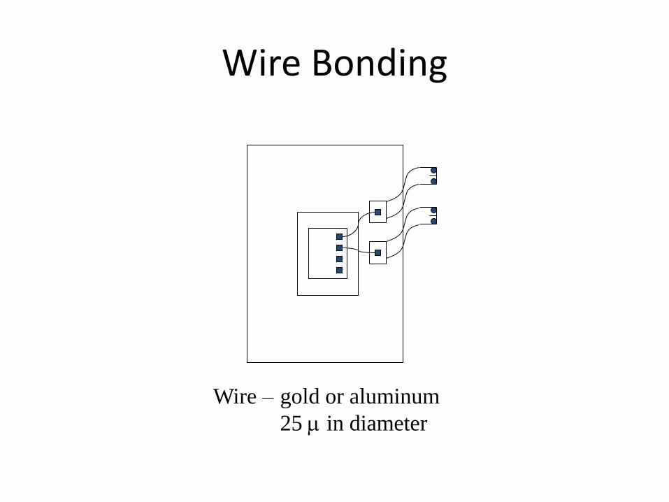
Wire Bonding
Wire – gold or aluminum
25 in diameter

Wire Bonding
Excellent Annimation showing process at :
http://www.kns.com/_Flash/CAP_BONDING_CYCLE.swf

Wire Bonding
www.kns.com
Ball Bond
Wedge Bond

Ball Bonding Steps
www.kns.com
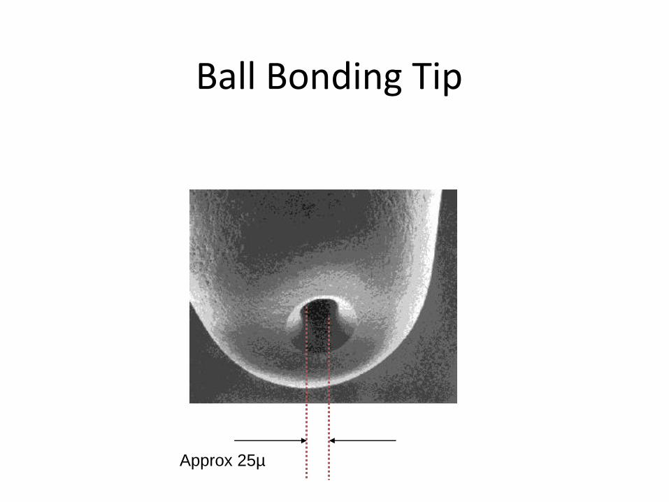
Ball Bonding Tip
Approx 25µ

Wire Bonding
Ball Bond Termination Bond
Ball Bond Photograph
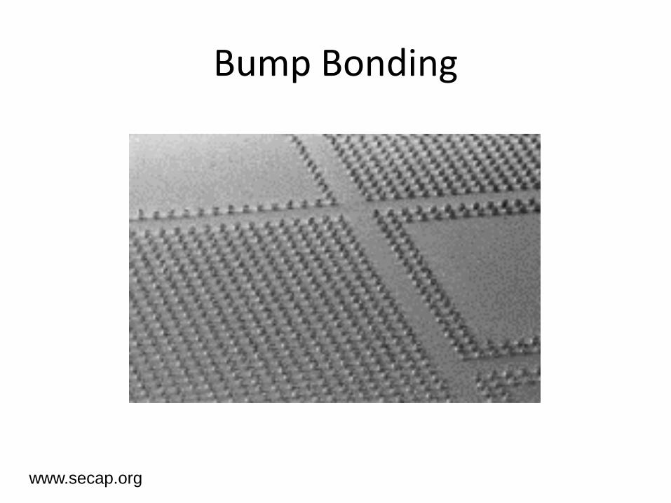
Bump Bonding
www.secap.org

Packaging
1. Many variants in packages now available
2. Considerable development ongoing on developing packaging technology
3. Cost can vary from few cents to tens of dollars
4. Must minimize product loss after packaged
5. Choice of package for a product is serious business
6. Designer invariably needs to know packaging plans and package models
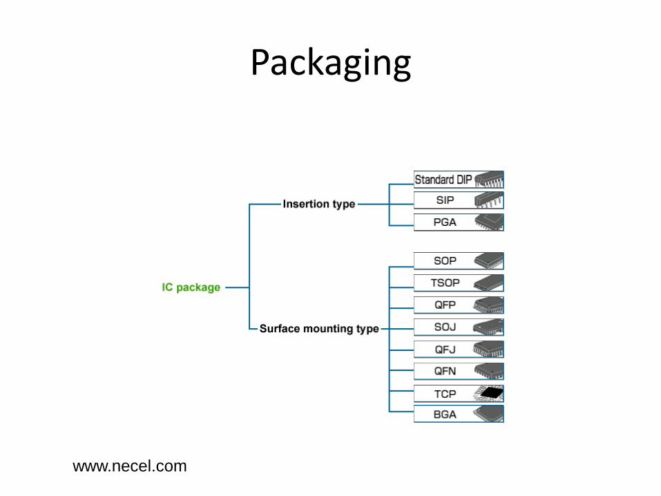
Packaging
www.necel.com

Packaging
www.necel.com

Pin Pitch Varies with Package Technology
From Wikipedia, Sept 20, 2010http://en.wikipedia.org/wiki/List_of_chip_carriers
http://www.electroiq.com/index/display/packaging-article-
display/234467/articles/advanced-packaging/volume-
14/issue-8/features/the-back-end-process/materials-and-
methods-for-ic-package-assemblies.htm
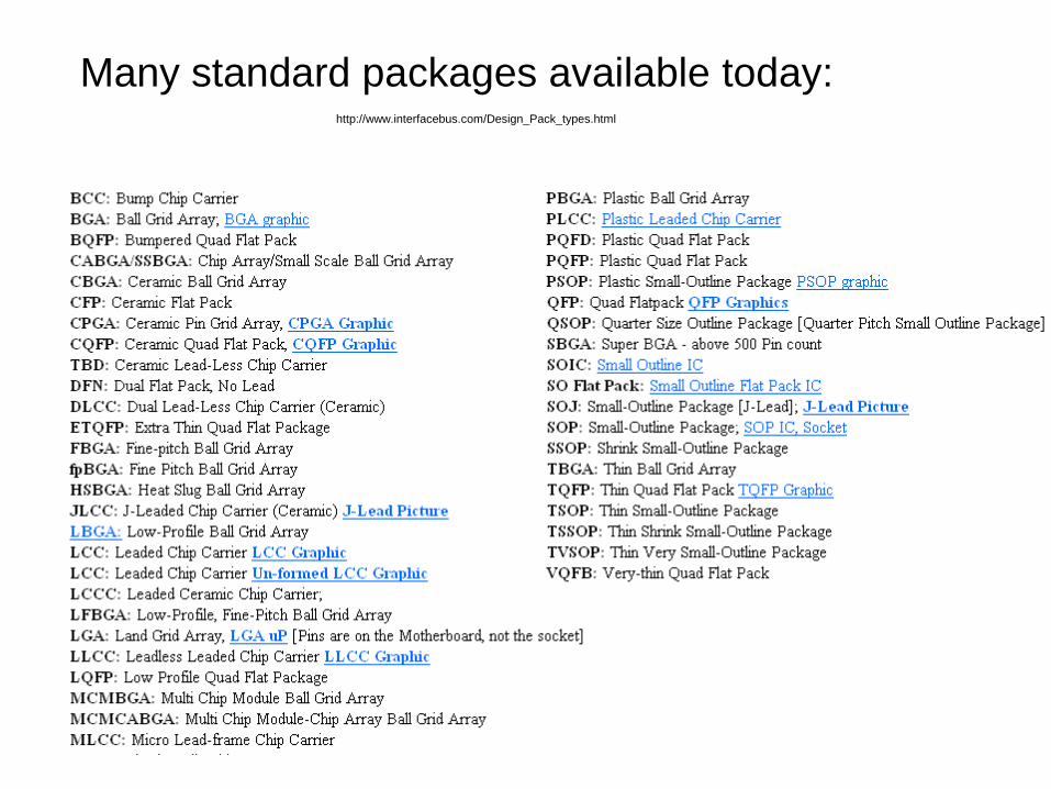
Many standard packages available today:http://www.interfacebus.com/Design_Pack_types.html

Considerable activity today and for years to
come on improving packaging technology
• Multiple die in a package
• Three-dimensional chip stacking
• Multiple levels of interconnect in
stacks
• Through silicon via technology
• Power and heat management
• Cost driven and cost constrained

Back-End Process Flow
Wafer Probe
Die Attach
Wafer Dicing
Wire Attach (bonding)
Package
Test
Ship

Testing of Integrated Circuits
Most integrated circuits are tested twice
• Wafer Probe Testing
• Packaged Part Testing
– Quick test for functionality
– Usually does not include much parametric testing
– Relatively fast and low cost test
– Package costs often quite large
– Critical to avoid packaging defective parts
– Testing costs for packaged parts can be high
– Extensive parametric tests done at package level for many
parts
– Data sheet parametrics with Max and Min values are
usually tested on all Ics
– Data sheet parametrics with Typ values are seldom tested
– Occasionally require testing at two or more temperatures
but this is costly
– Critical to avoid packaging defective parts
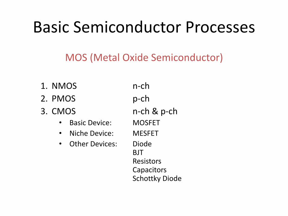
Basic Semiconductor Processes
MOS (Metal Oxide Semiconductor)
1. NMOS n-ch
2. PMOS p-ch
3. CMOS n-ch & p-ch• Basic Device: MOSFET
• Niche Device: MESFET
• Other Devices: DiodeBJTResistorsCapacitorsSchottky Diode

Basic Semiconductor Processes
1. T2L
2. ECL
3. I2L
4. Linear ICs– Basic Device: BJT (Bipolar Junction Transistor)
– Niche Devices: HBJT (Heterojunction Bipolar Transistor)HBT
– Other Devices: DiodeResistorCapacitor
Schottky DiodeJFET (Junction Field Effect Transistor)
Bipolar

Basic Semiconductor Processes
• Thin and Thick Film Processes– Basic Device: Resistor
• BiMOS or BiCMOS– Combines both MOS & Bipolar Processes– Basic Devices: MOSFET & BJT
• SiGe– BJT with HBT implementation
• SiGe / MOS– Combines HBT & MOSFET technology
• SOI / SOS (Silicon on Insulator / Silicon on Sapphire)• Twin-Well & Twin Tub CMOS
– Very similar to basic CMOS but more optimal transistor char.
Other Processes

Devices in Semiconductor Processes• Standard CMOS Process
– MOS Transistors• n-channel• p-channel
– Capacitors– Resistors– Diodes– BJT ( decent in some processes)
• npn• pnp
– JFET (in some processes)• n-channel• p-channel
• Standard Bipolar Process– BJT
• npn• pnp
– JFET • n-channel• p-channel
– Diodes– Resistors– Capacitors
• Niche Devices– Photodetectors (photodiodes, phototransistors, photoresistors)– MESFET– HBT– Schottky Diode (not Shockley)
– MEM Devices– TRIAC/SCR– ….

Basic Devices• Standard CMOS Process
– MOS Transistors• n-channel• p-channel
– Capacitors– Resistors– Diodes– BJT (in some processes)
• npn• pnp
– JFET (in some processes)• n-channel• p-channel
• Niche Devices– Photodetectors– MESFET– Schottky Diode (not Shockley)
– MEM Devices– Triac/SCR– ….
Primary Consideration
in This Course
Some Consideration in
This Course

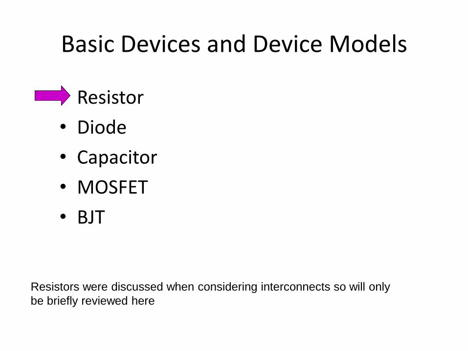
Basic Devices and Device Models
• Resistor
• Diode
• Capacitor
• MOSFET
• BJT
Basic Devices and Device Models
• Resistor
• Diode
• Capacitor
• MOSFET
• BJT
Resistors were discussed when considering interconnects so will only
be briefly reviewed here
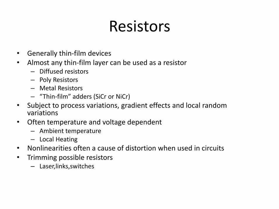
Resistors
• Generally thin-film devices• Almost any thin-film layer can be used as a resistor
– Diffused resistors– Poly Resistors– Metal Resistors– “Thin-film” adders (SiCr or NiCr)
• Subject to process variations, gradient effects and local random variations
• Often temperature and voltage dependent– Ambient temperature– Local Heating
• Nonlinearities often a cause of distortion when used in circuits• Trimming possible resistors
– Laser,links,switches

Resistor Model
V
Wd
L
I
I
VR
Model:

Resistivity
• Volumetric measure of conduction capability of a material
L
R
Area
is A
L
AR
for homogeneous
material,
A, R, Lunits : ohm cm
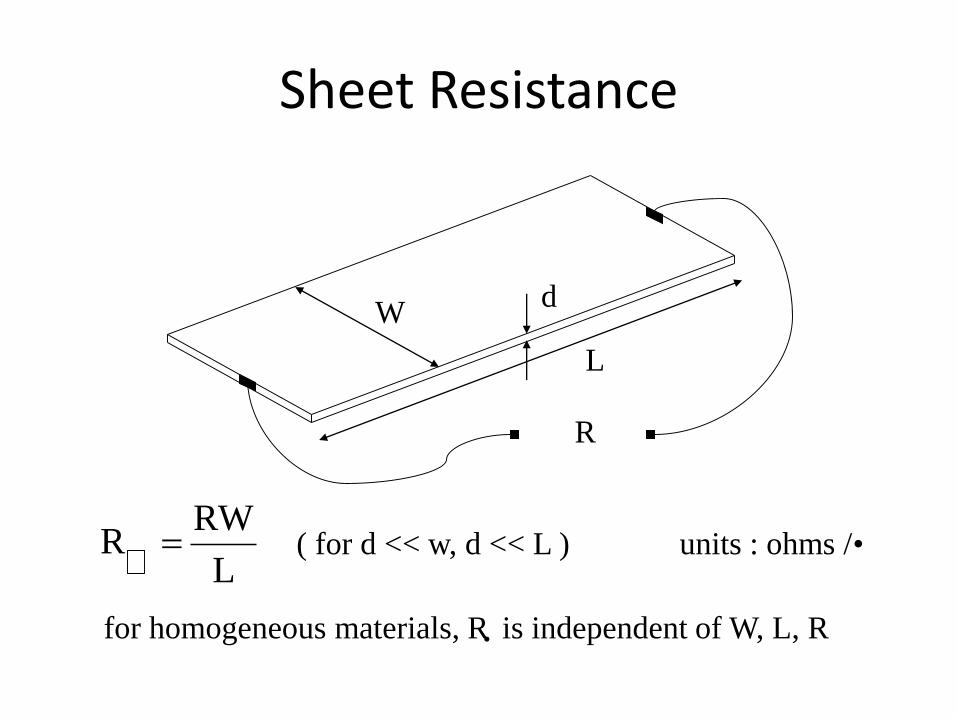
Sheet Resistance
R
Wd
L
L
RW R ( for d << w, d << L ) units : ohms / •
for homogeneous materials, R•is independent of W, L, R
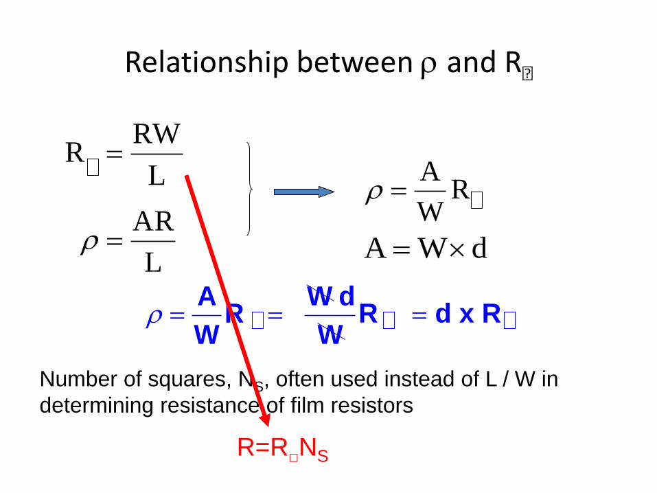
Relationship between and R•
d WA L
AR
RW
AL
RW R
RxdRW
dW R
W
A
Number of squares, NS, often used instead of L / W in
determining resistance of film resistors
R=R□NS
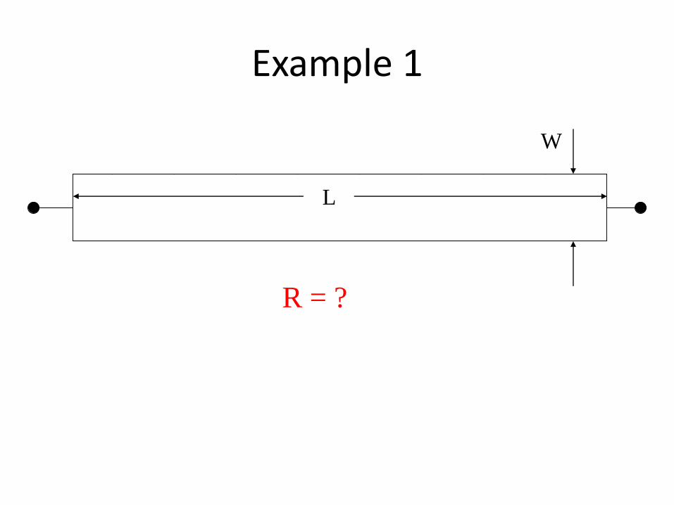
Example 1
W
R = ?
L

Example 1
W
L
SNW
L

Example 1
.4 8 7 6 5 4 3 2 1
R = ?

Example 1
.4 8 7 6 5 4 3 2 1
R = R• (8.4)
R = ?
NS=8.4

Corners in Film Resistors
Rule of Thumb: .55 squares for each corner
Corner
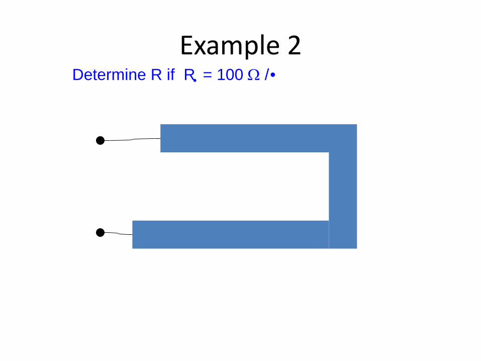
Example 2Determine R if R• = 100 / •

Example 2
1 2 3 4 5 6 .55
1 2 3 4 5 6 7 .55
1
2
3
NS=17.1
R = (17.1) R•
R = 1710

Resistivity of Materials used in Semiconductor Processing
• Cu: 1.7E-6 cm
• Al: 2.7E-4 cm
• Gold: 2.4E-6 cm
• Platinum: 3.0E-6 cm
• n-Si: .25 to 5 cm
• intrinsic Si: 2.5E5cm
• SiO2: E14 cm

Temperature Coefficients
Used for indicating temperature sensitivity of resistors & capacitors
6
op. temp
1 dRTCR 10 ppm C
R dT
This diff eqn can easily be solved if TCR is a constant
TCR
10
TT
12
6
12
TRTR
e
6121210
TCRTT1 TRTR
For a resistor:
Identical Expressions for Capacitors

Voltage Coefficients
Used for indicating voltage sensitivity of resistors & capacitors
6
ref voltage
1 dRVCR 10 ppm V
R dV
This diff eqn can easily be solved if VCR is a constant
VCR
VV
12
12
VRVR610
e
6121210
VCRVV VRVR 1
For a resistor:
Identical Expressions for Capacitors

Temperature and Voltage Coefficients
• Temperature and voltage coefficients often quite large for diffused resistors
• Temperature and voltage coefficients often quite small for poly and metal resistors

From:F. Maloberti : Design of CMOS Analog Integrated Circuits - “Resistors, Capacitors, Switches”

Example: Determine the percent change in resistance of a 5K Polysilicon
resistor as the temperature increases from 30oC to 60oC if the TCR is
constant and equal to 1500 ppm/oC
2 1 2 1 61
10
TCRR T R T T T
2 1 6
2 1
15001 30
10
1 .045
oR T R T C
R T R T
Thus the resistor increases by 4.5%
End of Lecture 11
Related Documents


![EE 330 Lecture 42 - Iowa State Universityclass.ece.iastate.edu/ee330/lectures/EE 330 Lect 42 Fall 2016.pdf · EE 330 Lecture 42 Digital Circuits • Elmore Delay ... Elmore delay[1]](https://static.cupdf.com/doc/110x72/5b57fe847f8b9a4e1b8b664d/ee-330-lecture-42-iowa-state-330-lect-42-fall-2016pdf-ee-330-lecture-42-digital.jpg)
