EE 330 Lecture 36 Digital Circuit Design • Basic Logic Gates • Properties of Logic Families • Characterization of CMOS Inverter

Welcome message from author
This document is posted to help you gain knowledge. Please leave a comment to let me know what you think about it! Share it to your friends and learn new things together.
Transcript

EE 330
Lecture 36
Digital Circuit Design
• Basic Logic Gates
• Properties of Logic Families
• Characterization of CMOS Inverter

Exam 3 Friday Nov 6
Final Mon Nov 23 (scheduled 2:15 pm)
Exams 2 and 3 will be posted on Canvas by 9:00 AM on the day of
exam and due at 1:00 PM
Final Exam will be posted on Canvas by 10:00 AM on the day of exam
and due at 4:15 PM
???
???

White pad

Types of Capacitors in MOSFETs
1. Fixed Capacitors
a. Fixed Geometry
b. Junction
2. Operating Region Dependent
Review from Last Lecture
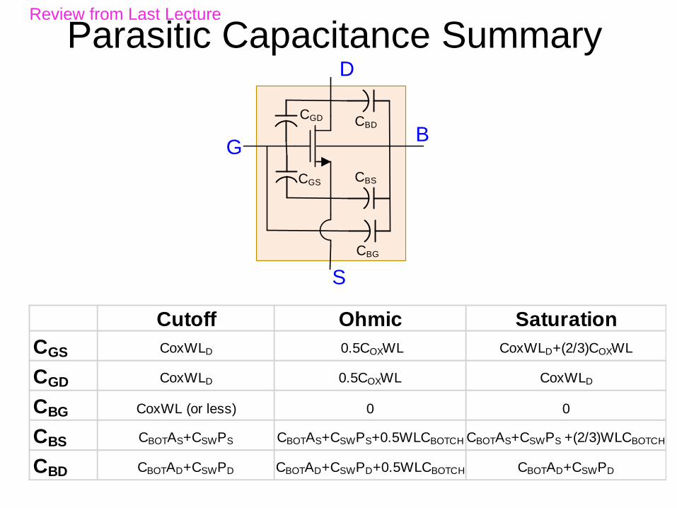
Parasitic Capacitance Summary
Cutoff Ohmic Saturation
CGS CoxWLD 0.5COXWL CoxWLD+(2/3)COXWL
CGD CoxWLD 0.5COXWL CoxWLD
CBG CoxWL (or less) 0 0
CBS CBOTAS+CSWPS CBOTAS+CSWPS+0.5WLCBOTCH CBOTAS+CSWPS +(2/3)WLCBOTCH
CBD CBOTAD+CSWPD CBOTAD+CSWPD+0.5WLCBOTCH CBOTAD+CSWPD
CGS
CGD CBD
CBS
CBG
GB
D
S
Review from Last Lecture

Parasitic Capacitance Summary
CGS
CGD CBD
CBS
CBG
GB
D
S
CGS
CGD CBD
CBS
CBG
GB
D
S
High Frequency Large Signal Model High Frequency Small Signal Model
Often VBS=0 and CBG=0, so simplifies to
CGS
CGD CBD
G
B
D
S
CGS
CGD CBD
G
B
D
S
Review from Last Lecture

High Frequency Small-Signal Model
CGS
CGD CBD
CBS
CBG
GB
D
S
Often VBS=0 and CBG=0, so simplifies to
CGS
CGD CBD
G
B
D
S
Vgs gmVgsCDBCGS
CGD
gmbVbsgo
Vbs CSB
CGB
G
B
D
S
4-terminal low frequency model
4-terminal high frequency model
Vgs gmVgsCDBCGS
CGD
go
G D
S,B3-terminal low frequency model
3-terminal high frequency model (with VBS=0)
Review from Last Lecture

High Frequency Small-Signal ModelOften VBS=0 and CBG=0 and CGD and g0 can be neglected so simplifies farther to
CGS
CBD
G
B
D
S
Vgs gmVgsCDBCGS
G D
S,B3-terminal low frequency model
3-terminal high frequency model (with VBS=0) neglecting CGD
Neglecting CGD which is high frequency feedback from output to input
often simplifies analysis considerably
Review from Last Lecture

Small-signal and simplified dc equivalent elements
C
Large
C
Small
L
Large
L
Small
C
L
Simplified
Simplified
Capacitors
Inductors
MOS
transistors
Diodes
Simplified
Element ss equivalentSimplified dc
equivalent
(MOSFET (enhancement or
depletion), JFET)
Recall:
Have not yet considered situations where the small capacitor is
relevant in small-signal analysis
Review from Last Lecture

Amplifiers with Small Capacitors
1OUT DB D m INsC G g V V
1OUT m
IN DB D
g
sC G
V
V
Solving:
Equivalently:
Causes gain to decrease at high frequencies
Consider parasitic CGS and CDB
1
1OUT m D
IN DB D
g R
sC R
V
V
By KCL:
VA
ω
Vgs gm1Vgs
Vout
RDCDBVIN
CGS
M1
Vin
Vout
-VSS
VDD
RD
CDB
Review from Last Lecture
(since impedance of CDB= )1
DBsC
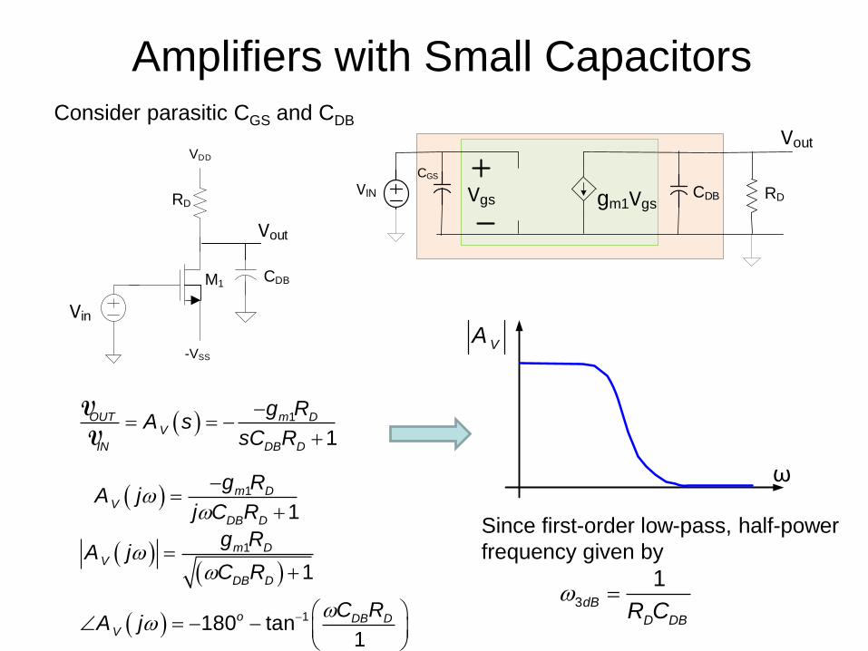
Amplifiers with Small CapacitorsConsider parasitic CGS and CDB
1
1OUT m D
V
IN DB D
g RA s
sC R
V
V
VA
ω
Vgs gm1Vgs
Vout
RDCDBVIN
CGS
M1
Vin
Vout
-VSS
VDD
RD
CDB
1
1m D
V
DB D
g RA j
j C R
1
1
1
180 tan1
m DV
DB D
o DB DV
g RA j
C R
C RA j
Since first-order low-pass, half-power
frequency given by
3
1dB
D DBR C

Sinusoidal Steady State Response for Linear Systems
If VIN=Vmsin(ωt+θ) where Vm is small (so linear operation maintained)
Steady state output is also a sinusoid given by
sinOUT m V VV t V A j t A j
Key Result from EE 201
VA sVIN(t) VOUT(t)

Sinusoidal Steady State Response for Linear Systems
M1
Vin
Vout
-VSS
VDD
RD
CDB
1
2
1
1
180 tan1
m DV
DB D
o DB DV
g RA j
C R
C RA j
If VIN=Vmsin(ωt+θ)
11
2sin 180 tan
11
om D DB DOUT m
DB D
g R C RV t V t
C R
For Vm small, small-signal steady state output given by

Digital Circuit DesignMost of the remainder of the course will be devoted to
digital circuit design
F
A
B
AB
C
C
F
3.5V
M6 M4M5
M3
M2
M1
module gates (input logic [3:0] a,b,
output logic [3:0] y1,y2,y3,y4,y5);
assign y1 = a&b; //AND
assign y2 = a | b; //OR
assign y3 = a ^ b; //XOR
assign y4 = ~(a & b); //NAND
assign y5 = ~( a | b); //NOR
endmodule
Verilog
library IEEE; use IEEE.STD_LOGIC_1164.all;
entity gates is
port(a,b: in STD_LOGIC_VECTOR(3 dowto 0);
y1,y2,y3,y4,y5:out STD_LOGIC_VECTOR(3 downto 0));
end;
architecture synth of gates is
begin
y1 <= a and b;
y2 <= a or b;
y3 <= a xor b;
y4 <= a nand b;
y5 <= a nor b;
end;
VHDL
A rendering of a small standard
cell with three metal layers
(dielectric has been removed).
The sand-colored structures are
metal interconnect, with the
vertical pillars being contacts,
typically plugs of tungsten. The
reddish structures are polysilicon
gates, and the solid at the bottom
is the crystalline silicon bulkStandard Cell Library

Digital Circuit Design• Hierarchical Design
• Basic Logic Gates
• Properties of Logic Families
• Characterization of CMOS
Inverter
• Static CMOS Logic Gates
– Ratio Logic
• Propagation Delay
– Simple analytical models• FI/OD
• Logical Effort
– Elmore Delay
• Sizing of Gates
– The Reference Inverter
• Propagation Delay with
Multiple Levels of Logic
• Optimal driving of Large
Capacitive Loads
• Power Dissipation in Logic
Circuits
• Other Logic Styles
• Array Logic
• Ring Oscillators

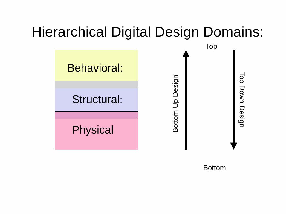
Hierarchical Digital Design Domains:
Behavioral:
Structural:
Top
Bottom
Physical
Multiple Levels of Abstraction
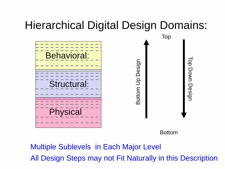
Hierarchical Digital Design Domains:
Behavioral:
Structural:
Top
Bottom
Physical Bott
om
Up D
esig
n
Top D
ow
n D
esig
n
Hierarchical Digital Design Domains:Top
BottomB
ott
om
Up D
esig
n
Top D
ow
n D
esig
n
Behavioral:
Structural:
Physical
Multiple Sublevels in Each Major Level
All Design Steps may not Fit Naturally in this Description

Behavioral : Describes what a system does or what it should do
Structural : Identifies constituent blocks and describes how these
blocks are interconnected and how they interact
Physical : Describes the constituent blocks to both the
transistor and polygon level and their physical
placement and interconnection
Hierarchical Digital Design Domains:
Multiple representations often exist at any level or sublevel

Example: Two distinct representations at the physical level (polygon sublevel)
Poly Poly
active
active
active
Poly Poly
active

Example: Two distinct representations at physical level (schematic sublevel)
W 4L
W 4
L 1
W 8
L 2
W1, LW2, L W1 + W2, L

Example: Three distinct representations at the structural/behavioral level (gate
sublevel)
A
B
C
A
B
C
cA
B
C A B
AB BA
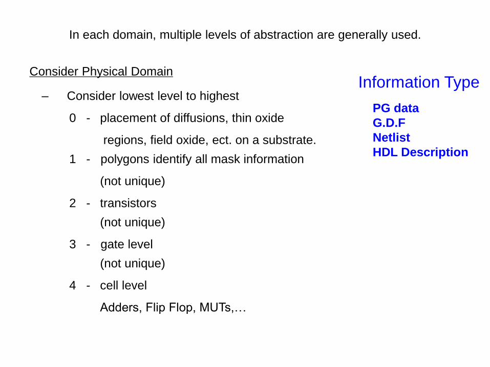
In each domain, multiple levels of abstraction are generally used.
Consider Physical Domain
– Consider lowest level to highest
0 - placement of diffusions, thin oxide
regions, field oxide, ect. on a substrate.
1 - polygons identify all mask information
(not unique)
2 - transistors
(not unique)
3 - gate level
(not unique)
4 - cell level
Adders, Flip Flop, MUTs,…
PG data
G.D.F
Netlist
HDL Description
Information Type

Structural Domain:
– DSP
– Blocks (Adders, Memory, Registers, etc.
– Gates
– Transistor
HDL
Netlists
Information Type

Behavior Domain (top down):
– Application
– Programs
– Subroutines
– Boolean Expressions
High-Level Language
HDL
Information Type

Representation of Digital Systems
Standard Approach to Digital Circuit Design
1. Behavioral Description
– Technology independent
2. RTL Description (Register Transfer Level)
(must verify (1) (2))
3. RTL Compiler
Registers and Combinational Logic Functions
4. Logic Optimizer
5. Logic Synthesis
Generally use a standard call library for synthesis
(sublevels 6-8 not shown on this slide)
8 – level representation

Representation of Digital Systems
Standard Approach to Digital Circuit Design
1. Behavioral Description
– Technology independent
2. RTL Description
(must verify (1) (2))
3. RTL Compiler
Registers and Combinational Logic Functions
4. Logic Optimizer
5.Logic Synthesis
Generally use a standard call library for synthesis
HDL
Frontend design
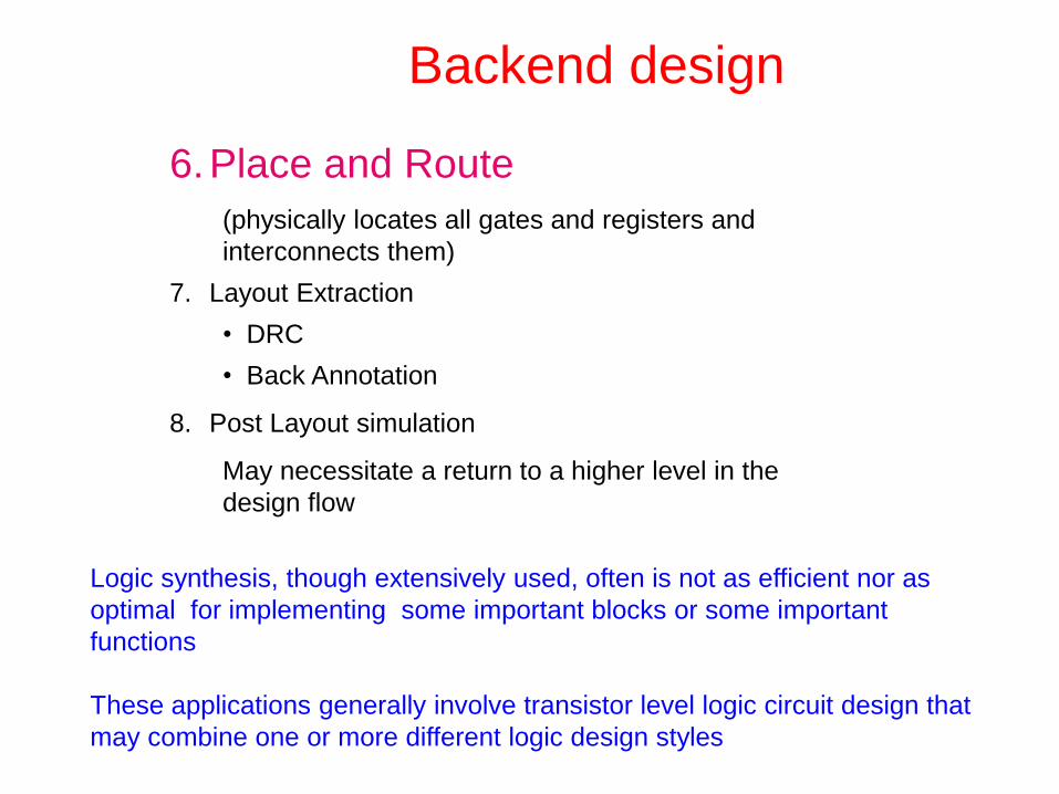
6.Place and Route
(physically locates all gates and registers and
interconnects them)
7. Layout Extraction
• DRC
• Back Annotation
8. Post Layout simulation
May necessitate a return to a higher level in the
design flow
Logic synthesis, though extensively used, often is not as efficient nor as
optimal for implementing some important blocks or some important
functions
These applications generally involve transistor level logic circuit design that
may combine one or more different logic design styles
Backend design

Logic Optimization
• Number of Gates
• Number or Levels of Logic
• Speed
• Delay
• Power Dissipation
• Area
• Cost
• Peak Current
What is optimized (or minimized) ?
Depends Upon What User Is Interested In

Standard Cell Library
• Set of primitive building blocks that have been pre-characterized for dc and high frequency performance
• Generally includes basic multiple-input gates and flip flops
• P-cells often included
• Can include higher-level blocks– Adders, multipliers, shift registers,counters,…
• Cell library often augmented by specific needs of a group or customer

Digital Circuit Design• Hierarchical Design
• Basic Logic Gates
• Properties of Logic Families
• Characterization of CMOS
Inverter
• Static CMOS Logic Gates
– Ratio Logic
• Propagation Delay
– Simple analytical models• FI/OD
• Logical Effort
– Elmore Delay
• Sizing of Gates
– The Reference Inverter
• Propagation Delay with
Multiple Levels of Logic
• Optimal driving of Large
Capacitive Loads
• Power Dissipation in Logic
Circuits
• Other Logic Styles
• Array Logic
• Ring Oscillators
done
partial

Logic Circuit Block Design
Many different logic design styles
•Static Logic Gates
•Complex Logic Gates
•Pseudo NMOS
•Pass Transistor Logic
•Dynamic Logic Gates
•Domino Logic
•Zipper Logic
•Output Prediction
Logic
Various logic design styles often combined in the
implementation of one logic block

The basic logic gates
X
X
Y
Y
Y
Y
Y
Y
Y
Y
A
A
A
A
A
A
B
B
B
B
B
B
XY
XY
BAY
BAY
BAY
BAY
BAY
BAY
AOIA
B
C
D
OAIA
B
C
D
Y
Y
A1
An
Y
A1
An
Y
A1
AnY
A1
AnY
DCBAY
DCBAY
n21 ...AAAY
n21 ...AAAY
n21 ...AAAY
n21 ...AAAY

The basic logic gatesX
X
Y
Y
Y
Y
A
AB
B
XY
XY
BAY
BAY
Y
Y
Y
Y
A
A
A
A
B
B
B
BBAY
BAY
BAY
BAY
Question: How many basic one and two input gates exist and how many
of these are useful?

The set of NOR gates is complete
Any combinational logic function can be realized with only multiple-input NOR gates
The set of NAND gates is completeAny combinational logic function can be realized with
only multiple-input NAND gates
Performance of the BASIC gates is critical!
The basic logic gates
The basic logic gates
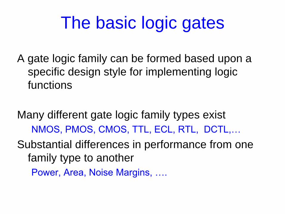
A gate logic family can be formed based upon a
specific design style for implementing logic
functions
Many different gate logic family types exist
NMOS, PMOS, CMOS, TTL, ECL, RTL, DCTL,…
Substantial differences in performance from one
family type to another
Power, Area, Noise Margins, ….

The basic logic gates
It suffices to characterize the inverter of a logic
family and then express the performance of
other gates in that family in terms of the
performance of the inverter.
What characteristics are required and desirable for an inverter to form the
basis for a useful logic family?

What restrictions are there on the
designer for building Boolean circuits?
• None !!!!
• It must “work” as expected
• Designer is Master of the silicon !

Desirable and/or Required Logic
Family Characteristics
What are the desired characteristics of a logic family?
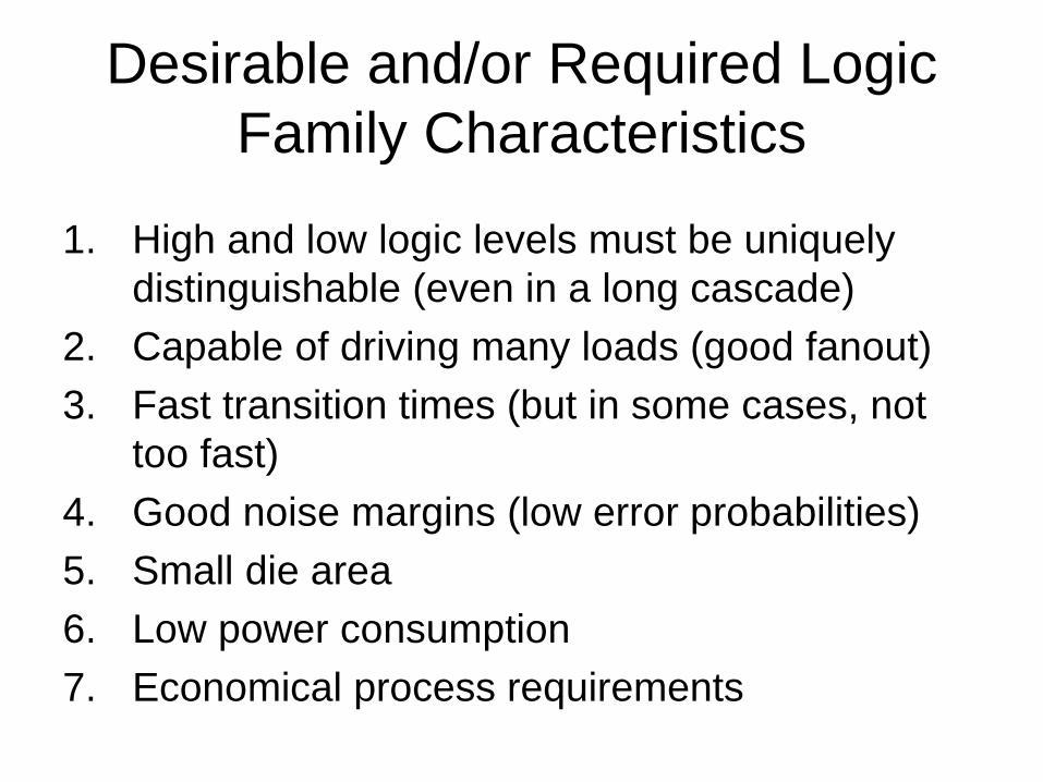
Desirable and/or Required Logic
Family Characteristics
1. High and low logic levels must be uniquely
distinguishable (even in a long cascade)
2. Capable of driving many loads (good fanout)
3. Fast transition times (but in some cases, not
too fast)
4. Good noise margins (low error probabilities)
5. Small die area
6. Low power consumption
7. Economical process requirements

Desirable and/or Required Logic
Family Characteristics
8. Minimal noise injection to substrate
9. Low leakage currents
10. No oscillations during transitions
11. Compatible with synthesis tools
12. Characteristics do not degrade too much with temperature
13. Characteristics do not vary too much with process variations
Are some of these more important than others?
Yes ! – must have well-defined logic levels for
circuits to even function as logic

Desirable and/or Required Logic
Family Characteristics
Are some of these more important than others?
Yes ! – must have well-defined logic levels for circuits
to even function as logic
What are the logic levels for a given inverter of for a
given logic family?
What properties of an inverter are necessary for it to be
useful for building a logic family

What are the logic levels for a given inverter of for a given
logic family?
VH=? VL=?
Can we legislate them ?• Some authors choose to simply define a value for them
• Simple and straightforward approach
• But what if the circuit does not interpret them the same way
they are defined !!

What are the logic levels for a given inverter of for a given
logic family?
VH=? VL=?
Can we legislate them ?

What are the logic levels for a given inverter of for a given
logic family?
VH=?
VL=?Can we legislate them ?
World’s most widely used electronics text

What are the logic levels for a given inverter of for a given
logic family?
VH=?
VL=?Can we legislate them ?

What are the logic levels for a given inverter of for a given
logic family?
VH=? VL=?
Can we legislate them ?• Some authors choose to define them based upon specific features of inverter
• Analytical expressions may be complicated
• But what if the circuit does not interpret them the same way they are defined !!
VOUT
VIN
VL VH

What are the logic levels for a given inverter of for a given
logic family?
VH=? VL=?
Ask the inverter how it will interpret logic levels• The inverter will interpret them the way the circuit really operate as a
Boolean system !!
• Analytical expressions may be complicated
• How is this determination made?VOUT
VIN

Ask the inverter how it will interpret logic levels
VH=?
VL=?
VOUT
VIN
VIN VOUT
VLARGE V? V?V? V?V?V? V? V? V?
Consider a very long cascade of inverters
Apply a large voltage at the input (alternatively a small input could be used)
w.l.o.g. assume an even number of inverters in chain indicated
even number of stages

Ask the inverter how it will interpret logic levels
VH=?
VL=?
VOUT
VIN
VIN VOUT
VLARGE VH VHVL VLVLV? V? V? VL VHor
Consider a very long cascade of inverters
Apply a large voltage at the input (alternatively a small input could be used)
w.l.o.g. assume an even number of inverters in chain indicated
even number of stages
If logic levels are to be maintained, the voltage at the end of this even
number of stages must be VH, that of the next must be VL, the next VH, etc.
until the start of the cascade is approached
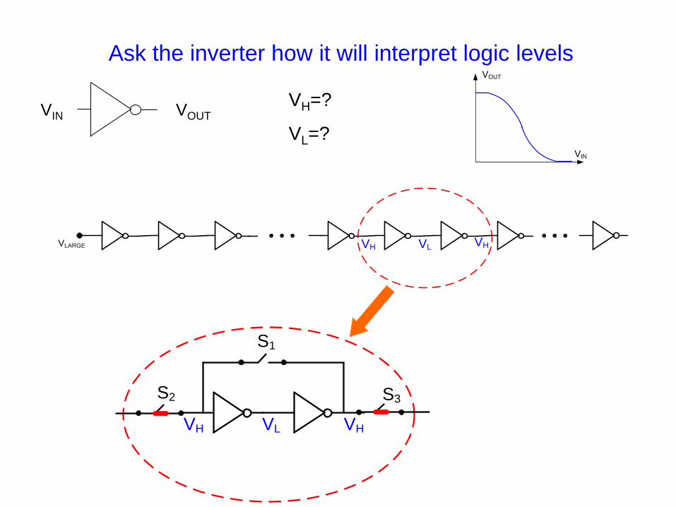
Ask the inverter how it will interpret logic levels
VH=?
VL=?
VOUT
VIN
VIN VOUT
VLARGE VH VHVL
S1
S2 S3
VH VHVL

Ask the inverter how it will interpret logic levels
VH=?
VL=?
VOUT
VIN
S1
S2 S3
VH VHVL
S1
S2 S3
VH VHVL
S1
S2 S3
VH VHVL

Ask the inverter how it will interpret logic levels
VH=?
VL=?
VOUT
VIN
S1
S2 S3
VH VHVL
• Two inverter loop
• Very useful circuit !

Stay Safe and Stay Healthy !

End of Lecture 36
?
What Characteristics of a Logic Family are Desirable?
Student List:
• Speed
• Power
• Size
• Cost
• Good Noise Margin
• Signal Swing
• Input Capacitance
• Output Impedance (drive capability)
• Well-Defined Logic Levels
Related Documents