DRONACHARYA GROUP OF INSTITUTIONS, GREATER NOIDA Affiliated to Mahamaya Technical University, Noida Approved by AICTE DEPARTMENT OF INFORMATION TECHNLOGY Lab Manual for Microprocessor Lab EEC-456

Welcome message from author
This document is posted to help you gain knowledge. Please leave a comment to let me know what you think about it! Share it to your friends and learn new things together.
Transcript
DRONACHARYA GROUP OF INSTITUTIONS, GREATER NOIDA
Affiliated to Mahamaya Technical University, Noida Approved by AICTE
DEPARTMENT OF INFORMATION TECHNLOGY
Lab Manual for Microprocessor Lab EEC-456
Syllabus
EEC-456 : MICROPROCESSOR LAB L T P 0 0 2
1. To study 8085 microprocessor System 2. To study 8086 microprocessor System 3. To develop and run a programme to find out largest and smallest number 4. To develop and run a programme for converting temperature from F to C degree 5. To develop and run a programme to compute square of a given number 6. To develop and run a programme for computing ascending/descending order of a number. 7. To perform interfacing of RAM chip to 8085/8086 8. To perform interfacing of keyboard controller 9. To perform interfacing of DMA controller 10. To perform interfacing of UART/USART
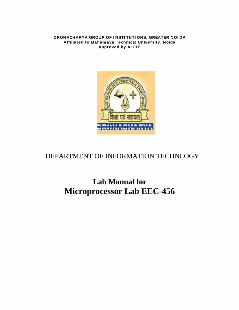
Aim : 1 To study 8085 microprocessor System Intel 8085 is an 8-bit, N-channel Metal Oxide semiconductor (NMOS) microprocessor It is a 40 pin IC package fabricated on a single Large Scale Integration (LSI) chip The Intel 8085 uses a single +5V DC supply for its operation Its clock speed is about 3MHz The clock cycle is of 320 ns The time for the clock cycle of the Intel 8085 is 200 ns It has 80 basic instructions and 246 opcodes
Address and Data Bus Address Bus The 8085 has eight signal lines, A15-A8, which are unidirectional and used as the high
order address bus Multiplexed Address/Data Bus The signal lines AD7-AD0 are bidirectional They serve a dual purpose
They are used as the low-order address bus as well as the data bus In executing an instruction, during the earlier part of the cycle, these lines are used as the low-
order address bus as well as the data bus During the later part of the cycle, these lines are used as the data bus However the low order address bus can be separated from these signals by using a latch
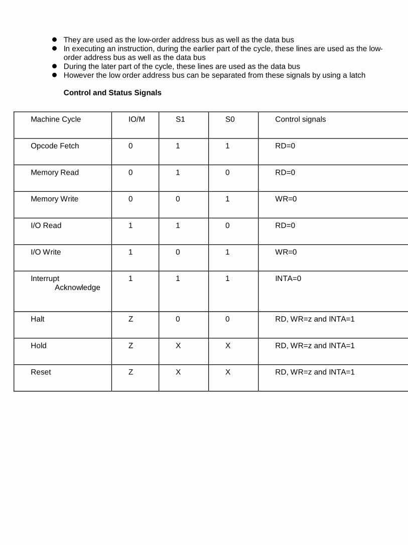
Control and Status Signals
Machine Cycle IO/M S1 S0 Control signals
Opcode Fetch 0 1 1 RD=0
Memory Read 0 1 0 RD=0
Memory Write 0 0 1 WR=0
I/O Read 1 1 0 RD=0
I/O Write 1 0 1 WR=0
Interrupt Acknowledge
1 1 1 INTA=0
Halt Z 0 0 RD, WR=z and INTA=1
Hold Z X X RD, WR=z and INTA=1
Reset Z X X RD, WR=z and INTA=1
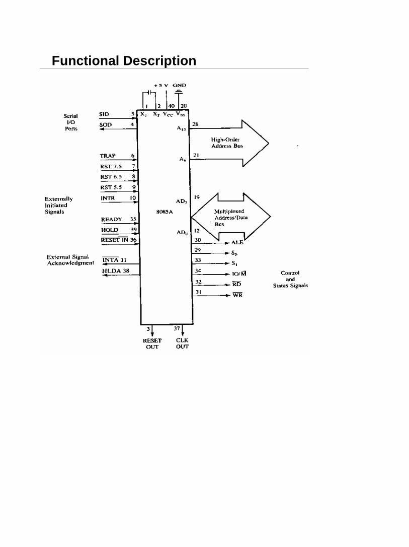
Functional Description
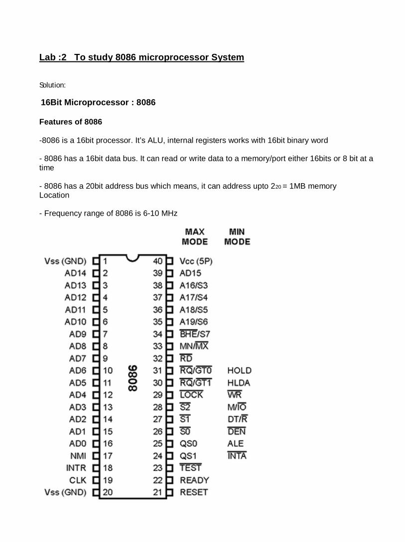
Lab :2 To study 8086 microprocessor System Solution:
16Bit Microprocessor : 8086 Features of 8086 -8086 is a 16bit processor. It’s ALU, internal registers works with 16bit binary word - 8086 has a 16bit data bus. It can read or write data to a memory/port either 16bits or 8 bit at a time - 8086 has a 20bit address bus which means, it can address upto 220 = 1MB memory Location - Frequency range of 8086 is 6-10 MHz

Important 8086 Pin Diagram/Description AD15±AD0 ADDRESS DATA BUS: These lines constitute the time multiplexed memory/IO address and data bus. ALE Address Latch Enable. A HIGH on this line causes the lower order 16bit address bus to be latched that stores the addresses and then, the lower order 16bit of the address bus can be used as data bus. READY READY is the acknowledgement from the addressed memory or I/O device that it will complete the data transfer. INTR INTERRUPT REQUEST: is a level triggered input which is sampled during the last clock cycle of each instruction to determine if the processor should enter into an interrupt acknowledge operation. A subroutine is vectored to via an interrupt vector lookup table located in system memory. It can be internally masked by software resetting the interrupt enable bit. INTR is internally synchronized. This signal is active HIGH. INTA Interrupt Acknowledge from the MP
NMI NON-MASKABLE INTERRUPT: an edge triggered input which causes an interrupt request to the MP. A subroutine is vectored to via an interrupt vector lookup table located in system memory. NMI is not maskable internally by software. RESET: causes the processor to immediately terminate its present activity. The signal must be active HIGH for at least four clock cycles. It restarts execution MN/MX MINIMUM/MAXIMUM: indicates what mode the processor is to operate in. The two modes are discussed in the following sections. M/IO : Differentiate between the Memory and I/O operation. A LOW on this pin indicated I/O operation and a HIGH indicated a Memory Operation HOLD : The 8086 has a pin called HOLD. This pin is used by external devices to gain control of the busses. HLDA : When the HOLD signal is activated by an external device, the 8086 stops executing instructions and stops using the busses. This would allow external devices to control the information
8086 MINIMUM AND MAXIMUM MODES of operation
MN/MX Minimum mode The 8086 processor works in a single processor environment. All control signals for memory and I/O are generated by the microprocessor. Maximum mode is designed to be used when a coprocessor exists in the system. 8086 works in a multiprocessor environment. Control signals for memory and I/O are generated by an external BUS Controller.
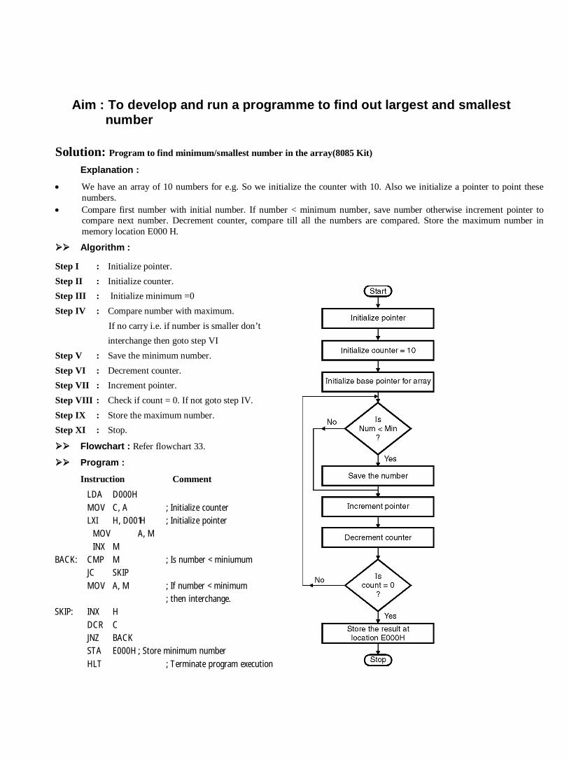
Aim : To develop and run a programme to find out largest and smallest number
Solution: Program to find minimum/smallest number in the array(8085 Kit)
Explanation :
We have an array of 10 numbers for e.g. So we initialize the counter with 10. Also we initialize a pointer to point these numbers.
Compare first number with initial number. If number < minimum number, save number otherwise increment pointer to compare next number. Decrement counter, compare till all the numbers are compared. Store the maximum number in memory location E000 H.
Algorithm :
Step I : Initialize pointer. Step II : Initialize counter. Step III : Initialize minimum =0 Step IV : Compare number with maximum. If no carry i.e. if number is smaller don’t interchange then goto step VI Step V : Save the minimum number. Step VI : Decrement counter. Step VII : Increment pointer. Step VIII : Check if count = 0. If not goto step IV. Step IX : Store the maximum number. Step XI : Stop.
Flowchart : Refer flowchart 33. Program :
Instruction Comment LDA D000H MOV C, A ; Initialize counter LXI H, D001H ; Initialize pointer MOV A, M INX M BACK: CMP M ; Is number < miniumum JC SKIP MOV A, M ; If number < minimum ; then interchange. SKIP: INX H DCR C JNZ BACK STA E000H ; Store minimum number HLT ; Terminate program execution
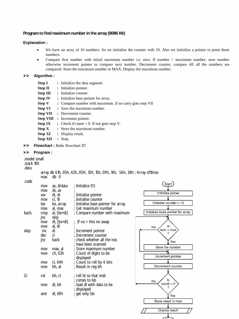
Program to find maximum number in the array (8086 Kit)
Explanation :
We have an array of 10 numbers. So we initialize the counter with 10. Also we initialize a pointer to point these numbers.
Compare first number with initial maximum number i.e. zero. If number > maximum number, save number otherwise increment pointer to compare next number. Decrement counter, compare till all the numbers are compared. Store the maximum number in MAX. Display the maximum number.
Algorithm :
Step I : Initialize the data segment. Step II : Initialize pointer. Step III : Initialize counter. Step IV : Initialize base pointer for array. Step V : Compare number with maximum. If no carry goto step VII Step VI : Save the maximum number. Step VII : Decrement counter. Step VIII : Increment pointer. Step IX : Check if count = 0. If not goto step V. Step X : Store the maximum number. Step XI : Display result. Step XII : Stop.
Flowchart : Refer flowchart 37. Program : .model small .stack 100 .data array db 61h, 05h, 42h, 05H, 12H, 15h, 09h, 14h, 56h, 38h ; Array of10nos max db 0 .code mov ax, @data ; Initialize DS mov ds, ax ; xor di, di ; Initialise pointer mov cl, 10 ; Initialise counter lea bx, array ; Initialise base pointer for array mov al, max ; Get maximum number back: cmp al, [bx+di] ; Compare number with maximum jnc skip mov dl, [bx+di] ; If no > this no swap mov al, dl ; skip: inc di ; Increment pointer dec cl ; Decrement counter jnz back ; check whether all the nos ; have been scanned mov max, al ; Store maximum number mov ch, 02h ; Count of digits to be ; displayed mov cl, 04h ; Count to roll by 4 bits mov bh, al ; Result in reg bh l2: rol bh, cl ; roll bl so that msb ; comes to lsb mov dl, bh ; load dl with data to be ; displayed and dl, 0fH ; get only lsb
cmp dl, 09 ; check if digit is 0-9 ; or letter A-F jbe l4 add dl, 07 ; if letter add 37H ; else only add 30H l4: add dl, 30H mov ah, 02 ; Function 2 under ; INT 21H ; (Display character) int 21H dec ch ; Decrement Count jnz l2 mov ah, 4cH ; Terminate Program int 21H end
Flowchart 37
Result :
C:\programs>tasm maxno.asm Turbo Assembler Version 3.0 Copyright (c) 1988, 1991 Borland International Assembling file: maxno.asm Error messages: None Warning messages: None Passes: 1 Remaining memory: 437k C:\programs>tlink maxno.obj Turbo Link Version 3.0 Copyright (c) 1987, 1990 Borland International C:\programs>maxno
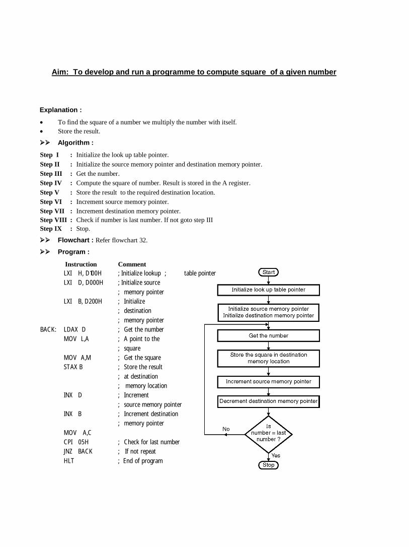
Aim: To develop and run a programme to compute square of a given number
Explanation :
To find the square of a number we multiply the number with itself. Store the result.
Algorithm :
Step I : Initialize the look up table pointer. Step II : Initialize the source memory pointer and destination memory pointer. Step III : Get the number. Step IV : Compute the square of number. Result is stored in the A register. Step V : Store the result to the required destination location. Step VI : Increment source memory pointer. Step VII : Increment destination memory pointer. Step VIII : Check if number is last number. If not goto step III Step IX : Stop.
Flowchart : Refer flowchart 32. Program :
Instruction Comment LXI H, D100H ; Initialize lookup ; table pointer LXI D, D000H ; Initialize source ; memory pointer LXI B, D200H ; Initialize ; destination ; memory pointer BACK: LDAX D ; Get the number MOV L,A ; A point to the ; square MOV A,M ; Get the square STAX B ; Store the result ; at destination ; memory location INX D ; Increment ; source memory pointer INX B ; Increment destination ; memory pointer MOV A,C CPI 05H ; Check for last number JNZ BACK ; If not repeat HLT ; End of program
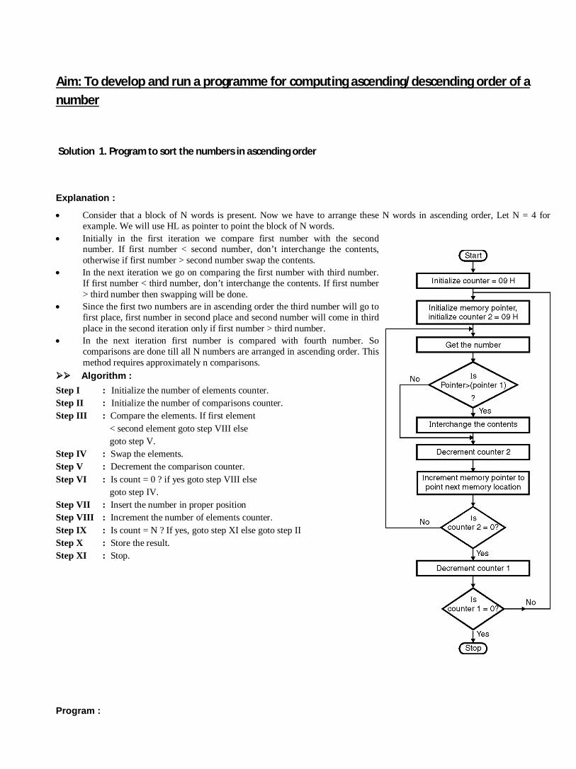
Aim: To develop and run a programme for computing ascending/descending order of a number
Solution 1. Program to sort the numbers in ascending order
Explanation :
Consider that a block of N words is present. Now we have to arrange these N words in ascending order, Let N = 4 for example. We will use HL as pointer to point the block of N words.
Initially in the first iteration we compare first number with the second number. If first number < second number, don’t interchange the contents, otherwise if first number > second number swap the contents.
In the next iteration we go on comparing the first number with third number. If first number < third number, don’t interchange the contents. If first number > third number then swapping will be done.
Since the first two numbers are in ascending order the third number will go to first place, first number in second place and second number will come in third place in the second iteration only if first number > third number.
In the next iteration first number is compared with fourth number. So comparisons are done till all N numbers are arranged in ascending order. This method requires approximately n comparisons.
Algorithm : Step I : Initialize the number of elements counter. Step II : Initialize the number of comparisons counter. Step III : Compare the elements. If first element < second element goto step VIII else goto step V. Step IV : Swap the elements. Step V : Decrement the comparison counter. Step VI : Is count = 0 ? if yes goto step VIII else goto step IV. Step VII : Insert the number in proper position Step VIII : Increment the number of elements counter. Step IX : Is count = N ? If yes, goto step XI else goto step II Step X : Store the result. Step XI : Stop.
Program :
Instruction Comment
MVI B, 09 ; Initialize counter 1
START: LXI H, D000H ; Initialize memory pointer
MVI C, 09H ; Initialize counter 2
BACK: MOV A, M ; Get the number in accumulator
INX H ; Increment memory pointer
CMP M ; Compare number with next number
JC SKIP ; If less, don’t interchange
JZ SKIP ; If equal, don’t interchange
MOV D, M ; Otherwise swap the contents
MOV M, A
DCX H ; Interchange numbers
MOV M, D
INX H ; Increment pointer to next memory location
SKIP: DCR C ; Decrement counter 2
JNZ BACK ; If not zero, repeat
DCR B ; Decrement counter 1
JNZ START ; If not zero, repeat HLT ; Terminate program execution
Solution 2 : Program to sort the numbers in descending order Explanation :
Consider that a block of N words is present.
Now we have to arrange these N numbers in descending order, Let N = 4 for example.
We will use HL as pointer to point the block of N numbers.
Initially in the first iteration we compare the first number with the second number. If first number > second number don’t interchange the contents. If first number < second number swap their contents. Now at the end of this iteration first two elements are sorted in descending order.
In the next iteration we will compare the first number along with third. If first > third don’t interchange contents otherwise swap the contents. At the end of this iteration first three elements are sorted in descending order. Go on comparing till all the elements are arranged in descending order. This method requires approximately n comparisons.
Algorithm :
Step I : Initialize the number of elements counter.
Step II : Initialize the number of comparisons counter.
Step III : Compare the elements.
If first element > second element goto step VIII else goto step V.
Step IV : Swap the elements.
Step V : Decrement the comparison counter.
Step VI : Is count = 0 ? If yes, goto step VIII else goto step IV.
Step VII : Insert the number in proper position.
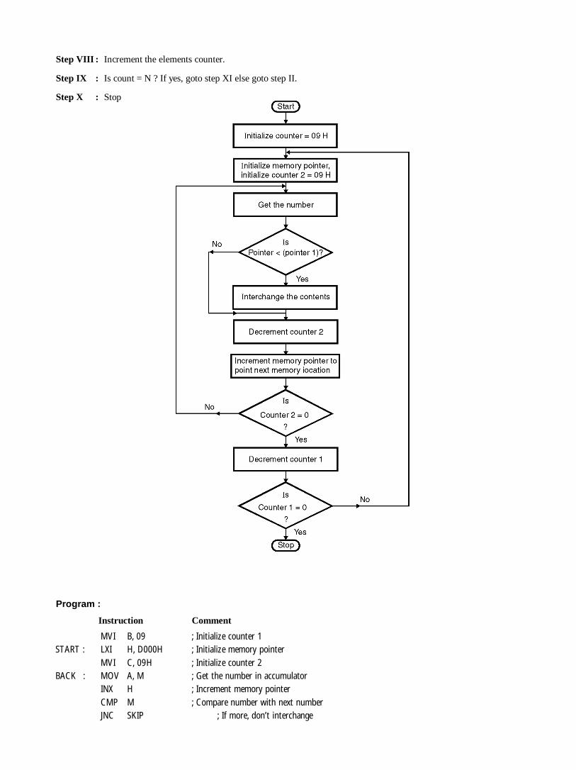
Step VIII : Increment the elements counter.
Step IX : Is count = N ? If yes, goto step XI else goto step II.
Step X : Stop
Program : Instruction Comment
MVI B, 09 ; Initialize counter 1 START : LXI H, D000H ; Initialize memory pointer MVI C, 09H ; Initialize counter 2 BACK : MOV A, M ; Get the number in accumulator INX H ; Increment memory pointer CMP M ; Compare number with next number JNC SKIP ; If more, don’t interchange
JZ SKIP ; If equal, don’t interchange MOV D, M ; Otherwise swap the contents MOV M, A DCX H ; Interchange numbers MOV M, D INX H ; Increment pointer to next memory location SKIP: DCR C ; Decrement counter 2 JNZ BACK ; If not zero, repeat DCR B ; Decrement counter 1 JNZ START ; If not zero, repeat HLT ; Terminate program execution
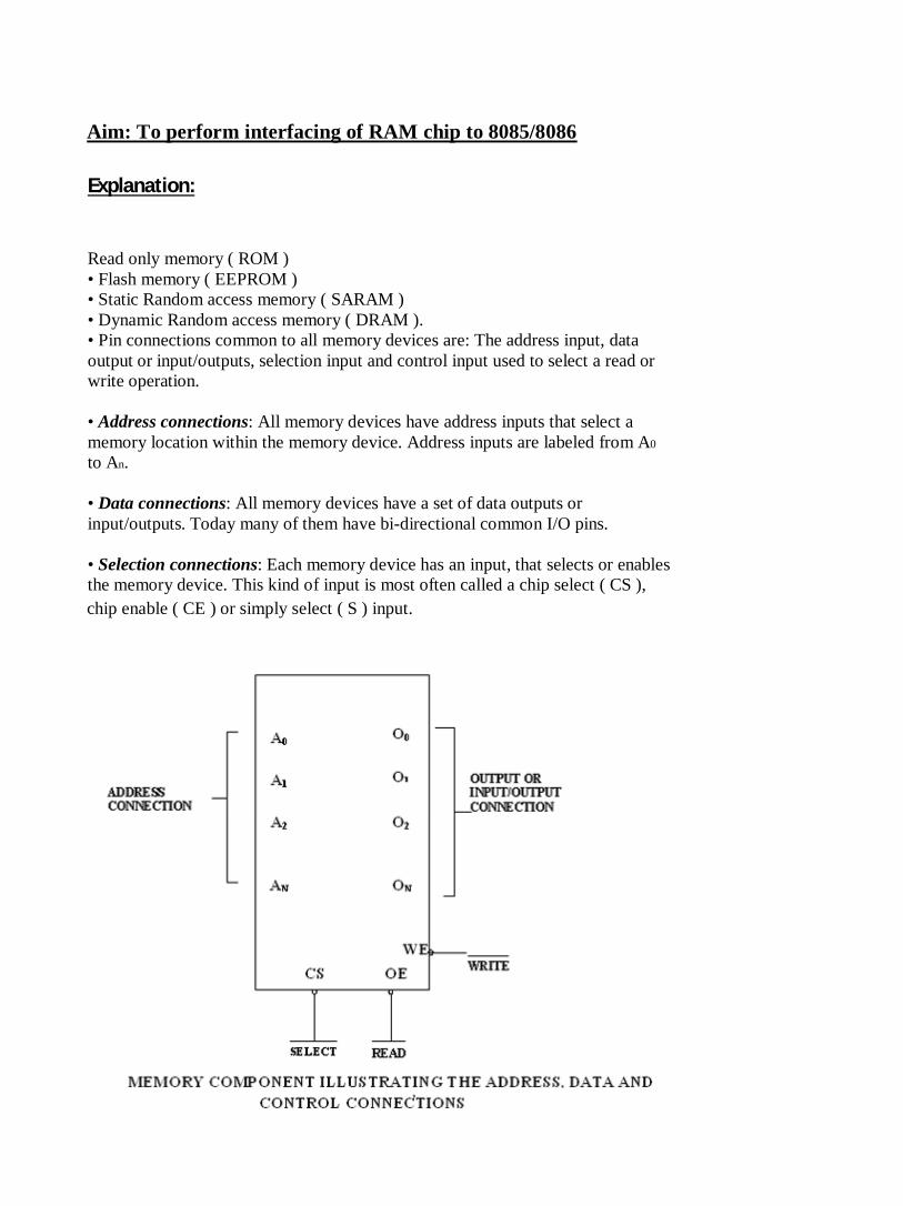
Aim: To perform interfacing of RAM chip to 8085/8086 Explanation: Read only memory ( ROM ) • Flash memory ( EEPROM ) • Static Random access memory ( SARAM ) • Dynamic Random access memory ( DRAM ). • Pin connections common to all memory devices are: The address input, data output or input/outputs, selection input and control input used to select a read or write operation. • Address connections: All memory devices have address inputs that select a memory location within the memory device. Address inputs are labeled from A0
to An. • Data connections: All memory devices have a set of data outputs or input/outputs. Today many of them have bi-directional common I/O pins. • Selection connections: Each memory device has an input, that selects or enables the memory device. This kind of input is most often called a chip select ( CS ), chip enable ( CE ) or simply select ( S ) input.
RAM memory generally has at least one CS or S input and ROM at least one CE . • If the CE , CS, S input is active the memory device perform the read or write. • If it is inactive the memory device cannot perform read or write operation. • If more than one CS connection is present, all most be active to perform read or write data. • Control connections: A ROM usually has only one control input, while a RAM often has one or two control inputs. • The control input most often found on the ROM is the output enable ( OE ) or gate ( G ), this allows data to flow out of the output data pins of the ROM. • If OE and the selected input are both active, then the output is enable, if OE is inactive, the output is disabled at its high-impedance state. • The OE connection enables and disables a set of three-state buffer located within the memory device and must be active to read data. • A RAM memory device has either one or two control inputs. If there is one control input it is often called R/W. • This pin selects a read operation or a write operation only if the device is selected by the selection input ( CS ). If the RAM has two control inputs, they are usually labeled WE or W and OE or G . • ( WE ) write enable must be active to perform a memory write operation and OE must be active to perform a memory read operation. • When these two controls WE and OE are present, they must never be active at the same time. • The ROM read only memory permanently stores programs and data and data was always present, even when power is disconnected. • It is also called as nonvolatile memory. • EPROM ( erasable programmable read only memory ) is also erasable if exposed to high intensity ultraviolet light for about 20 minutes or less, depending upon the type of EPROM. • We have PROM (programmable read only memory ) • RMM ( read mostly memory ) is also called the flash memory. • The flash memory is also called as an EEPROM (electrically erasable programmable ROM), EAROM ( electrically alterable ROM ), or a NOVROM ( nonvolatile ROM ). • These memory devices are electrically erasable in the system, but require more
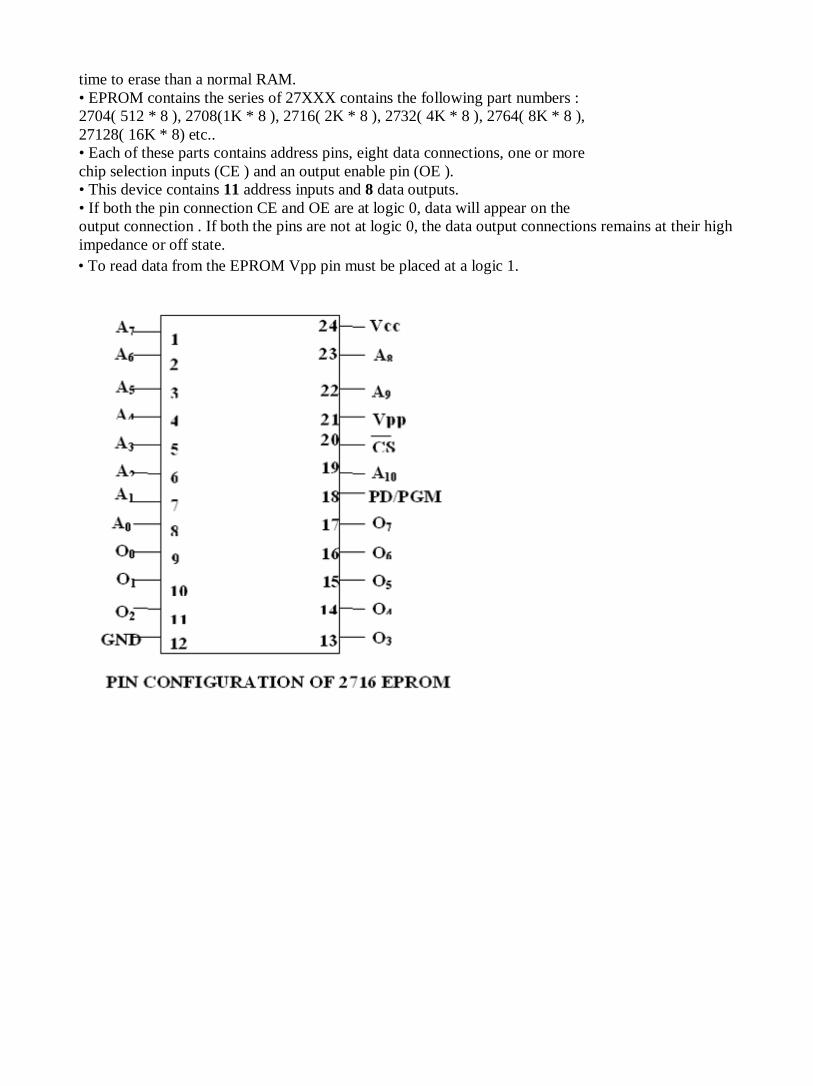
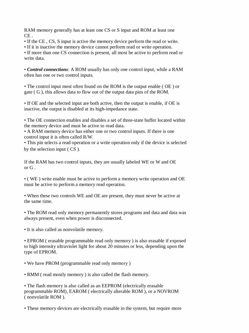
time to erase than a normal RAM. • EPROM contains the series of 27XXX contains the following part numbers : 2704( 512 * 8 ), 2708(1K * 8 ), 2716( 2K * 8 ), 2732( 4K * 8 ), 2764( 8K * 8 ), 27128( 16K * 8) etc.. • Each of these parts contains address pins, eight data connections, one or more chip selection inputs (CE ) and an output enable pin (OE ). • This device contains 11 address inputs and 8 data outputs. • If both the pin connection CE and OE are at logic 0, data will appear on the output connection . If both the pins are not at logic 0, the data output connections remains at their high impedance or off state. • To read data from the EPROM Vpp pin must be placed at a logic 1.
Static RAM Interfacing • The semiconductor RAM is broadly two types – Static RAM and Dynamic RAM. • The semiconductor memories are organised as two dimensional arrays of memory locations. • For example 4K * 8 or 4K byte memory contains 4096 locations, where each locations contains 8-bit data and only one of the 4096 locations can be selected at a time. Once a location is selected all the bits in it are accessible using a group of conductors called Data bus. • For addressing the 4K bytes of memory, 12 address lines are required. • In general to address a memory location out of N memory locations, we will require at least n bits of address, i.e. n address lines where n = Log2 N. • Thus if the microprocessor has n address lines, then it is able to address at the most N locations of memory, where 2n=N. If out of N locations only P memory locations are to be interfaced, then the least significant p address lines out of the available n lines can be directly connected from the microprocessor to the memory chip while the remaining (n-p) higher order address lines may be used for address decoding as inputs to the chip selection logic. • The memory address depends upon the hardware circuit used for decoding the chip select (CS). The output of the decoding circuit is connected with the CS pin of the memory chip. • The general procedure of static memory interfacing with 8086 is briefly described as follows: 1. Arrange the available memory chip so as to obtain 16- bit data bus width. The upper 8-bit bank is called as odd address memory bank and the lower 8-bit bank is called as even address memory bank.
2. Connect available memory address lines of memory chip with those of the microprocessor and also connect the memory RD and WR inputs to the corresponding processor control signals. Connect the 16-bit data bus of the memory bank with that of the microprocessor 8086. 3. The remaining address lines of the microprocessor, BHE and A0 are used for decoding the required chip select signals for the odd and even memory banks. The CS of memory is derived from the o/p of the decoding circuit. • As a good and efficient interfacing practice, the address map of the system should be continuous as far as possible, i.e. there should not be no windows in the map and no fold back space should be allowed. • A memory location should have a single address corresponding to it, i.e. absolute decoding should be preferred and minimum hardware should be used for decoding. Dynamic RAM • Whenever a large capacity memory is required in a microcomputer system, the memory subsystem is generally designed using dynamic RAM because there are various advantages of dynamic RAM. • E.g. higher packing density, lower cost and less power consumption. A typical static RAM cell may require six transistors while the dynamic RAM cell requires only a transistors along with a capacitor. Hence it is possible to obtain higher packaging density and hence low cost units are available. • The basic dynamic RAM cell uses a capacitor to store the charge as a representation of data. This capacitor is manufactured as a diode that is reversebiased so that the storage capacitance comes into the picture. • This storage capacitance is utilized for storing the charge representation of data but the reverse-biased diode has leakage current that tends to discharge the capacitor giving rise to the possibility of data loss. To avoid this possible data loss, the data stored in a dynamic RAM cell must be refreshed after a fixed time interval regularly. The process of refreshing the data in RAM is called as Refresh cycle. • The refresh activity is similar to reading the data from each and every cell of memory, independent of the requirement of microprocessor. During this refresh period all other operations related to the memory subsystem are suspended. Hence the refresh activity causes loss of time, resulting in reduce system performance. • However keeping in view the advantages of dynamic RAM, like low power consumption, high packaging density and low cost, most of the advanced computing system are designed using dynamic RAM, at the cost of operating speed. • A dedicated hardware chip called as dynamic RAM controller is the most important part of the interfacing circuit. • The Refresh cycle is different from the memory read cycle in the following aspects. 1. The memory address is not provided by the CPU address bus, rather it is generated by a refresh mechanism counter called as refresh counter. 2. Unlike memory read cycle, more than one memory chip may be enabled at a time
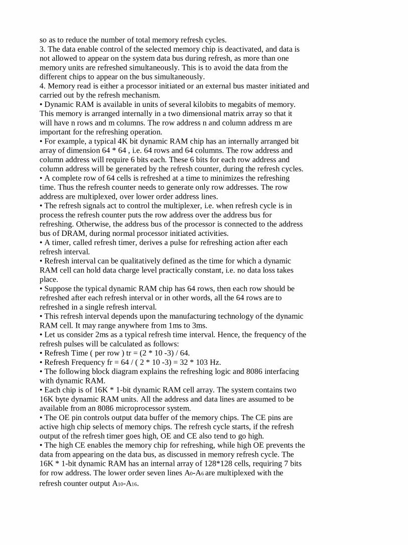
so as to reduce the number of total memory refresh cycles. 3. The data enable control of the selected memory chip is deactivated, and data is not allowed to appear on the system data bus during refresh, as more than one memory units are refreshed simultaneously. This is to avoid the data from the different chips to appear on the bus simultaneously. 4. Memory read is either a processor initiated or an external bus master initiated and carried out by the refresh mechanism. • Dynamic RAM is available in units of several kilobits to megabits of memory. This memory is arranged internally in a two dimensional matrix array so that it will have n rows and m columns. The row address n and column address m are important for the refreshing operation. • For example, a typical 4K bit dynamic RAM chip has an internally arranged bit array of dimension 64 * 64 , i.e. 64 rows and 64 columns. The row address and column address will require 6 bits each. These 6 bits for each row address and column address will be generated by the refresh counter, during the refresh cycles. • A complete row of 64 cells is refreshed at a time to minimizes the refreshing time. Thus the refresh counter needs to generate only row addresses. The row address are multiplexed, over lower order address lines. • The refresh signals act to control the multiplexer, i.e. when refresh cycle is in process the refresh counter puts the row address over the address bus for refreshing. Otherwise, the address bus of the processor is connected to the address bus of DRAM, during normal processor initiated activities. • A timer, called refresh timer, derives a pulse for refreshing action after each refresh interval. • Refresh interval can be qualitatively defined as the time for which a dynamic RAM cell can hold data charge level practically constant, i.e. no data loss takes place. • Suppose the typical dynamic RAM chip has 64 rows, then each row should be refreshed after each refresh interval or in other words, all the 64 rows are to refreshed in a single refresh interval. • This refresh interval depends upon the manufacturing technology of the dynamic RAM cell. It may range anywhere from 1ms to 3ms. • Let us consider 2ms as a typical refresh time interval. Hence, the frequency of the refresh pulses will be calculated as follows: • Refresh Time ( per row ) tr = (2 * 10 -3) / 64. • Refresh Frequency fr = 64 / ( 2 * 10 -3) = 32 * 103 Hz. • The following block diagram explains the refreshing logic and 8086 interfacing with dynamic RAM. • Each chip is of 16K * 1-bit dynamic RAM cell array. The system contains two 16K byte dynamic RAM units. All the address and data lines are assumed to be available from an 8086 microprocessor system. • The OE pin controls output data buffer of the memory chips. The CE pins are active high chip selects of memory chips. The refresh cycle starts, if the refresh output of the refresh timer goes high, OE and CE also tend to go high. • The high CE enables the memory chip for refreshing, while high OE prevents the data from appearing on the data bus, as discussed in memory refresh cycle. The 16K * 1-bit dynamic RAM has an internal array of 128*128 cells, requiring 7 bits for row address. The lower order seven lines A0-A6 are multiplexed with the refresh counter output A10-A16.
AIM: To perform interfacing of keyboard controller.
Explanation: • To give directions or data values to users, many microprocessor-controlled instruments and machines need to display letters of the alphabet and numbers. In systems where a large amount of data needs to be displayed a CRT is used to display the data. In system where only a small amount of data needs to be displayed, simple digit-type displays are often used. • There are several technologies used to make these digit-oriented displays but we are discussing only the two major types. • These are light emitting diodes (LED) and liquid-crystal displays (LCD). • LCD displays use very low power, so they are often used in portable, batterypowered instruments. They do not emit their own light, they simply change the reflection of available light. Therefore, for an instrument that is to be used in lowlight conditions, you have to include a light source for LCDs or use LEDs which emit their own light. • Alphanumeric LED displays are available in three common formats. For displaying only number and hexadecimal letters, simple 7-segment displays • To display numbers and the entire alphabet, 18 segment displays The 7- segment type is the least expensive, most commonly used and easiest to interface with, so we will concentrate first on how to interface with this type. Directly Driving LED Displays: Figure shows a circuit that you might connect to a parallel port on a microcomputer to drive a single 7-segment , common-anode display. For a common-anode display, a segment is tuned on by applying a logic low to it. • The 7447 converts a BCD code applied to its inputs to the pattern of lows required to display the number represented by the BCD code. This circuit connection is referred to as a static display because current is being passed through the display at all times. • Each segment requires a current of between 5 and 30mA to light. Let’s assume you want a current of 20mA. The voltage drop across the LED when it is lit is about 1.5V. • The output low voltage for the 7447 is a maximum of 0.4V at 40mA. So assume that it is about 0.2V at 20mA. Subtracting these two voltage drop from the supply voltage of 5V leaves 3.3V across the current limiting resistor. Dividing 3.3V by 20mA gives a value of 168Ω for the current-limiting resistor. The voltage drops across the LED and the output of 7447 are not exactly predictable and exact current through the LED is not critical as long as we don’t exceed its
Related Documents