Coarse-Grain MTCMOS Sleep Transistor Sizing Using Delay Transistor Sizing Using Delay Budgeting Ehsan Pakbaznia and Massoud Pedram University of Southern California Dept. of Electrical Engineering DATE 08 M ihG DATE-08 Munich, Germany

Welcome message from author
This document is posted to help you gain knowledge. Please leave a comment to let me know what you think about it! Share it to your friends and learn new things together.
Transcript

Coarse-Grain MTCMOS Sleep Transistor Sizing Using Delay Transistor Sizing Using Delay Budgeting
Ehsan Pakbaznia and Massoud Pedram
University of Southern CaliforniaDept. of Electrical Engineering
DATE 08 M i h GDATE-08 Munich, Germany

Leakage in CMOS TechnologyLeakage in CMOS TechnologyLeakage in CMOS TechnologyLeakage in CMOS TechnologyVdd is reduced with CMOS technology scalingVdd is reduced with CMOS technology scaling
Vth must be lowered to recover the transistor switching speedVth must be lowered to recover the transistor switching speed
The subthreshold leakage current increases exponentially with decreasing Vth
The subthreshold leakage current increases exponentially with decreasing Vth
A highly effective leakage control mechanism has proven to be the MTCMOS techniqueA highly effective leakage control mechanism has proven to be the MTCMOS technique
2
Overview of MTCMOSOverview of MTCMOSOverview of MTCMOSOverview of MTCMOSA high-Vth transistor is used to disconnect low-Vthtransistors from the ground or the supply railsA high-Vth transistor is used to disconnect low-Vthtransistors from the ground or the supply railstransistors from the ground or the supply railstransistors from the ground or the supply rails
Vdd Vdd
P
SLEEP
PVirtual Supply
High Threshold
P
N
out inLow Threshold
N
outinPpp y
N
SLEEPVirtual Ground
N
3
High Threshold
Coarse-Grain MTCMOSCoarse Grain MTCMOS
Coarse grain vs fine grain:Coarse-grain vs. fine-grain:Smaller sleep transistor areaLower leakageLower leakageRegular standard cell library can be used (no need to characterize new cells)
VDD 2
SLEEPB
TVSS
VVSS1 3 4
2
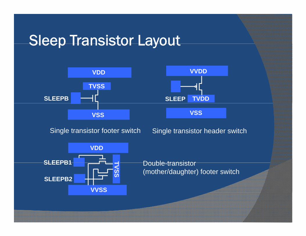
Sleep Transistor LayoutSleep Transistor Layout
VDD VVDD
SLEEPB
TVSS
VDD
SLEEP TVDD
VSS VSS
Single transistor footer switch Single transistor header switch
T
VDD
SLEEPB1
S g e t a s sto oote s tc Single transistor header switch
Double transistorTVSSVVSS
SLEEPB2
SLEEPB1 Double-transistor (mother/daughter) footer switch
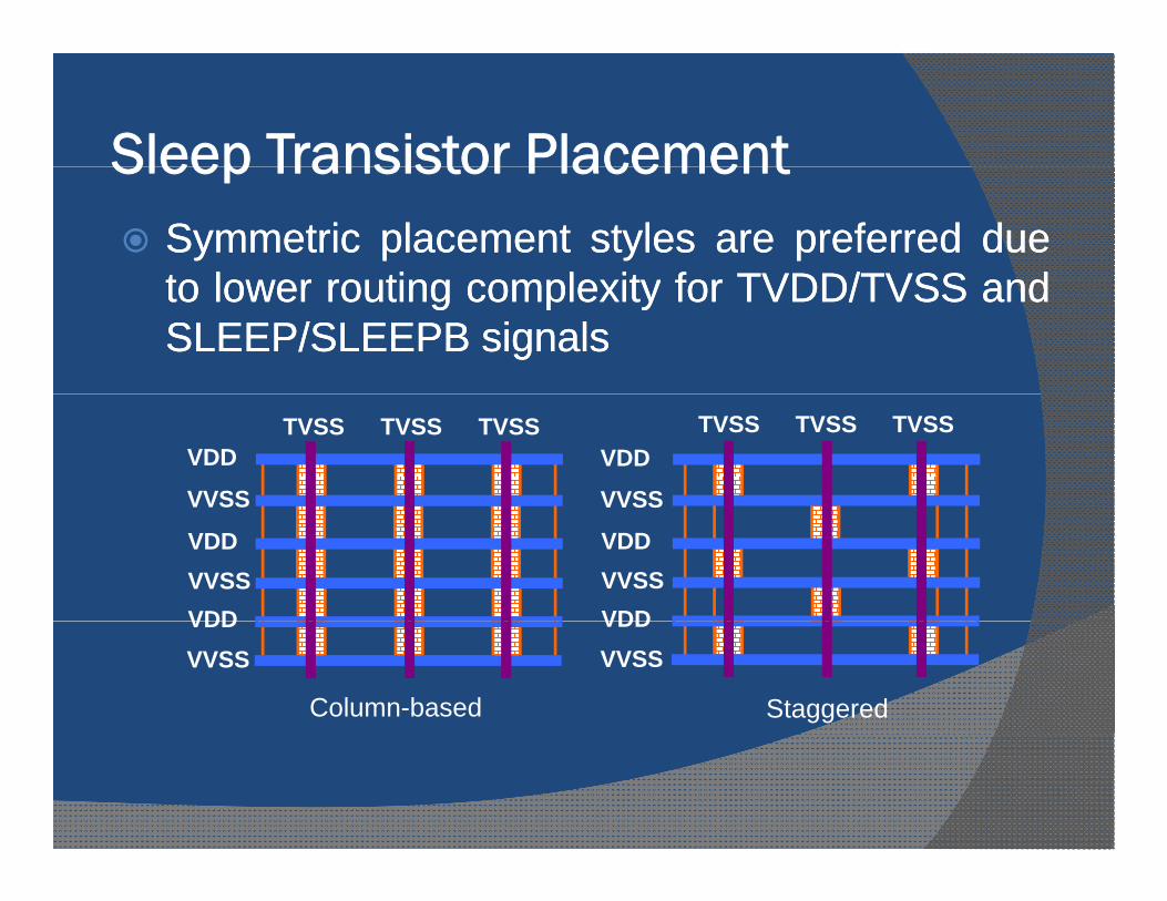
Sleep Transistor PlacementSleep Transistor PlacementSymmetric placement styles are preferred dueto lower routing complexity for TVDD/TVSS andSymmetric placement styles are preferred dueto lower routing complexity for TVDD/TVSS andto lower routing complexity for TVDD/TVSS andSLEEP/SLEEPB signalsto lower routing complexity for TVDD/TVSS andSLEEP/SLEEPB signals
VDD
VVSS
TVSS TVSS TVSSVDD
VVSS
TVSS TVSS TVSS
VDDVVSSVDD
SS
VDDVVSSVDDVDD
VVSSVDDVVSS
Column-based Staggered
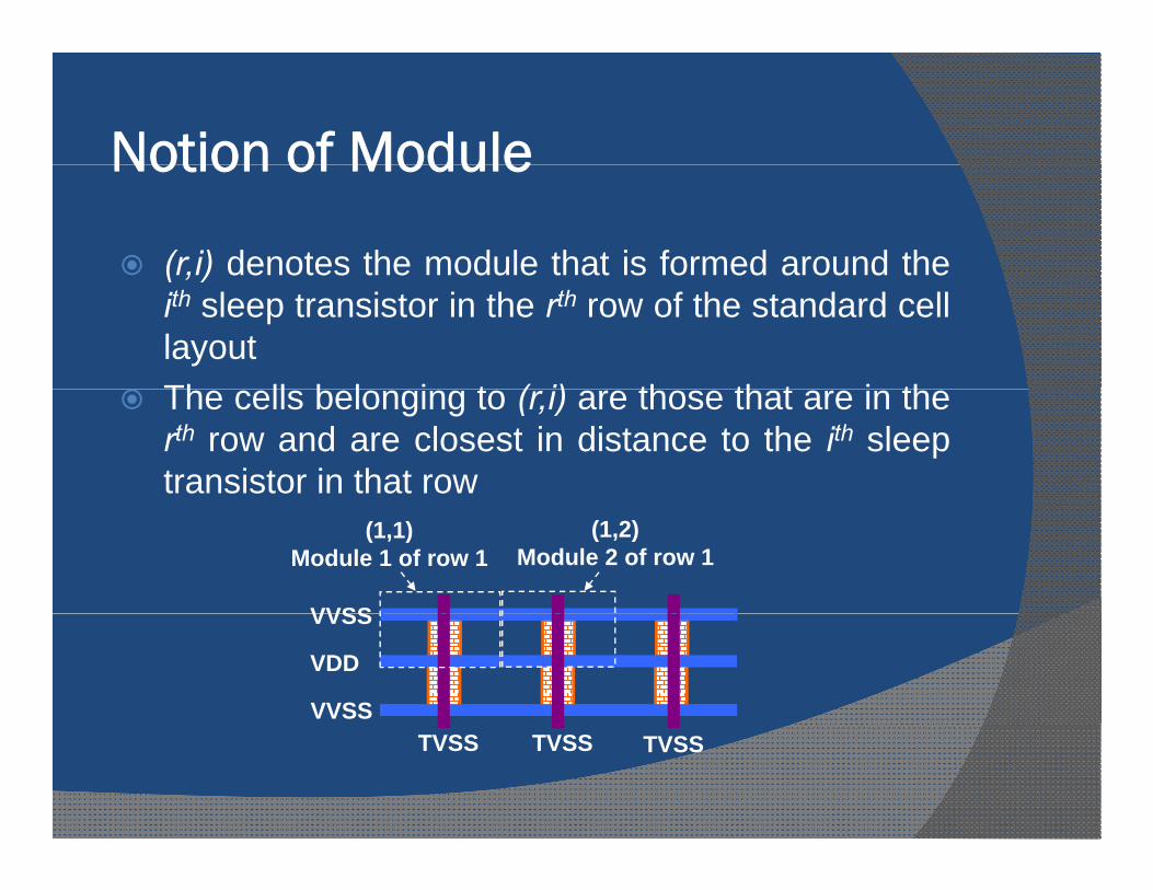
Notion of ModuleNotion of Module
(r,i) denotes the module that is formed around the( , )ith sleep transistor in the rth row of the standard celllayoutTh ll b l i t ( i) th th t i thThe cells belonging to (r,i) are those that are in therth row and are closest in distance to the ith sleeptransistor in that row
VVSS
(1,1)Module 1 of row 1
(1,2)Module 2 of row 1
VVSS
VDD
VVSSTVSS TVSS TVSS
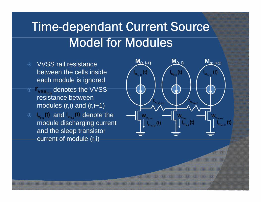
Time-dependant Current Source Model for Modules
VVSS il i t M(r i 1) M(r i) M(r i+1)VVSS rail resistance between the cells inside each module is ignored
denotes the VVSSr
M(r, i-1) (r, i) M(r, i+1)
(r,i-1)MI (t)(r,i)MI (t)
(r,i+1)MI (t)
denotes the VVSS resistance between modules (r,i) and (r,i+1)
and denote the
(r,i)VSSr
I (t) I (t)
SS(r,i)VrSS(r,i-1)Vr
and denote the module discharging current and the sleep transistor current of module (r i)
(r,i)MI (t)(r,i)stI (t)
(r,i-1)stW(r,i)stW
(r,i+1)stW
(r,i-1)stI (t) (r,i)stI (t)(r,i+1)stI (t)
current of module (r,i)
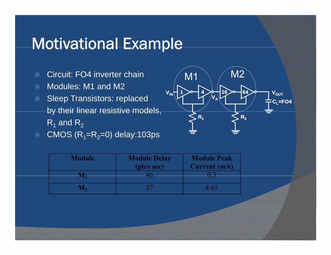
Motivational ExampleMotivational Example
Circuit: FO4 inverter chain M1 M2Modules: M1 and M2Sleep Transistors: replaced by their linear resistive models
1 4VIN VOUT
CL=FO4
16 64VA
1 4VIN VOUT
CL=FO4
16 64VA
M1
by their linear resistive models, R1 and R2
CMOS (R1=R2=0) delay:103ps
R1 R2R1 R2
Module Module Delay (pico sec)
Module Peak Current (mA)
M1 46 0 3M1 46 0.3
M2 57 4.65

Effect of Slack Distribution on Total Sleep Transistor Size
Ci iModule
D l ( )Total D l
Sleep Tx R i ∑Ri
-1 Circuit Delay (ps) Delay
(ps) Resistance
(Ω)
∑Ri(Ω-1)
CMOS TM1= 46 TM2= 57 103 R1=0
R2=0 TM1= 50.6 T 62 7 113.3 R1=250
R 9 0.1151TM2= 62.7 113.3 R2=9 0.1151
TM1= 52 TM2= 61.3 113.3 R1=330
R2=2 0.5030 MTCMOS
TM1= 48 TM2= 65.3 113.3 R1=110
R2=25 0.0491
Total available slack: 10.3ps (10% delay penalty)Case 1: uniformly distributed slack (medium)C 2 80% f M1 d 20% f M2 ( t)Case 2: 80% for M1 and 20% for M2 (worst)Case 3: 20% for M1 and 80% for M2 (best)
Current-aware optimization: must slow down modules ith l di h twith larger discharge current more
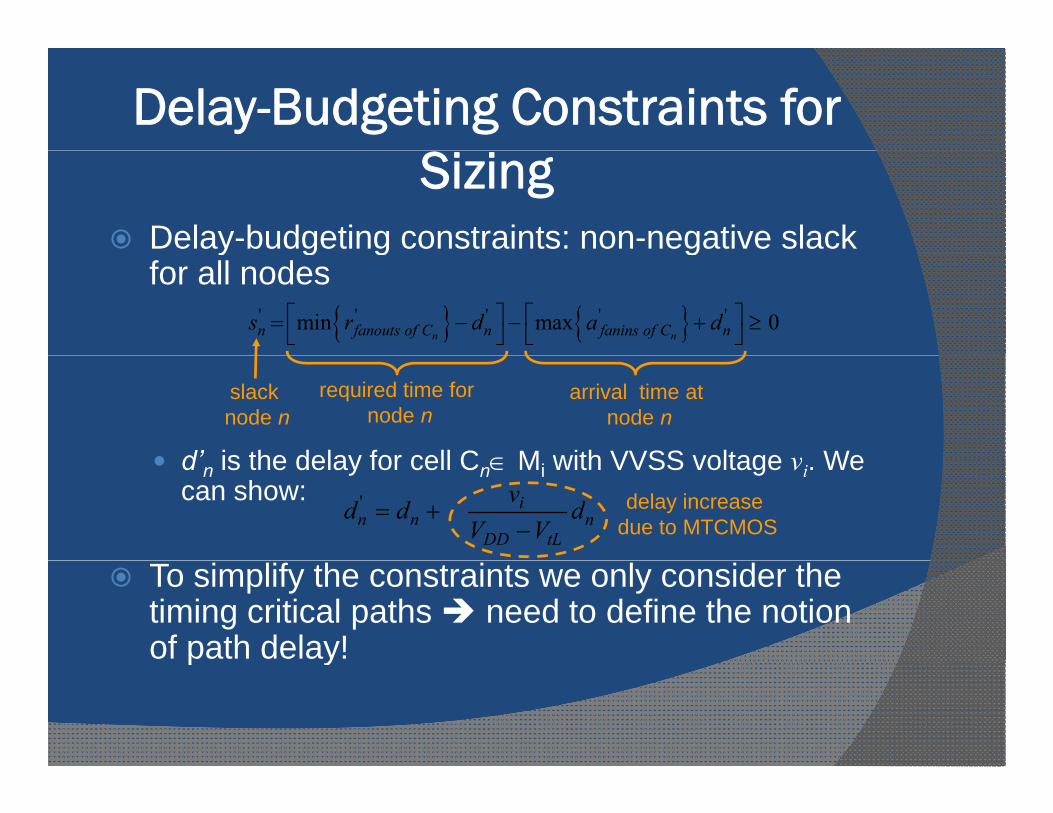
Delay-Budgeting Constraints for Sizing
Delay-budgeting constraints: non-negative slack y g g gfor all nodes
' ' ' ' 'min max 0n nn fanouts of C n fanins of C ns r d a d⎡ ⎤ ⎡ ⎤= − − + ≥
⎣ ⎦ ⎣ ⎦
d’ is the delay for cell C ∈ M with VVSS voltage v We
required time for node n
arrival time at node n
slack node n
d n is the delay for cell Cn∈ Mi with VVSS voltage vi. We can show: ' i
n n nDD tL
vd d d
V V= +
−delay increase
due to MTCMOS
To simplify the constraints we only consider the timing critical paths need to define the notion of path delay!p y
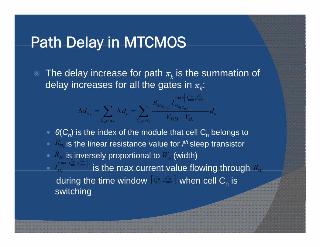
Path Delay in MTCMOSPath Delay in MTCMOS
The delay increase for path πk is the summation of y p kdelay increases for all the gates in πk:
( ) ( )
maxminmax ,
θ θ
⎡ ⎤⎣ ⎦
∑ ∑C Cn n
C Cn
t tst stR I
d d d
θ(Cn) is the index of the module that cell Cn belongs to
( ) ( )θ θ
ππ π∈ ∈
Δ = Δ =−∑ ∑ C Cn n
k
n k n k
n nDD tLC C
d d dV V
is the linear resistance value for ith sleep transistoris inversely proportional to (width)
is the max current value flowing throughmaxminmax ,⎡ ⎤⎣ ⎦
C Cn nt tstI
istR
stRistR
istW
is the max current value flowing throughduring the time window when cell Cn is switching
maxmin ,C Cn nt t⎡ ⎤⎣ ⎦
ist ist
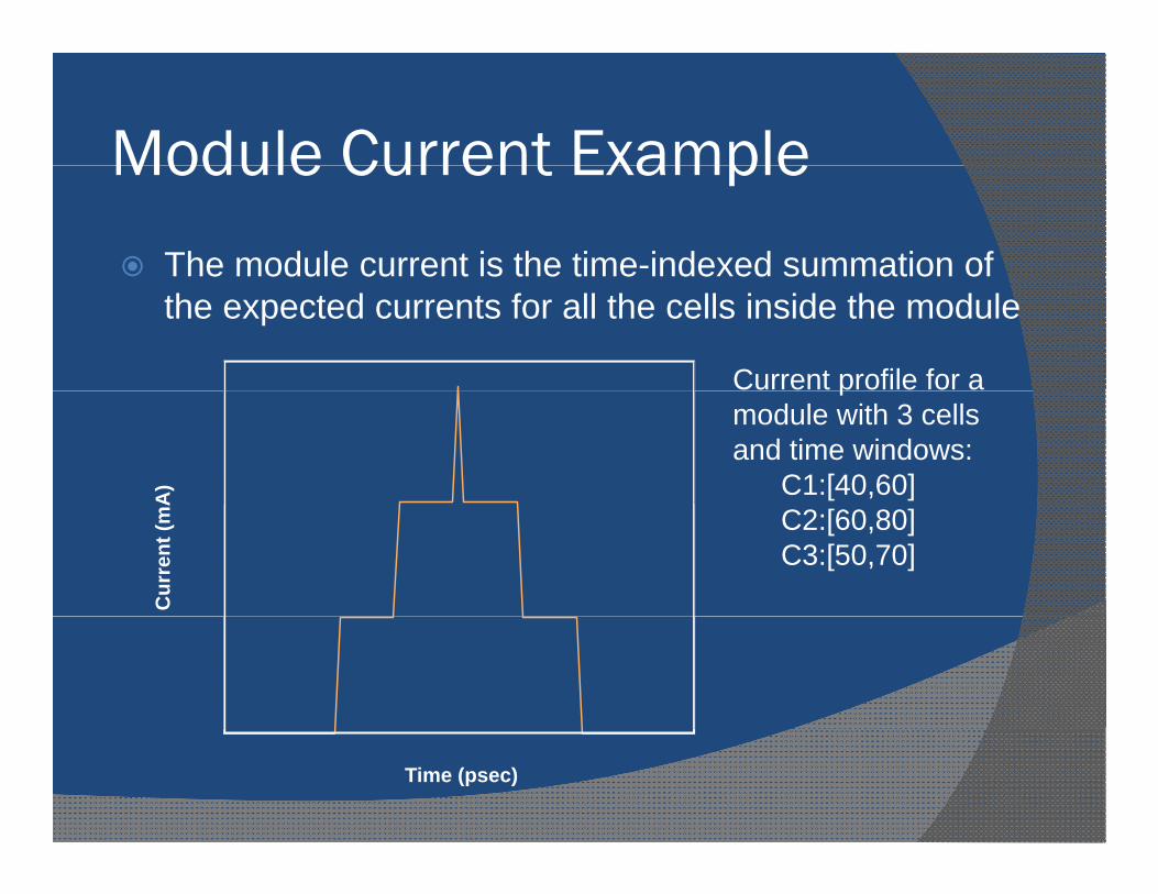
Module Current ExampleModule Current Example
The module current is the time-indexed summation of the expected currents for all the cells inside the module
0.45Current profile for a
A) 0.3
0.35
0.4p
module with 3 cells and time windows:
C1:[40,60]
Cur
rent
(mA
0.15
0.2
0.25 C2:[60,80]C3:[50,70]
0
0.05
0.1
Time (psec)20 30 40 50 60 70 80 90 100
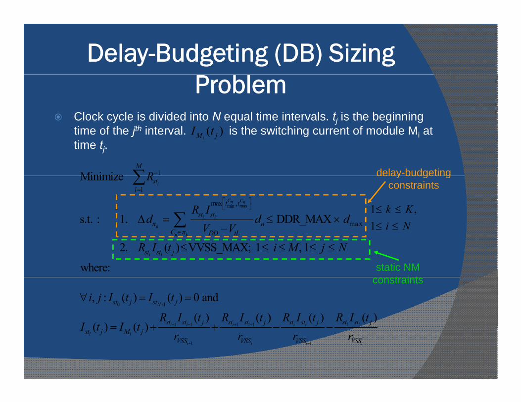
Delay-Budgeting (DB) Sizing Problem
Clock cycle is divided into N equal time intervals. tj is the beginning time of the jth interval. is the switching current of module Mi at time tj.
1MinimizeM
R−∑
( )iM jI t
delay-budgeting
maxmin
1
max ,
max
Minimize
s.t. : 1. DDR_MAX
i
C Cn n
i i
k
sti
t tst st
n
R
R Id d d
V Vπ
=
⎡ ⎤⎣ ⎦
Δ = ≤ ×
∑
∑
delay budgetingconstraints
1 ,1
k Ki N
≤ ≤≤ ≤
2. ( ) VVSS_MAX; 1 , 1
where:
k
n k
i i
C DD tL
st st j
V VR I t i M j N
π∈ −
≤ ≤ ≤ ≤ ≤
∑
static NMt i t
1 i N≤ ≤
0 1
1 1
, : ( ) ( ) 0 and
( )( ) ( )
N
i i
st j st j
st st j
i j I t I t
R I t RI t I t
+
− −
∀ = =
= + + 1 1( ) ( ) ( )
i i i i i ist st j st st j st st jI t R I t R I t+ + − −
constraints
1
( ) ( )i i
i
st j M jVSS
I t I tr
−
= + +1i i iVSS VSS VSSr r r−

BCM and MCMBCM and MCM
The delay-budgeting constraints can be written as:M
Definition 1- At any given step of the sizing algorithm, the
ma x1
DDR_MAX ; 1i
M
ki sti
a R d k K=
≤ × ≤ ≤∑
most critical module (MCM) is the module with the maximum delay contribution in the K most critical paths:
arg maxi
K
ki stMCM a R= ∑Definition 2- At any given step of the sizing algorithm thebest candidate module (BCM) is defined as the modulewhose sleep transistor upsizing by a certain percentage will
1i
i
ki stM k=
∑
whose sleep transistor upsizing by a certain percentage willresult in the largest delay improvement for unsatisfied paths.One can show:
( )| 1 DDR MAXBCM MCM k K d dΔ ( )| 1 , DDR_MAXk kkBCM MCM k K d dπ ππ= ≤ ≤ Δ >
Current-Aware OptimizationCurrent Aware Optimization
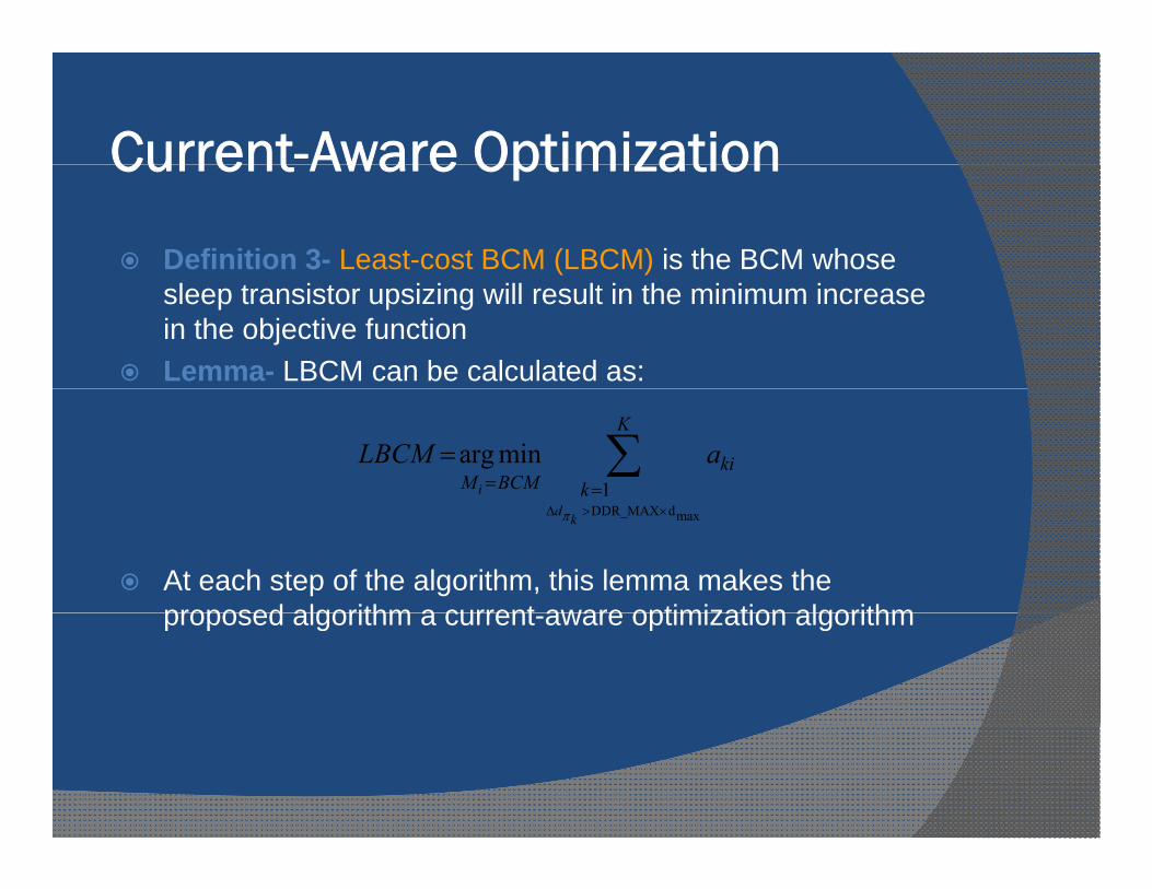
Definition 3- Least-cost BCM (LBCM) is the BCM whose sleep transistor upsizing will result in the minimum increase in the objective functionLemma- LBCM can be calculated as:
1
arg mini
K
kiM BCM k
LBCM a= =
= ∑
At each step of the algorithm, this lemma makes the proposed algorithm a current aware optimization algorithm
DDR_MAX dmaxd kπΔ > ×
proposed algorithm a current-aware optimization algorithm
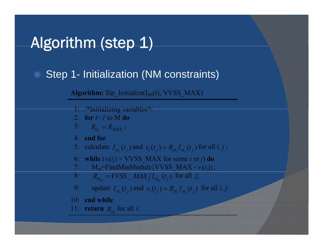
Algorithm (step 1)Algorithm (step 1)
Step 1- Initialization (NM constraints)Step 1 Initialization (NM constraints)Algorithm: Slp_Initialize(IMi(t), VVSS_MAX)
1: /*Initializing variables*/ 1: /*Initializing variables*/ 2: for i=1 to M do 3:
ist MAXR R= ;
4: end for 4: end for 5: calculate ( )
ist jI t and ( ) ( )i ii j st st jv t R I t= for all i, j ;
6: while (vi(tj) > VVSS_MAX for some i or j) do 7: Mm=FindMinModuleVVSS_MAX - vi(tj); 8: _ ( )
m mst st jR VVSS MAX I t= for all j;
9: update ( )ist jI t and ( ) ( )
i ii j st st jv t R I t= for all i, j;
10: end while11: return
istR for all i;
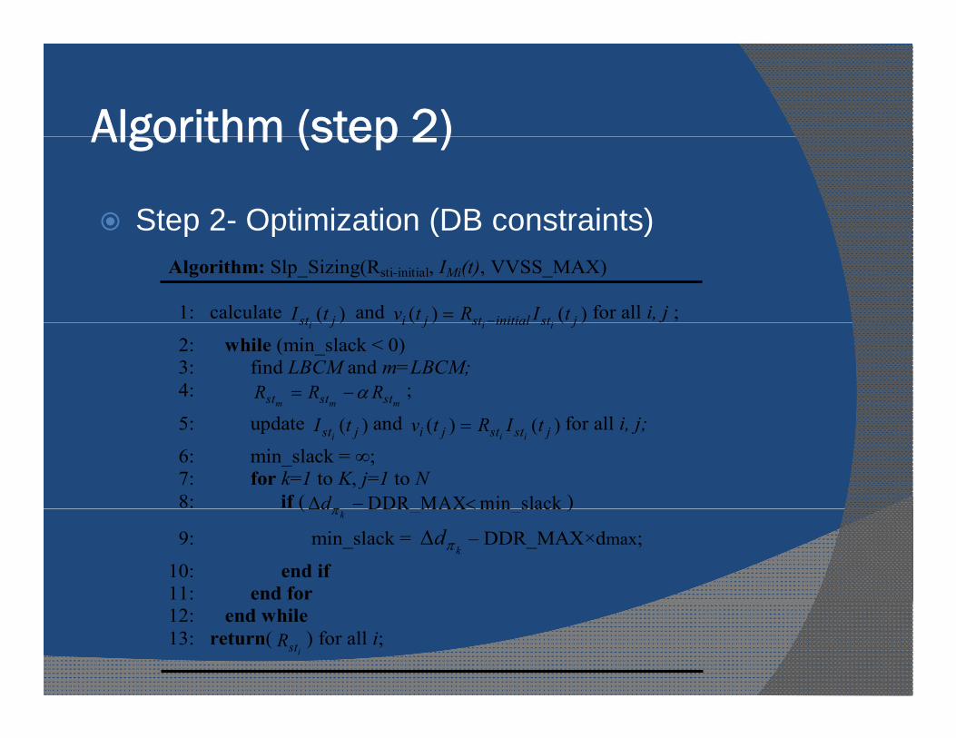
Algorithm (step 2)Algorithm (step 2)
Step 2- Optimization (DB constraints)Step 2 Optimization (DB constraints)Algorithm: Slp_Sizing(Rsti-initial, IMi(t), VVSS_MAX) 1: calculate ( )
ist jI t and ( ) ( )i ii j st initial st jv t R I t−= for all i, j ; ( )
ist j ( ) ( )i ii j st initial st j
2: while (min_slack < 0) 3: find LBCM and m=LBCM; 4:
m m mst st stR R Rα= − ;
5: update ( )ist jI t and ( ) ( )
i ii j st st jv t R I t= for all i, j;
6: min_slack = ∞; 7: for k=1 to K, j=1 to N 8: if ( DDR MAX min slackdπΔ − < ) ( DDR_MAX min_slack
kdπΔ < )
9: min_slack = k
dπΔ – DDR_MAX×dmax;
10: end if 11: end for12: end while 13: return(
istR ) for all i;

Simulation ApproachSimulation Approach
Max delay degradation ratio, DDR_MAX=10%Virtual rail resistance, Max number of the critical paths, K=100Resistance decrement factor α = 0 1
0.1iVSSr = Ω
Resistance decrement factor, α 0.1
Circuit # of cells # of Footers
Total sleep TX width (λ) Proposed vs. [X] (%)
Proposed vs. [Y] (%) [X]=[Chiou-
DAC’06][Y]=[Chiou-
DAC’07] Proposed DAC 06] DAC 07]C17 7 2 53 44 16 70 64
9sym 276 30 786 715 312 60 56 C432 214 30 811 665 343 57 48 C880 467 55 1290 1173 579 55 51
C1355 546 60 1437 1597 727 49 54 C3540 1307 280 3920 3469 1679 57 52 C5315 1783 320 5799 5631 3372 42 40 Avg. 2.0 1.89 1 55 52
ConclusionConclusion
A new sleep transistor sizing approach is proposedThe algorithm takes a max circuit slowdown factor andproduces the sizes of various sleep transistors while considering the DC parasitics of the virtual groundThe problem can be formulated as a sizing with delay-budgeting and solved efficiently using a heuristic sizingalgorithmalgorithmThe algorithm approaches the optimum solution by slowing down the modules with larger amount of discharging current more than the ones with smaller g gamount of discharging current, current-aware optimizationThe proposed technique uses at least 40% less total sleep transistor width compared to other approaches
Related Documents