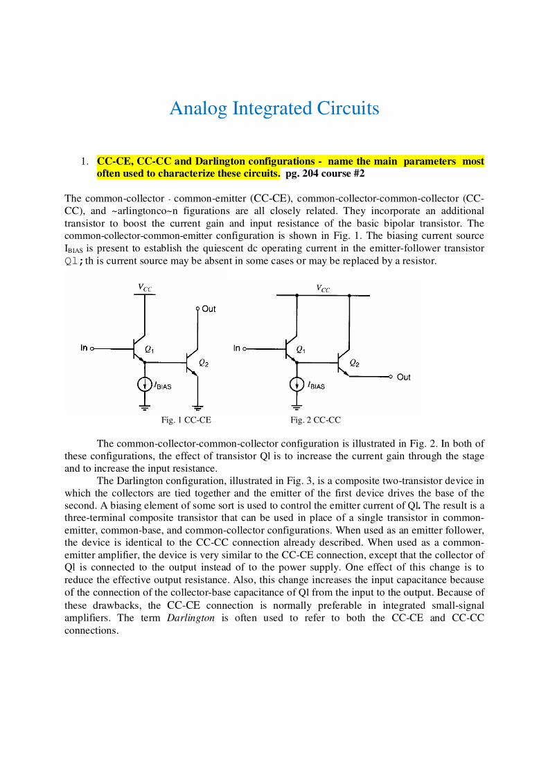
Analog Integrated Circuits 1. CC-CE, CC-CC and Darlington configurations - name the main parameters most often used to characterize these circuits. pg. 204 course #2 The common-collector - common-emitter (CC-CE), common-collector-common-collector (CC- CC), and ~arlingtonco~n figurations are all closely related. They incorporate an additional transistor to boost the current gain and input resistance of the basic bipolar transistor. The common-collector-common-emitter configuration is shown in Fig. 1. The biasing current source I BIAS is present to establish the quiescent dc operating current in the emitter-follower transistor Ql;th is current source may be absent in some cases or may be replaced by a resistor. Fig. 1 CC-CE Fig. 2 CC-CC The common-collector-common-collector configuration is illustrated in Fig. 2. In both of these configurations, the effect of transistor Ql is to increase the current gain through the stage and to increase the input resistance. The Darlington configuration, illustrated in Fig. 3, is a composite two-transistor device in which the collectors are tied together and the emitter of the first device drives the base of the second. A biasing element of some sort is used to control the emitter current of Ql . The result is a three-terminal composite transistor that can be used in place of a single transistor in common- emitter, common-base, and common-collector configurations. When used as an emitter follower, the device is identical to the CC-CC connection already described. When used as a common- emitter amplifier, the device is very similar to the CC-CE connection, except that the collector of Ql is connected to the output instead of to the power supply. One effect of this change is to reduce the effective output resistance. Also, this change increases the input capacitance because of the connection of the collector-base capacitance of Ql from the input to the output. Because of these drawbacks, the CC-CE connection is normally preferable in integrated small-signal amplifiers. The term Darlington is often used to refer to both the CC-CE and CC-CC connections.

Welcome message from author
This document is posted to help you gain knowledge. Please leave a comment to let me know what you think about it! Share it to your friends and learn new things together.
Transcript
Analog Integrated Circuits
1. CC-CE, CC-CC and Darlington configurations - name the main parameters most often used to characterize these circuits. pg. 204 course #2
The common-collector - common-emitter (CC-CE), common-collector-common-collector (CC-
CC), and ~arlingtonco~n figurations are all closely related. They incorporate an additional
transistor to boost the current gain and input resistance of the basic bipolar transistor. The
common-collector-common-emitter configuration is shown in Fig. 1. The biasing current source
IBIAS is present to establish the quiescent dc operating current in the emitter-follower transistor
Ql;th is current source may be absent in some cases or may be replaced by a resistor.
Fig. 1 CC-CE Fig. 2 CC-CC
The common-collector-common-collector configuration is illustrated in Fig. 2. In both of
these configurations, the effect of transistor Ql is to increase the current gain through the stage
and to increase the input resistance.
The Darlington configuration, illustrated in Fig. 3, is a composite two-transistor device in
which the collectors are tied together and the emitter of the first device drives the base of the
second. A biasing element of some sort is used to control the emitter current of Ql. The result is a
three-terminal composite transistor that can be used in place of a single transistor in common-
emitter, common-base, and common-collector configurations. When used as an emitter follower,
the device is identical to the CC-CC connection already described. When used as a common-
emitter amplifier, the device is very similar to the CC-CE connection, except that the collector of
Ql is connected to the output instead of to the power supply. One effect of this change is to
reduce the effective output resistance. Also, this change increases the input capacitance because
of the connection of the collector-base capacitance of Ql from the input to the output. Because of
these drawbacks, the CC-CE connection is normally preferable in integrated small-signal
amplifiers. The term Darlington is often used to refer to both the CC-CE and CC-CC
connections.

Fig. 3 Darlington configuration
2. The bipolar cascode configuration – draw the circuit, compare its output resistance with that of the common emitter stage. pg. 207, course #2
In bipolar form, the cascode is a common-emitter-common-base (CE-CB) amplifier, as
shown in Fig. 4.
Fig. 4 Bipolar cascode amplifier
Therefore, the CE-CB connection displays an output resistance that is larger by a factor of about
0β than the CE stage alone.

3. The dc transfer characteristic of an emitter-coupled pair - compare the schemes with and without emitter degeneration. pg. 215 – 217 (abstract), course #2.
Fig. 5 Emitter-coupled pair circuit diagram. Fig. 6 Emitter-coupled pair with emitter degeneration.
To increase the range of Vid over which the emitter-coupled pair behaves approximately as a
linear amplifier, emitter-degeneration resistors are frequently included in series with the emitters
of the transistors, as shown in Fig. 6. For large values of emitter-degeneration resistors, the
linear range of operation is extended by an amount approximately equal to TAIL EI R . This result
stems from the observation that all of TAILI flows in one of the degeneration resistors when one
transistor turns off. Therefore, the voltage drop is TAIL EI R on one resistor and zero on the other,
and the value of Vid required to turn one transistor off is changed by the difference of the voltage
drops on these resistors. The voltage gain is reduced by approximately the same factor that the
input range is increased. In operation, the emitter resistors introduce local negative feedback in
the differential pair.
4. Simple current mirror - bipolar version. Draw the schematic and compare it with an
ideal current mirror. pg. 256, course #4
Fig. 7 A simple bipolar current mirror.

A current mirror is an element with at least three terminals, as shown in Fig. 7. The common
terminal is connected to a power supply, and the input current source is connected to the input
terminal. Ideally, the output current is equal to the input current multiplied by a desired current
gain. If the gain is unity, the input current is reflected to the output, leading to the name current
mirror. Under ideal conditions, the current-mirror gain is independent of input frequency, and
the output current is independent of the voltage between the output and common terminals.
Furthermore, the voltage between the input and common terminals is ideally zero because this
condition allows the entire supply voltage to appear across the input current source, simplifying
its transistor-level design. In practice, real transistor-level current mirrors suffer many deviations
from this ideal behavior. For example, the gain of a real current mirror is never independent of
the input frequency. One of the most important deviations from ideality is the variation of the
current mirror output current with changes in voltage at the output terminal. This effect is
characterized by the small-signal output resistance, R,, of the current mirror. Another important
error source is the gain error, which is the deviation of the gain of a current mirror from its ideal
value.
5. Wilson current mirror – draw the schematic, estimate the value of the output
resistance and compare it with that of the cascode current mirror. pg. 277, Course
#6
Fig. 8 a) Bipolar Wilson current mirror. b Small signal model
This circuit uses negative feedback through Ql, activating Q3 to reduce the base-current error
and raise the output resistance.
If ∞→3or the small-signal current that flows in the collector of Q3 is equal to i1 and the output
resistance is
This result is the same as for the cascode current mirror.
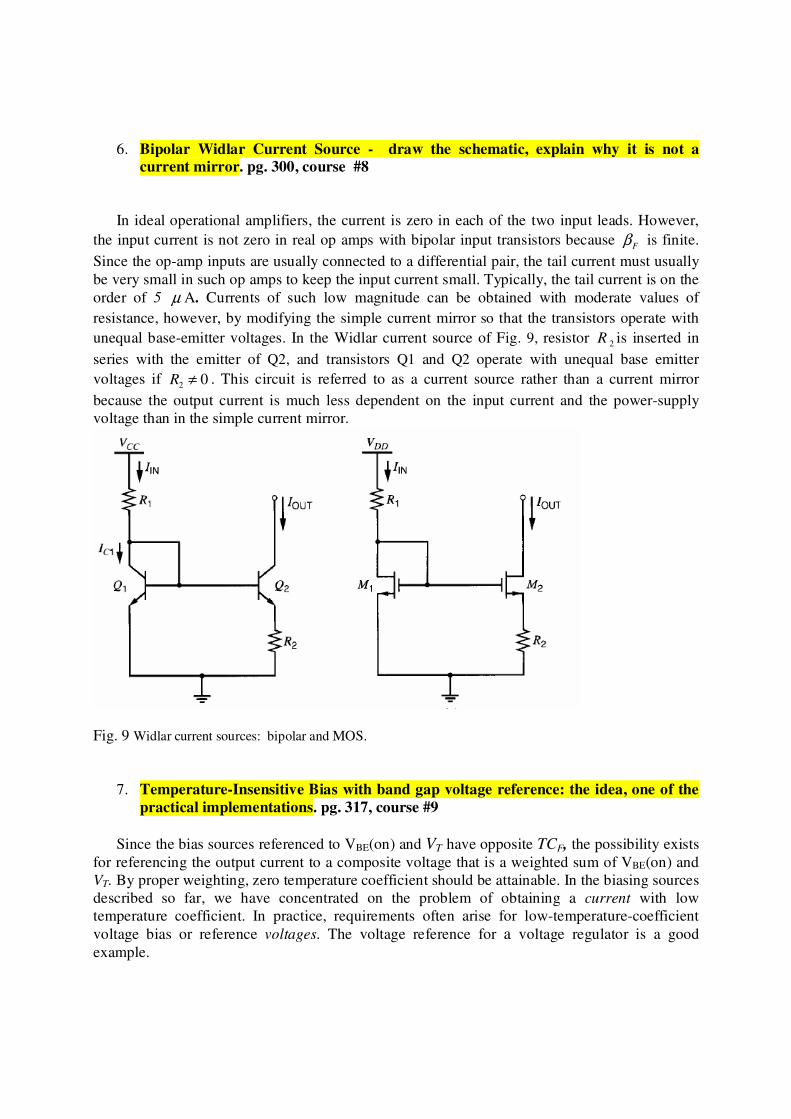
6. Bipolar Widlar Current Source - draw the schematic, explain why it is not a current mirror. pg. 300, course #8
In ideal operational amplifiers, the current is zero in each of the two input leads. However,
the input current is not zero in real op amps with bipolar input transistors because Fβ is finite.
Since the op-amp inputs are usually connected to a differential pair, the tail current must usually
be very small in such op amps to keep the input current small. Typically, the tail current is on the
order of 5 µ A. Currents of such low magnitude can be obtained with moderate values of
resistance, however, by modifying the simple current mirror so that the transistors operate with
unequal base-emitter voltages. In the Widlar current source of Fig. 9, resistor 2R is inserted in
series with the emitter of Q2, and transistors Q1 and Q2 operate with unequal base emitter
voltages if 2 0R ≠ . This circuit is referred to as a current source rather than a current mirror
because the output current is much less dependent on the input current and the power-supply
voltage than in the simple current mirror.
Fig. 9 Widlar current sources: bipolar and MOS.
7. Temperature-Insensitive Bias with band gap voltage reference: the idea, one of the
practical implementations. pg. 317, course #9
Since the bias sources referenced to VBE(on) and VT have opposite TCF, the possibility exists
for referencing the output current to a composite voltage that is a weighted sum of VBE(on) and
VT. By proper weighting, zero temperature coefficient should be attainable. In the biasing sources
described so far, we have concentrated on the problem of obtaining a current with low
temperature coefficient. In practice, requirements often arise for low-temperature-coefficient
voltage bias or reference voltages. The voltage reference for a voltage regulator is a good
example.

Fig. 10 Widlar band-gap reference.
A practical realization of band-gap reference, in bipolar technologies, takes the form illustrated
in Fig. 10. This circuit uses a feedback loop to establish an operating point in the circuit such that
the output voltage is equal to a VB plus a voltage proportional to the difference between two
base-emitter voltages.
8. Inverting and noninverting amplifier built with an op amp - draw the schematics
and find the gains, define the characteristics of an ideal op amp. pg. 406, 408, course
#9
Fig. 11 a) Inverting amplifier; b) Non-inverting amplifier
The inverting amplifier connection is shown in Fig. 11 a. We assume that the op-amp input
resistance is infinite, and that the output resistance is zero. From KCL at node X:
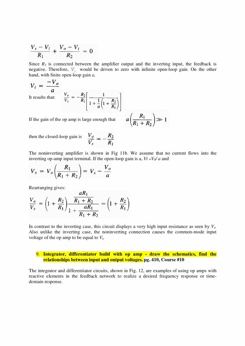
Since R2 is connected between the amplifier output and the inverting input, the feedback is
negative. Therefore, Vi would be driven to zero with infinite open-loop gain. On the other
hand, with finite open-loop gain a,
It results that:
If the gain of the op amp is large enough that
then the closed-loop gain is
The noninverting amplifier is shown in Fig 11b. We assume that no current flows into the
inverting op-amp input terminal. If the open-loop gain is a, Vi =V0/ a and
Rearranging gives:
In contrast to the inverting case, this circuit displays a very high input resistance as seen by Vs.
Also unlike the inverting case, the noninverting connection causes the common-mode input
voltage of the op amp to be equal to Vs.
9. Integrator, differentiator build with op amp - draw the schematics, find the
relationships between input and output voltages. pg. 410, Course #10
The integrator and differentiator circuits, shown in Fig. 12, are examples of using op amps with
reactive elements in the feedback network to realize a desired frequency response or time-
domain response.

Fig. 12 a) Integrator configuration b) Differentiator configuration
In the case of the integrator, the resistor R is used to develop a current I1 that is proportional to
the input voltage. This current flows into the capacitor C, whose voltage is proportional to the
integral of the current Il with respect to time. Since the output voltage is equal to the negative of
the capacitor voltage, the output is proportional to the integral of the input voltage with respect to
time. In terms of equations:
and
It results that:
In the case of the differentiator, the capacitor C is connected between Vs, and the inverting op-
amp input. The current through the capacitor is proportional to the time derivative of the voltage
across it, which is equal to the input voltage. This current flows through the feedback resistor R,
producing a voltage at the output proportional to the capacitor current, which is proportional to
the time rate of change of the input voltage. In terms of equations:
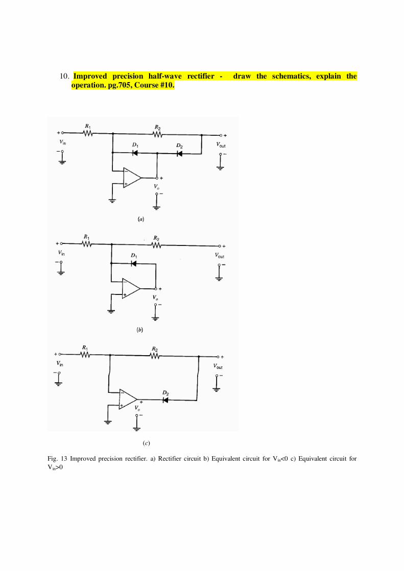
10. Improved precision half-wave rectifier - draw the schematics, explain the operation. pg.705, Course #10.
(c)
Fig. 13 Improved precision rectifier. a) Rectifier circuit b) Equivalent circuit for Vin<0 c) Equivalent circuit for
Vin>0

Diode D1 is forward biased and the op amp is in the active region. The inverting input of the op
amp is clamped at ground by the feedback through D1, and, since no current flows in R2, the
output voltage is also at ground. When the input voltage is made positive, no current can flow in
the reverse direction through D1 so the output voltage of the op amp Vo, is driven in the negative
direction. This reverse biases D1 and forward biases D
2. The resulting equivalent circuit is
shown in Fig. 13 c and is simply an inverting amplifier with a forward-biased diode in series
with the output lead of the op amp. Because of large gain of the op amp, this diode has no effect
on its behavior as long as it is forward biased, and so the circuit behaves as an inverting amplifier
giving an output voltage
Signal Processing
1- Where are the poles of a stable and causal analog system? Give an example.
http://shannon.etc.upt.ro/teaching/sp-pi/Course/1_Laplace.pdf slide 62
2- Define minimum phase analog systems. Give an example.
http://shannon.etc.upt.ro/teaching/sp-pi/Course/1_Laplace.pdf slide 63

3- Ideal low pass filter.
http://shannon.etc.upt.ro/teaching/sp-pi/Course/2_Filtering.pdf slide 6
4- Enunciate WKS sampling theorem.
http://shannon.etc.upt.ro/teaching/sp-pi/Course/3_Sampling.pdf slide 17

5- Spectrum of ideal sampled signal (Relation + Graphical representation).
http://shannon.etc.upt.ro/teaching/sp-pi/Course/3_Sampling.pdf slide 7,8

6- Approximation of continuous-time systems with discrete-time systems using impulse
invariance method.
http://shannon.etc.upt.ro/teaching/sp-pi/Course/5_Approximation.pdf slide 7
7- Approximation of RC circuit using bilinear transform method.
http://shannon.etc.upt.ro/teaching/sp-pi/Course/5_Approximation.pdf slide 38, 43

8- Demodulator (envelope detector) for AM signals.
http://shannon.etc.upt.ro/teaching/sp-pi/Course/6_Modulation.pdf slide 16

9- Narrow Band Frequency Modulation.
http://shannon.etc.upt.ro/teaching/sp-pi/Course/6_Modulation.pdf slide 49
10- Nyquist stability criterion for continuous-time systems when the open loop system is stable
(schema + enunciation).
http://shannon.etc.upt.ro/teaching/sp-pi/Course/7_Stability.pdf slide 22(schema), 37 (enunciation)

Electronic Instrumentation
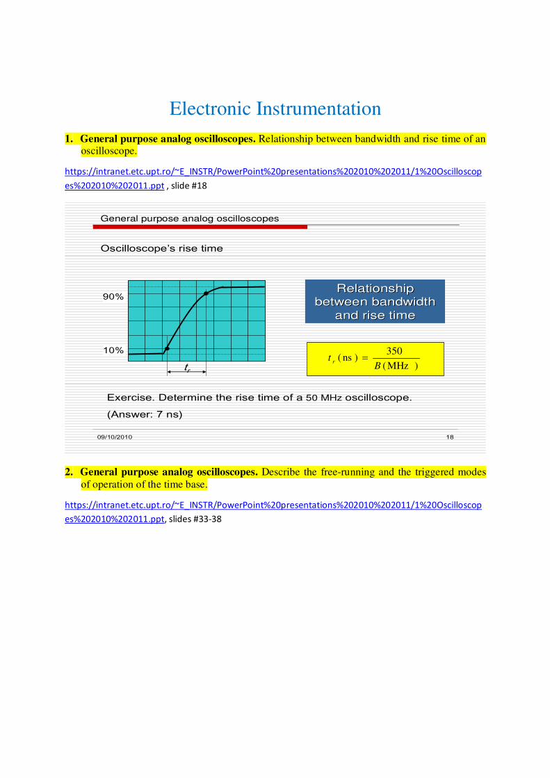
1. General purpose analog oscilloscopes. Relationship between bandwidth and rise time of an oscilloscope.
https://intranet.etc.upt.ro/~E_INSTR/PowerPoint%20presentations%202010%202011/1%20Oscilloscop
es%202010%202011.ppt , slide #18
09/10/2010 18
Oscilloscope’s rise time
General purpose analog oscilloscopes
tr
10%
90%
)MHz(
350)ns(
Bt r =
Relationship Relationship
between bandwidth between bandwidth
and rise timeand rise time
Exercise. Determine the rise time of a 50 MHz oscilloscope.
(Answer: 7 ns)
2. General purpose analog oscilloscopes. Describe the free-running and the triggered modes
of operation of the time base.
https://intranet.etc.upt.ro/~E_INSTR/PowerPoint%20presentations%202010%202011/1%20Oscilloscop
es%202010%202011.ppt, slides #33-38

09/10/2010 33
Sweep generator – two operating modes: free-running and triggered
General purpose analog oscilloscopes
0 td ti
TBT
uBT
t
ud
0 td ti
TBT
uBT
tta
t
Direct sweep
Re-armHold-off time
With triggered sweeps, the scope will blank the beam and start to reset the sweep circuit (re-arm)
each time the beam reaches the extreme right side of the screen. For a period of time, called
hold-off, the sweep circuit resets completely and ignores triggers. Once hold-off expires, the next
trigger starts a sweep. The trigger event is usually the input waveform reaching some user-
specified threshold voltage (trigger level) in the specified direction (going positive or going
negative - trigger polarity). Triggering circuit ensures a stable image on the screen.
Triggering condition YBT kTT =
The sweep generator’s period should be a multiple of the signal period. Timing diagrams
(triggered sweep):
t
t
t
0
0
0
A un uY un
ud
uBT
TY TBT
3. Probes for oscilloscopes. Attenuating probes. Frequency compensation. Describe what
happens and tell (and draw) how the image of square pulses appears on the screen when the compensation condition is not met.
https://intranet.etc.upt.ro/~E_INSTR/PowerPoint%20presentations%202010%202011/1%20Oscilloscop
es%202010%202011.ppt, slides #23-25
09/10/2010 23
Passive probe with attenuator (in the probe head)
General purpose analog oscilloscopes
ini RRR +=ccinc
ccinc
iCCC
CCCC
++
+⋅=
)(
R
uY
Cc
Rin Cin
Coaxial cable
OSCILLOSCOPEProbe head
Ccc
Oscilloscope
mode
AUTO
NORMAL
sweep generator – free running with no
trigger
sweep generator – triggered by the trigger
signal
sweep generator – in standby with no
trigger
sweep generator – triggered by the trigger
signal
Probes without and with attenuator - comparison
Probe without attenuator
advantage – it does not attenuate the input signal
disadvantage – relatively small input resistance (1 MΩ), large input capacitance (50 - 150
pF)
Probe with attenuator
advantage – large input resistance (10 MΩ), small input capacitance (5 - 15 pF)
disadvantage – it attenuates the input signal (therefore, the value read on the display
must be multiplied by the probe’s attenuation factor)
4. General purpose analog oscilloscopes. Delayed sweep: use, operating modes, utility.
https://intranet.etc.upt.ro/~E_INSTR/PowerPoint%20presentations%202010%202011/1%20Oscilloscop
es%202010%202011.ppt, slides #48-50
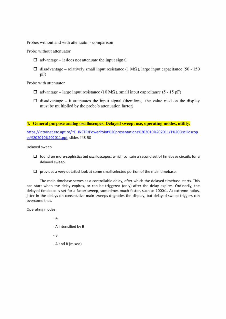
Delayed sweep
found on more-sophisticated oscilloscopes, which contain a second set of timebase circuits for a
delayed sweep.
provides a very-detailed look at some small selected portion of the main timebase.
The main timebase serves as a controllable delay, after which the delayed timebase starts. This
can start when the delay expires, or can be triggered (only) after the delay expires. Ordinarily, the
delayed timebase is set for a faster sweep, sometimes much faster, such as 1000:1. At extreme ratios,
jitter in the delays on consecutive main sweeps degrades the display, but delayed-sweep triggers can
overcome that.
Operating modes
- A
- A intensified by B
- B
- A and B (mixed)

09/10/2010 50
Delayed sweep – modes of operation
General purpose analog oscilloscopes
A A intensified by B B A and B
Timebase A
Timebase B
1 µs/div 1 µs/div 1 µs/div
100 ns/div 100 ns/div 100 ns/div
5. Signal generators. Describe the operation of the pulse generator in single and double pulses
modes.
https://intranet.etc.upt.ro/~E_INSTR/PowerPoint%20presentations%202010%202011/2%20Signal%20G
enerators%202010%202011.ppt, slides #8-11
21/01/2011 8
Block diagram of an impulse generator
Impulse generators
Trigger block
Delay shaper
Trigger impulse shaping
Frequency
Internal/External
Normal/Gated
Delay
AAAA BBBBKKKK1111
Width shaper
Width
Rise and fall time
adjustment
Output stage
Amplitude +
ud
K2 IDIS
Output stage
tr tf
Amplitude -
ue+
ue-
uesuis up

Operating modes
1. NORMAL
internally triggered (simple or double impulses)
externally triggered (simple or double impulses)
single impulses (simple or double impulses)
2. GATED
simple or double impulses
Operating modes
Normal, internally triggered, simple positive impulses
The trigger block operates autonomously and sets the repetition rate of the generated impulses.
The generator provides, in each cycle, a trigger pulse and one pulse at each output (positive and
negative), delayed with respect to the trigger pulse.
21/01/2011 11
Operating modesNormal, internally (or externally) triggered, simple or double
positive impulses
Impulse generators
ues
Period
Width
Delay
Amplitude
t
t
t
ue+
ue+

6. Signal generators. Describe the operation principle of a Direct Digital Synthesis generator.
https://intranet.etc.upt.ro/~E_INSTR/PowerPoint%20presentations%202010%202011/2%20Signal%20G
enerators%202010%202011.ppt, slides #35-36
21/01/2011 35
Direct digital synthesis generators
Oscillator (clock generator) – frequency f0Counter – n bits (0 - 2n-1) = memory addressStored values: sin(2πi/2n)Output frequency: f0/2n
Sine wave generators
OSCILLATOR COUNTER MEMORY DAC Uout
21/01/2011 36
Direct digital synthesis generators - example (n=4)
Sine wave generators

7. Digital voltmeters and multimeters. Error and data presentation rules.
https://intranet.etc.upt.ro/~E_INSTR/PowerPoint%20presentations%202010%202011/3%20Digital%20V
oltmeters%20and%20Multimeters%202010%202011.ppt, slides #7-10
21/01/2011 7
The maximum permissible error
∆t=a% × reading + b% × range + n digits
∆t=a% × reading + c% × range
∆t=a% × reading + m digits
Remark. One digit represents one LSD.
Example. One digit is 1 mV in case of a 2 V, 31/2 digit DVM(readout x,xxx V).
Introduction
21/01/2011 8
Introduction
Data presentation rules
1. Measurement error and uncertainty should be expressed with no more than two significant digits.
2. The LSD of the measurement result and of its corresponding error/uncertainty should have the same weight.
Examples.
0,0222 mA0,02 mA
3,58 mV3,5 mV
0,256%0,2%
WrongRight
1,53 V ± 3 mV1,538 V ± 3 mV
1,538 V ± 0,03 V1,538 V ± 0,003 V
1 ± 0,2 mA1,0 ± 0,2 mA
WrongRight

8. Digital voltmeters and multimeters. Define normal and common mode voltages and the respective rejection ratios (NMRR and CMRR)
https://intranet.etc.upt.ro/~E_INSTR/PowerPoint%20presentations%202010%202011/3%20Digital%20V
oltmeters%20and%20Multimeters%202010%202011.ppt, slides #20, 23, 28
21/01/2011 20
Measurement errors due to external noise
DC digital voltmeters
VoltmeterUx
Us
VoltmeterUx
Ucm
Normal mode voltage(DC or AC)
Common mode voltage(DC or AC)
21/01/2011 23
The ability of a DC DVM to reject an AC normal mode signal is described by the Normal Mode Rejection Ratio (acronym NMRR):
voltageDC equivalent
voltagemode normal theof amplitude=NMRR
DC digital voltmeters
Example. For a DC DVM with a NMRR of 100, a normal mode voltage with an amplitude of 1 V produces an additional error of
1 V/100 = 0,01 V = 10 mV.
21/01/2011 28
The ability of a DC DVM to reject a common mode signal is described by Common Mode Rejection Ratio (acronym CMRR):
ăechivalent serie tensiunea
comun mod de areperturbato tensiunea=CMRR
DC digital voltmeters
Aplicaţie. Un voltmetru de tensiune continuă are CMRR = 1000. O tensiune de mod comun de 5 V conduce la o tensiune serie echivalentă de 5 V/1000 = 5 mV.
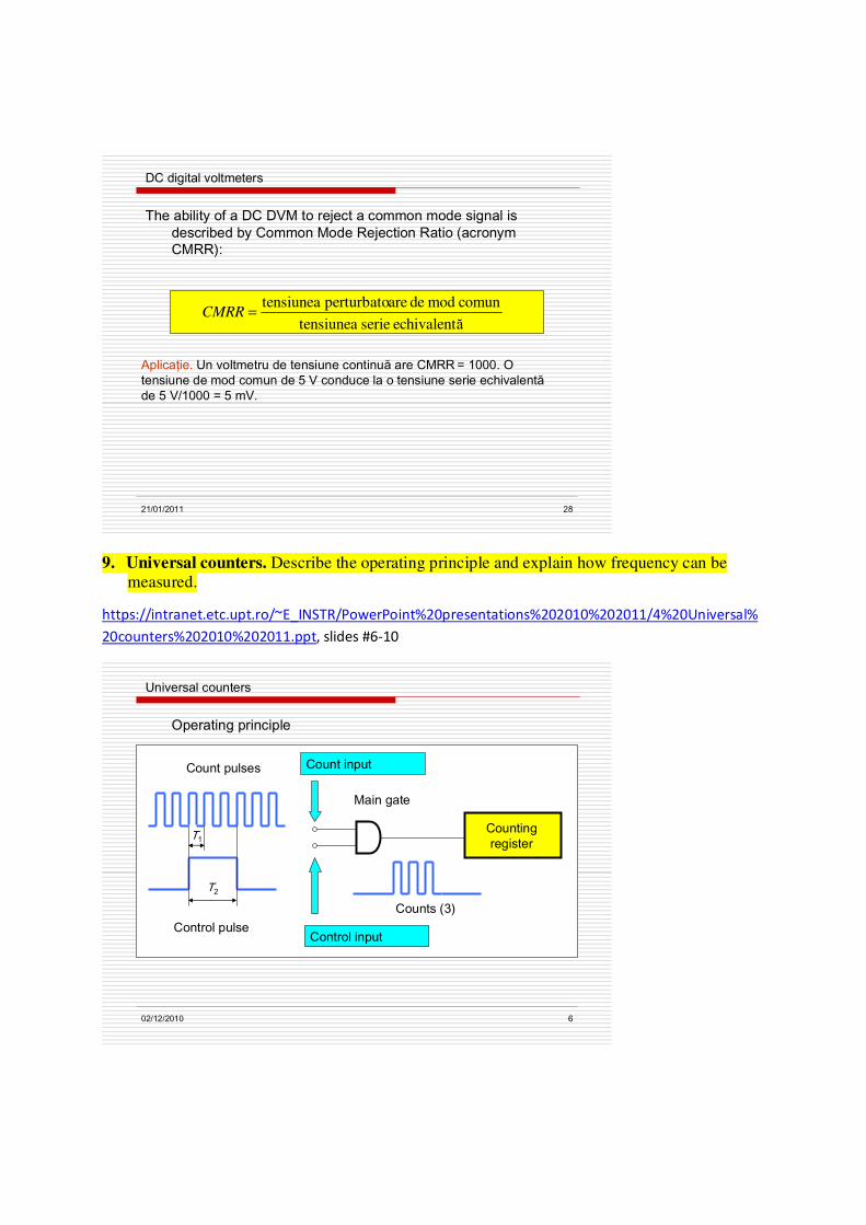
9. Universal counters. Describe the operating principle and explain how frequency can be
measured.
https://intranet.etc.upt.ro/~E_INSTR/PowerPoint%20presentations%202010%202011/4%20Universal%
20counters%202010%202011.ppt, slides #6-10
02/12/2010 6
Operating principle
Universal counters
Counting register
Count pulses
Control pulse
Main gate
Counts (3)
T1
T2
Count input
Control input

Displayed result:
or
Frequency measurement
The frequency f of a repetitive signal can be defined by the number of cycles of that signal per
unit of time
f=n/t,
where n is the number of cycles and t is the time interval in which they occur. As suggested by
the above equation, the frequency can be measured by counting the number of cycles and
dividing it by t. By taking t equal to one second, the number of counted cycles will represent the
frequency (in Hz) of the signal.
The input signal is initially conditioned to a form that is compatible with the internal circuitry of
the counter. The conditioned signal is a pulse train where each pulse corresponds to a cycle of
the input signal. With the main gate open, pulses are allowed to pass through and get totalized by
the counting register.
02/12/2010 10
Basic block diagram of a universal counter in the frequency measurement mode
The time base oscillator together with the decade dividers and the main gate flip flop control the opening time of the main gate.
Universal counters
1
2
T
TN x =
21TfN x =

10. Universal counters. Trigger error for period measurements.
https://intranet.etc.upt.ro/~E_INSTR/PowerPoint%20presentations%202010%202011/4%20Universal%
20counters%202010%202011.ppt, slides #24-26
02/12/2010 24
Period measurement – trigger error
Errors of universal counters
Tx
Threshold
0 t
ux
Δt
BA
02/12/2010 25
Trigger error
for single period measurement
for multiple period averaging
Errors of universal counters
ZSb
/
1
⋅=
πδ
S/Z = signal to noise ratio
ZSNb
/
1
⋅⋅=
πδ

02/12/2010 26
Measurement uncertainty
frequency meaurement
period measurement
osccfx δ+δ=δ lim
bosccTx δ+δ+δ=δ lim
Errors of universal counters
Related Documents