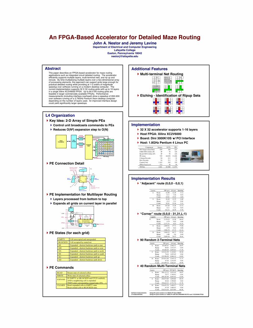
L4 Organization } Key Idea: 2-D Array of Simple PEs } Control unit broadcasts commands to PEs } Reduces O(N 2 ) expansion step to O(N) } PE Connection Detail } PE Implementation for Multilayer Routing } Layers processed from bottom to top } Expands all grids on current layer in parallel } PE States (for each grid) } PE Commands An FPGA-Based Accelerator for Detailed Maze Routing John A. Nestor and Jeremy Lavine Department of Electrical and Computer Engineering Lafayette College Easton, Pennsylvania 18042 [email protected] Abstract This paper describes an FPGA-based accelerator for maze routing applications such as integrated circuit detailed routing. The accelerator efficiently supports multiple layers, multi-terminal nets, and rip up and reroute. By time-multiplexing multiple layers over a two-dimensional array of processing elements, this approach can support grids large enough for practical detailed routing while providing at 1-2 orders of magnitude speedup over software running on a modern desktop computer. The current implementation supports 32 X 32 routing grids with up to 16 layers in a single Xilinx XC2V6000 FPGA. Up to 64 X 64 routing grids are feasible in larger commercially available FPGAs. Performance measurements (including interface overhead) show a speedup of 29X-93X over software running on a 3.79GHz Pentium Xeon desktop computer depending on the number of layers used. An improved interface design could yield significantly larger speedups. Implementation } 32 X 32 accelerator supports 1-16 layers } Host FPGA: Xilinx XC2V6000 } Board: Dini 3000K10S w/ PCI Interface } Host: 1.8GHz Pentium 4 Linux PC Implementation Results } “Adjacent” route (0,0,0 - 0,0,1) } “Corner” route (0,0,0 - 31,31,L-1) } 90 Random 2-Terminal Nets } 40 Random Multi-Terminal Nets Additional Features } Multi-terminal Net Routing } Etching - Identification of Ripup Sets Column Dec. R o w D e c. Control Unit PE status out PE command, status in PCI Target routing commands routing results rs1 rs2 cs1 cs2 PE Array FIFO FIFO Host Computer EI WI NI SI XO XO XO XO SI XO WI XO NI XO EI XO SEL CMD STO 3 2 North Neighbor South Neighbor RSEL CSEL East Neighbor West Neighbor CMD STATE OUT clk PREF pref STI STATE IN Broadcast to all PEs from Control Unit Logical AND of PE outputs to Control Unit 3 D Q XL XH /TOP CLK SEQUENCER ST0 SREG NS CS HI LI NI SI EI WI RSEL CSEL CMD ST to adjacent cells from decoders CMD STATUS PFV EN 1 0 PF PFEW PFNS EN XO D Q ETCH ETCH T1 T3 T2 T1 T3 T2 T1 T2 T1 T3 T2 T3 T1 T3 T2 T1 T3 T2 (a) (b) (c) (f) (e) (d) S1 T1 T2 (a) (b) (c) (f) (e) S2 T2 S2 S1 T1 T2 S2 S1 T1 S2 S1 T1 T2 S2 S1 T1 S1 T1 T2 S2 (d) T2 EMPTY Cell unoccupied and unexpanded BLOCKED Cell occupied by routed net XE Expanded - shortest backtrace path to east XW Expanded - shortest backtrace path to west XN Expanded - shortest backtrace path to north XS Expanded - shortest backtrace path to south XU Expanded - shortest backtrace path up XD Expanded - shortest backtrace path down READ Return state of selected cell(s) WRITE Write state of selected cell(s) EXPAND IF EMPTY or (BLOCKED and ETCH enabled), AND a neighboring cell is expanded THEN enter corresponding expand state (XN, …) CLEARX Reset expanded cells to EMPTY state Reset etched cells to BLOCKED state Component Source LUTs FFs PCI Target (from Dini) 529 164 223 CMD FIFO (Xilinx IP) IP 78 126 Result FIFO (Xilinx IP) IP 78 126 PE Array 749 64,838 11,268 Column Decoder 94 211 32 Row Decoder 94 211 32 Control Unit 1,103 362 129 FPGA Top Level 272 38 39 TOTAL 2,841 65,980 11,975 Layers SW (μs) L4 (μs) Speedup 6 Route 85,585.41 2,964.37 28.87 Ripup 80.64 1,931.47 0.04 Comb. 85,666.05 4,895.84 17.49 8 Route 119,321.59 3,110.83 38.36 Ripup 74.62 1,853.49 0.04 Comb. 119,396.20 4,964.32 24.05 16 Route 253,031.40 3,545.12 71.37 Ripup 67.95 1,516.95 0.04 Comb. 253,099.35 5,062.07 49.99 Layers SW (μs) L4 (μs) Speedup 6 Route 108,112.72 2,932.49 36.87 Ripup 70.77 1,760.93 0.04 Comb. 108,183.49 4,693.42 23.05 8 Route 150,573.09 3,050.88 49.35 Ripup 69.44 1,700.88 0.04 Comb. 150,642.53 4,751.76 31.70 16 Route 324,452.70 3,468.57 93.54 Ripup 61.58 1,406.43 0.04 Comb. 324,514.28 4,875.00 66.56 Software measurements: Using P4 cycle counter on 3.79GHz P4 Xeon EM64T L4 measurements: Using P4 cycle counter on 1.8GHz P4 with Dini DN3000K10S PCI card / XC2V6000 FPGA Layers SW (μs) L4 (μs) Speedup 6 Route 62.90 12.29 5.12 Ripup 0.11 3.26 0.03 Comb. 63.01 15.55 4.05 8 Route 82.49 12.35 6.68 Ripup 0.12 3.21 0.04 Comb. 82.61 15.56 5.31 16 Route 162.20 13.38 12.12 Ripup 0.11 3.21 0.03 Comb. 162.31 16.59 9.78 Layers SW (μs) L4 (μs) Speedup 6 Route 2,170.52 32.58 66.62 Ripup 0.79 9.82 0.08 Comb. 2,171.31 42.4 51.21 8 Route 2,905.91 37.71 77.06 Ripup 0.79 9.62 0.08 Comb. 2,906.70 47.33 61.41 16 Route 5,849.52 66.77 87.61 Ripup 0.86 9.8 0.09 Comb. 5,850.38 76.57 76.41

Welcome message from author
This document is posted to help you gain knowledge. Please leave a comment to let me know what you think about it! Share it to your friends and learn new things together.
Transcript
L4 Organization} Key Idea: 2-D Array of Simple PEs} Control unit broadcasts commands to PEs} Reduces O(N2) expansion step to O(N)
} PE Connection Detail
} PE Implementation for Multilayer Routing} Layers processed from bottom to top} Expands all grids on current layer in parallel
} PE States (for each grid)
} PE Commands
An FPGA-Based Accelerator for Detailed Maze RoutingJohn A. Nestor and Jeremy LavineDepartment of Electrical and Computer Engineering
Lafayette CollegeEaston, Pennsylvania 18042
AbstractThis paper describes an FPGA-based accelerator for maze routingapplications such as integrated circuit detailed routing. The acceleratorefficiently supports multiple layers, multi-terminal nets, and rip up andreroute. By time-multiplexing multiple layers over a two-dimensional arrayof processing elements, this approach can support grids large enough forpractical detailed routing while providing at 1-2 orders of magnitudespeedup over software running on a modern desktop computer. Thecurrent implementation supports 32 X 32 routing grids with up to 16 layersin a single Xilinx XC2V6000 FPGA. Up to 64 X 64 routing grids arefeasible in larger commercially available FPGAs. Performancemeasurements (including interface overhead) show a speedup of 29X-93Xover software running on a 3.79GHz Pentium Xeon desktop computerdepending on the number of layers used. An improved interface designcould yield significantly larger speedups.
Implementation} 32 X 32 accelerator supports 1-16 layers} Host FPGA: Xilinx XC2V6000} Board: Dini 3000K10S w/ PCI Interface} Host: 1.8GHz Pentium 4 Linux PC
Implementation Results} “Adjacent” route (0,0,0 - 0,0,1)
} “Corner” route (0,0,0 - 31,31,L-1)
} 90 Random 2-Terminal Nets
} 40 Random Multi-Terminal Nets
Additional Features} Multi-terminal Net Routing
} Etching - Identification of Ripup Sets
Column Dec.
Row Dec.
ControlUnit
PE status out
PE command,status in
PCITarget
routing commands
routingresults
rs1
rs2
cs1 cs2
PE Array
FIFO
FIFO
HostComputer
EI WI
NI
SI
XO
XO
XO
XO SI
XO
WI XO
NI XO
EI XO
SEL CMD
STO 3
2
North Neighbor
South Neighbor
RSEL
CSEL
EastNeighbor
WestNeighbor
CMD
STATE OUTclk
PREF
pref
STI
STATE IN
Broadcast to all PEsfrom Control Unit
Logical AND of PE outputsto Control Unit
3
D QXL
XH/TOP
CLK
SEQUENCERST0
SREG
NSCSHI
LI NI SI EI WI
RSEL CSEL CMD
ST
to adjacent cells
fromdecoders CMD
STATUS
PFV
EN
1 0
PF
PFEWPFNS
EN
XO
D Q
ETCHETCH
T1
T3
T21
1 2
2
2
3
3
3
3
4
4
4
T1
T3
T2
T1T2
T1
T3
T21 1 1
1111
2 2 2 2T3
T1
T3
T2
T1
T3
T2
(a) (b) (c)
(f)(e)(d)
1S1
T1
T2
(a) (b) (c)
(f)(e)
S21
2
1
T2S21
2
S1
T1
3
3
1
T2S21
2
S1
T1
3
3
4
1
S21
2
S1
T1
3
3 4
T2S2S1
T1
S1
T1
T2S2
(d)
4T2
EMPTY Cell unoccupied and unexpandedBLOCKED Cell occupied by routed netXE Expanded - shortest backtrace path to east XW Expanded - shortest backtrace path to west XN Expanded - shortest backtrace path to north XS Expanded - shortest backtrace path to south XU Expanded - shortest backtrace path up XD Expanded - shortest backtrace path down
READ Return state of selected cell(s)WRITE Write state of selected cell(s)
EXPAND
IF EMPTY or (BLOCKED and ETCH enabled)!, AND a neighboring cell is expandedTHEN enter corresponding expand state (XN, …)
CLEARX
Reset expanded cells to EMPTY state Reset etched cells to BLOCKED state
Component Source LUTs FFsPCI Target (from Dini) 529 164 223CMD FIFO (Xilinx IP) IP 78 126Result FIFO (Xilinx IP) IP 78 126PE Array 749 64,838 11,268Column Decoder 94 211 32Row Decoder 94 211 32Control Unit 1,103 362 129FPGA Top Level 272 38 39TOTAL 2,841 65,980 11,975
Layers SW (µs) L4 (µs) Speedup6 Route 85,585.41 2,964.37 28.87
Ripup 80.64 1,931.47 0.04Comb. 85,666.05 4,895.84 17.49
8 Route 119,321.59 3,110.83 38.36Ripup 74.62 1,853.49 0.04Comb. 119,396.20 4,964.32 24.05
16 Route 253,031.40 3,545.12 71.37Ripup 67.95 1,516.95 0.04Comb. 253,099.35 5,062.07 49.99
Layers SW (µs) L4 (µs) Speedup6 Route 108,112.72 2,932.49 36.87
Ripup 70.77 1,760.93 0.04Comb. 108,183.49 4,693.42 23.05
8 Route 150,573.09 3,050.88 49.35Ripup 69.44 1,700.88 0.04Comb. 150,642.53 4,751.76 31.70
16 Route 324,452.70 3,468.57 93.54Ripup 61.58 1,406.43 0.04Comb. 324,514.28 4,875.00 66.56
Software measurements: Using P4 cycle counter on 3.79GHz P4 Xeon EM64TL4 measurements: Using P4 cycle counter on 1.8GHz P4 with Dini DN3000K10S PCI card / XC2V6000 FPGA
Layers SW (µs) L4 (µs) Speedup6 Route 62.90 12.29 5.12
Ripup 0.11 3.26 0.03Comb. 63.01 15.55 4.05
8 Route 82.49 12.35 6.68Ripup 0.12 3.21 0.04Comb. 82.61 15.56 5.31
16 Route 162.20 13.38 12.12Ripup 0.11 3.21 0.03Comb. 162.31 16.59 9.78
Layers SW (µs) L4 (µs) Speedup6 Route 2,170.52 32.58 66.62
Ripup 0.79 9.82 0.08Comb. 2,171.31 42.4 51.21
8 Route 2,905.91 37.71 77.06Ripup 0.79 9.62 0.08Comb. 2,906.70 47.33 61.41
16 Route 5,849.52 66.77 87.61Ripup 0.86 9.8 0.09Comb. 5,850.38 76.57 76.41
Related Documents