Sensors & Transducers, Vol. 157, Issue 10, October 2013, pp. 190-197 190 S S S e e e n n n s s s o o o r r r s s s & & & T T T r r r a a a n n n s s s d d d u u u c c c e e e r r r s s s © 2013 by IFSA http://www.sensorsportal.com A Low Voltage Delta-Sigma Fractional Frequency Divider for Multi-band WSN Frequency Synthesizers 1 Fan Xiangning, 2 Yuan Liang 1, 2 Institute of RF-&OE-ICs, School of Information Science and Engineering, Southeast University, Nanjing, 210096, China 2 E-mail: [email protected] Received: 29 July 2013 /Accepted: 25 October 2013 /Published: 31 October 2013 Abstract: A 1 V low voltage delta-sigma fractional-N frequency divider for multi-band (780/868/915 MHz and 2.4 GHz) WSN frequency synthesizers is presented. The frequency divider consists of a dual-modulus prescaler, a pulse-swallow counter and a delta-sigma modulator. The high-speed and low-voltage phase-switching dual- modulus prescaler is used in the frequency divider. Low threshold voltage transistors are applied to overcome low voltage supply and forward phase-switching technique is adopted to prevent glitches. The modified delta- sigma modulator with long output sequence length and less spurs is adopted to minimize the fractional spurs. The frequency divider is designed in 0.18 μm TSMC RF CMOS technology under 1 V supply instead of the standard 1.8 V supply. The total chip area is 1190 μm × 485 μm including I/O pads. The post simulation results show the frequency divider operates normally over a wide range of 1.3-5.0 GHz and the core circuit (without test buffers) consumes 2.3 mW. Copyright © 2013 IFSA. Keywords: Low voltage, Fractional frequency divider, Delta-sigma modulator, Phase-switching prescaler, Wireless sensor networks. 1. Introduction Wireless sensor networks (WSN) have attracted increasing attention and interest in wireless communication. ZigBee (IEEE 802.15.4) has been introduced into WSN because of low-cost, low power consumption, extended battery life, flexibility and autonomy. In WSN transceiver system, the frequency synthesizer based on phase-locked loop (PLL) structure generates the local oscillator signals for the transmitter and receiver [1, 2]. In the frequency synthesizer design, the frequency divider is the mixed signal block combining the analog and digital circuits [3]. Special consideration is needed when designing the low voltage and high-speed prescaler in the frequency divider because the prescaler works at the low supply voltage 1 V and the highest frequency of 5 GHz. As the load of voltage- controlled oscillator, the frequency divider should have small input capacitance. This paper presents the fractional-N frequency divider for dual-band ZigBee frequency synthesizers. In this paper, 1 V low voltage power supply is used instead of the typical 1.8 V for the standard 0.18 μm TSMC RF CMOS technology. The paper is organized as follows. The architecture of the frequency synthesizer and the frequency divider are illustrated in Section 2. The circuit design is given in Section 3. Section 4 presents the layout design and post simulation results. The conclusion is shown in Section 5. 2. Architecture of Frequency Synthesizers The architecture of the frequency synthesizer and the fractional-N frequency divider are illustrated in Fig. 1. The frequency synthesizer consists of voltage- Article number P_1411

Welcome message from author
This document is posted to help you gain knowledge. Please leave a comment to let me know what you think about it! Share it to your friends and learn new things together.
Transcript

Sensors & Transducers, Vol. 157, Issue 10, October 2013, pp. 190-197
190
SSSeeennnsssooorrrsss &&& TTTrrraaannnsssddduuuccceeerrrsss
© 2013 by IFSAhttp://www.sensorsportal.com
A Low Voltage Delta-Sigma Fractional Frequency Divider for Multi-band WSN Frequency Synthesizers
1 Fan Xiangning, 2 Yuan Liang
1, 2 Institute of RF-&OE-ICs, School of Information Science and Engineering, Southeast University, Nanjing, 210096, China
2 E-mail: [email protected]
Received: 29 July 2013 /Accepted: 25 October 2013 /Published: 31 October 2013 Abstract: A 1 V low voltage delta-sigma fractional-N frequency divider for multi-band (780/868/915 MHz and 2.4 GHz) WSN frequency synthesizers is presented. The frequency divider consists of a dual-modulus prescaler, a pulse-swallow counter and a delta-sigma modulator. The high-speed and low-voltage phase-switching dual-modulus prescaler is used in the frequency divider. Low threshold voltage transistors are applied to overcome low voltage supply and forward phase-switching technique is adopted to prevent glitches. The modified delta-sigma modulator with long output sequence length and less spurs is adopted to minimize the fractional spurs. The frequency divider is designed in 0.18 µm TSMC RF CMOS technology under 1 V supply instead of the standard 1.8 V supply. The total chip area is 1190 µm × 485 µm including I/O pads. The post simulation results show the frequency divider operates normally over a wide range of 1.3-5.0 GHz and the core circuit (without test buffers) consumes 2.3 mW. Copyright © 2013 IFSA. Keywords: Low voltage, Fractional frequency divider, Delta-sigma modulator, Phase-switching prescaler, Wireless sensor networks. 1. Introduction
Wireless sensor networks (WSN) have attracted
increasing attention and interest in wireless communication. ZigBee (IEEE 802.15.4) has been introduced into WSN because of low-cost, low power consumption, extended battery life, flexibility and autonomy. In WSN transceiver system, the frequency synthesizer based on phase-locked loop (PLL) structure generates the local oscillator signals for the transmitter and receiver [1, 2]. In the frequency synthesizer design, the frequency divider is the mixed signal block combining the analog and digital circuits [3]. Special consideration is needed when designing the low voltage and high-speed prescaler in the frequency divider because the prescaler works at the low supply voltage 1 V and the highest frequency of 5 GHz. As the load of voltage-controlled oscillator, the frequency divider should
have small input capacitance. This paper presents the fractional-N frequency divider for dual-band ZigBee frequency synthesizers. In this paper, 1 V low voltage power supply is used instead of the typical 1.8 V for the standard 0.18 µm TSMC RF CMOS technology.
The paper is organized as follows. The architecture of the frequency synthesizer and the frequency divider are illustrated in Section 2. The circuit design is given in Section 3. Section 4 presents the layout design and post simulation results. The conclusion is shown in Section 5.
2. Architecture of Frequency Synthesizers The architecture of the frequency synthesizer and
the fractional-N frequency divider are illustrated in Fig. 1. The frequency synthesizer consists of voltage-
Article number P_1411
Sensors & Transducers, Vol. 157, Issue 10, October 2013, pp. 190-197
191
controlled oscillator (VCO), phase frequency detector (PFD), charge pump (CP), automatic frequency calibration (AFC), high-speed frequency dividers and programmable dividers. The fractional-N frequency divider is shown in the box in Fig. 1.
Pulse Counter P=7/8/9/10
Swallow CounterS=0~6
MC
En
AFC
PFD CP20MHz
Reset
÷2I+I-
Q+Q-
VCO
Buffer
SW1
SW2
R1
C1
C2
b3b2b1b0
S2 S1 S0
fREF
ProgrammableDividers
fDIV4.6~5.6 GHz
R3
C3
fPREfDIV 7/8Prescaler ÷2
Decoder
DSM
÷3
2.4GHz Band
800MHz Band
ControlCode
fDIV
fIN
Fig. 1. Architecture of the frequency synthesizer
and the fractional-N frequency divider. The circuit is designed for low-Intermediate-
Frequency (IF) transceiver with 2 MHz intermediate frequency [4]. According to specifications, ZigBee network operates in the 2.4 GHz industrial-scientific-medical (ISM) band and 780/868/915 MHz band. Since two bands obey the same specification, the frequency synthesizer can generate two groups of LO signals by using divider-by-3 for the transmitter and receiver [5]. IEEE 802.15.4 standard specifies operation in the unlicensed 2.4 GHz (worldwide), 915 MHz (Americas and Australia), 780 MHz (China) and 868 MHz (Europe) ISM bands. The center frequency of channels is as follows,
: 780 2 , 0,...,3
780 2( 4) , 4,...,7: 868.3 , 8
: 906 2( 9) , 9,...,182.4 : 2405 5( 11) , 11,..., 26
c
c
c
c
c
China band F k MHz kF k MHz k
Europe band F MHz kAmericas band F k MHz k
GHz band F l MHz l
= + =
= + − == =
= + − =
= + − = (1)
From the specification, the frequency resolution
of the frequency synthesizer is 100 kHz. VCO operates at the frequency of approximately
5 GHz to generate in-phase and quadrature signals with divider-by-2. Using the high-speed divider-by-2 and divider-by-3, the synthesizer outputs the required frequencies. The frequency divider consists of pulse-
swallow counter, dual-modulus prescaler (DMP), delta-sigma modulator (DSM) and the decoder. The DMP operates at the highest frequency of the frequency divider, which is approximately 2.4 GHz. DMP works under divide-by- N mode when the mode control input MC is high and divide-by-( 1)N + mode otherwise. Assume that the modulus of the pulse and swallow counter is P and S , respectively, then in each output cycle, the prescaler divide ratio is 1N + for S times, and N for the remaining P S− times. Therefore, the total frequency divide ratio is:
( 1) ( )M N S N P S P N S= + ⋅ + ⋅ − = ⋅ + (2)
Note that P must be equal to or greater than S
for continuous divide ratios. The lower boundary of continuous divide ratios of a pulse-swallow divider with a dual-modulus prescaler is ( 1)N N⋅ − . If the total divide ratio is not large, the modulus N of the prescaler needs to be reduced correspondingly. Since the pulse-swallow counter is realized by digital process, the maximum operating frequency is limited (about 300 MHz), especially under 1 V supply. In consideration of these conditions, the prescaler modulus ( / 1)N N + is 7/8, and the programmable P and S counters are 4-bit and 3-bit, respectively. Before 7/8 dual-modulus prescaler, divider-by-2 is added to lower the operating frequency of pulse-swallow counters. Therefore, from the point of PLL output to the point of reference signal, the divide ratio is no longer continuous and the counting interval is two. This does not affect the total divide ratio because the frequency resolution of PLL is determined by DSM in the fractional-N frequency divider.
Assuming the input number of DSM is K with k -bit accuracy, the average output of DSM is
/ 2kK , which is a fractional number between 0 and 1. This offset / 2kK is added to the input of pulse-swallow counters and the total divide ratio is
/ 2kM K+ . The frequency resolution of PLL is therefore / 2k
REFf , where REFf is the reference frequency. With 20MHz reference frequency and 20-bit Delta-Sigma modulator, the synthesizer achieves the resolution of 20/ 2 19REFf Hz≈ , which meets the standard. The input number of pulse-swallow counter and DSM is given by the decoder.
3. Circuit Design
3.1. Dual-Modulus Prescaler Two different structures are used to realize the
high speed dual-modulus prescaler. The first architecture is using a synchronous divider and an asynchronous divider [6, 7]. Since the synchronous

Sensors & Transducers, Vol. 157, Issue 10, October 2013, pp. 190-197
192
divider, which usually consists of several full-speed D-flipflops, operates at the highest frequency, this architecture consumes more power and seriously increases the clock load. Another architecture that is proposed to exploit the full speed performance of the flip-flop is phase switching [8, 9]. The phase switching prescaler makes the most use of the D-flip-flop, since no additional logic is needed in the high frequency critical path. The dual-modulus function is realized using phase-select block to switch between different phase signals. In this paper, 1 V low voltage power supply is used instead of the typical 1.8 V supply. When the phase-switching prescaler works under low power supply, it suffers some problems at the high frequency. Low-voltage circuit techniques are adopted to solve these problems.
Fig. 2 depicts the block diagram of the phase-switching dual-modulus prescaler. The prescaler consists of full-speed divider-by-two, half-speed divider-by-two, phase-select block and asynchronous divider-by-2. The half-speed divider-by-2 generates four-way 90°-spaced signals for the phase-select block. When modulus control signal MC is logic zero, the phase-select block stops to work and one of the four-way signals is selected to the asynchronous divider-by-2. In this case, the total divide ratio is 8. When the modulus control input MC is logic one, the phase control block starts generating control pulses
for the phase-select block. At every rising edge of the output signal outf , the phase-select block selects one of four-way signals that lead its previous signal by 90°. As a result, the phase-select output Y leads by 90°, which means one clock leading of the prescaler input signal inf . In this case, the total divide ratio is 7. If phase switching direction is backward, that is, the total divide ratio is 9 when MC is logic one, glitch may occur when improper phase-switch happens. The glitch-free method is proposed by reversing phase switching sequence and applied in this paper [10].
The full-speed divider-by-two is the frequency-limiting block in the architecture and the schematic is shown in Fig. 3. It consists of two latches connected in a master-slave configuration with feedback and each latch is realized by the source coupled logic (SCL) circuit [11]. The behavior of divider-by-two can be easily analyzed by using the method based on the static operation of the flip-flop. Due to its static nature, this architecture can work at higher frequency than dynamic flip-flop. M1 and M2 in Fig. 3 are the clock input pair transistors while M3 and M4 are the driving transistors, which read data from the previous latch. The latch transistors M5 and M6 keep the data constant in the latching period.
/2
Phase Control
in / 4f
2÷/2finfoutfin/2
MC
I+
I-
Q+
Q-
0°90°
180°
270°
Phase-select
Y
p0p1
p2
p3
1S
TG
TGTG
TGBias + Buffer
1S
Buffer
Vb
C
R
VDD
Bias + Buffer
Bias + Buffer
Bias + Buffer
DQClkreset
DQClkreset
DQClkreset
DQClkreset
S1 S2 S3 S4
DQClkreset
D flip-flop
Reset
VDDlow threshold
voltage transistor
YT
Fig. 2. Block diagram of the phase-switching dual-modulus prescaler.
M1 M2
M3 M4 M5 M6
VDD
CLKp CLKn
RL RLVI+
VDD
RL RLVI-
VQ+ VQ-
M3 M4 M5 M6
M1 M2CLKn CLKp
VI+ VI-VQ+VQ-
Fig. 3. High-speed frequency divider.
Sensors & Transducers, Vol. 157, Issue 10, October 2013, pp. 190-197
193
The phase-select block is implemented by using complementary transmission gate logic shown in Fig. 2. Using transmission gate as phase-select block has pros over the 4 to 1-Mux implemented by purely digital circuitry because the number of transistors is less and the working frequency is higher than digital circuitry (about 1 GHz). Since the circuit works under 1 V supply, the output of transmission gate may seriously distort with respect to the input signal. When the transmission gate is implemented by normal threshold voltage (about 500 mV-600 mV) transistors, the output signal can not drive the subsequent stage and asynchronous divider-by-2 doesn’t operate correctly as a result. To overcome low voltage of 1 V supply, low threshold voltage transistors are applied in the traditional transmission gate. The effect is obvious that the difference between the input and the output is negligible.
Note that four-way 90°-spaced signals imply each signal has 50 % duty cycle. However, the output driving ability of the second divide-by-two divider is not strong enough when frequency is as high as 1 GHz. Hence, the duty cycle of the four-way signals is no longer 50 % duty cycle when parasitic capacitors and resistors from layout are introduced, especially under 1 V supply and ss (slow-slow) process. As a result, the output of phase-select block may be wrong and the divide-by-N divider fails to operate properly. The simple solution is adding buffers after the second divider to improve driving ability and thus the signal with fast rising and falling edges is obtained. The buffers are also realized by low threshold voltage transistors to ensure the correct operation of the phase-select block at the high frequency, low voltage supply and the worst process. The bias circuit before buffers is to overcome process and temperature variation.
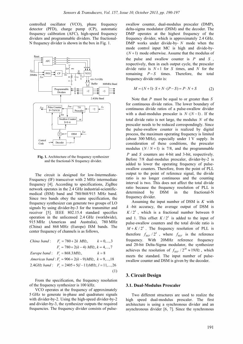
3.2. Pulse-Swallow Counter Fig. 4 shows the block diagram of the
programmable frequency divider. The output of the decoder sets the initial numbers of pulse and swallows counters, while MC is set high and DMP works in divide-by-7 mode. After swallow-counter S counts down to zero, MC is set low and DMP divides by 8. If pulse counter is greater than 0, it continues counting down to zero. Once the pulse counter is equal to zero, swallow counter is reset and a new cycle begins. An inverter is inserted between pulse-swallow counter and the prescaler to remove glitch caused by the delay of MC. The modulus control signal MC, which is the output of pulse-swallow counter and the input of prescaler, lags the output signal outf of prescaler. If the inverter is omitted, a glitch may occur when MC and outf pass through AND gate. As a result, unwanted phase switching happens and the total divide ratio is wrong.
When DSM is disabled, the programmable frequency divider operates in integer mode and initial
numbers of pulse and swallow counters keep constant. When DSM is enabled, the initial numbers of pulse and swallow counters, which are the sum of the decoder output and DSM output, change all the time. The instantaneous divide ratio is not constant while the mean value is equal to the required divide ratio.
Pulse Counter P=7/8/9/10
Swallow CounterS=0~6
MC
En
fPREfDIV 7/8Prescaler ÷2
Decoder
DSM
ControlCode
fDIV
fIN
Fig. 4. Block diagram of the programmable frequency divider.
3.3. Delta-Sigma Modulator In fractional-N frequency synthesizers, fractional
multiples of the reference can be synthesized, allowing a higher reference frequency for a given frequency resolution, therefore, the loop bandwidth can be increased without deteriorating the spectral purity. However, fractional spurs become a problem in fractional-N frequency synthesizers. Several techniques are proposed to minimize fractional spurs and one of them is using Σ∆ modulators [12, 13]. The existence of pattern noise, which is caused by the quantization error, remains a serious problem in the Σ∆ fractional-N frequency synthesizers, where spectral purity is of utmost importance. Several improvements can be made to break the patterns in the Σ∆ modulator output. Moving to higher-order Σ∆ modulators is a first solution to remove the pattern noise. A second option to improve the prediction made by the modulator and further randomize its output is multi-bit quantization instead of single-bit. Another possibility is to add noise, namely dither, to the input signal.
DSM is usually implemented in digital circuit, hence, DSM is a finite state machine (FSM) because it is realized using finite precision arithmetic units and a finite amount of hardware. Without dithering, the DSM is a deterministic FSM with a unique rule for transitioning from each state to the next. In other words, DSM always produces a constant or a periodic output signal when the input is constant. In particular, the period of the signal depends on the input, the initial conditions, and the architecture of the DSM.
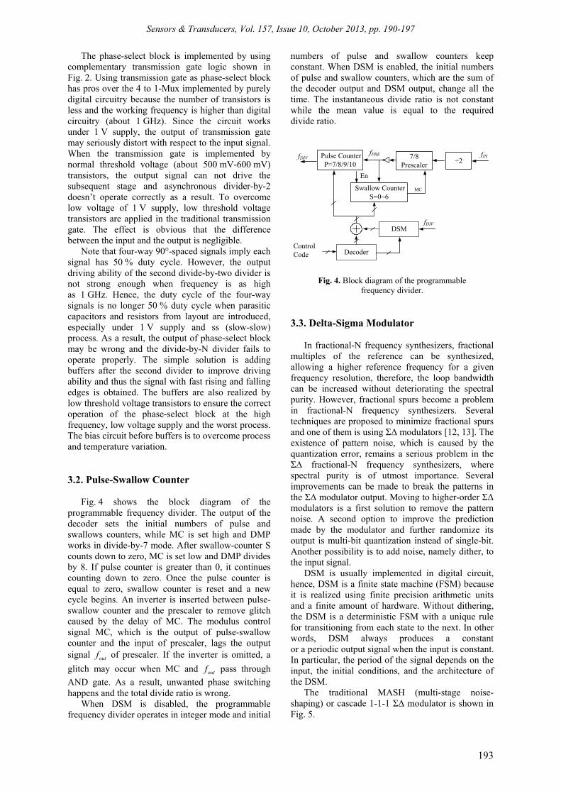
The traditional MASH (multi-stage noise-shaping) or cascade 1-1-1 Σ∆ modulator is shown in Fig. 5.
Sensors & Transducers, Vol. 157, Issue 10, October 2013, pp. 190-197
194
z-1
y1[z]
-e1[z]
z-1
y2[z]
-e2[z]
z-1
y3[z]
-e3[z]
+ ++
z-1-+
++ +
+
z-1-+
+
y[z]
x[z]
Fig. 5. Architecture of MASH 1-1-1 Σ∆ modulator. The Z-domain expression can be written as,
11 1
12 1 2
13 2 3
( ) ( ) (1 ) ( )
( ) ( ) (1 ) ( )
( ) ( ) (1 ) ( )
y z x z z e z
y z e z z e z
y z e z z e z
−
−
−
⎧ = + −⎪
= − + −⎨⎪ = − + −⎩
(3)
And the output is obtained,
1 1 21 2 3
1 33
( ) ( ) (1 ) ( ) (1 ) ( )
( ) (1 ) ( )
y z y z z y z z y z
x z z e z
− −
−
= + − + −
= + − (4)
Then, we have noise transfer function of MASH
1-1-1 Σ∆ modulator,
1 3( ) (1 )NTF z z−= − (5) From equation, the input signal ( )x z keeps the
same in the output ( )y z and the quantization error is moved to high frequency. The order of noise shaping is increased by MASH 1-1-1.
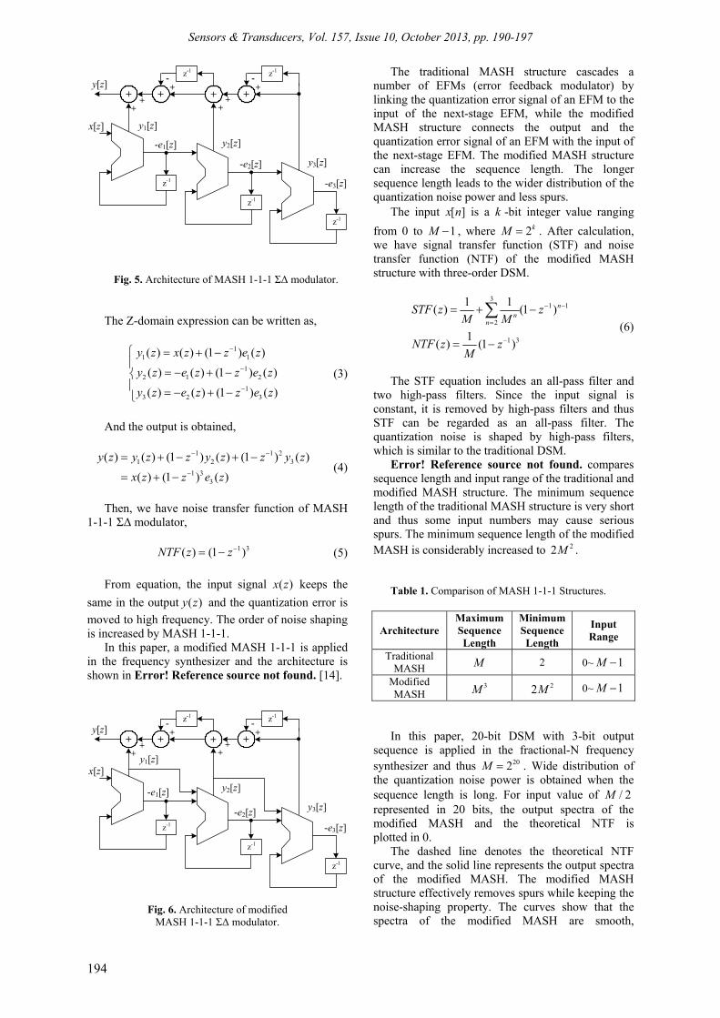
In this paper, a modified MASH 1-1-1 is applied in the frequency synthesizer and the architecture is shown in Error! Reference source not found. [14].
z-1
y1[z]
-e1[z]
z-1
y2[z]
-e2[z]
z-1
y3[z]
-e3[z]
+ ++
z-1-+
++ +
+
z-1-+
+
y[z]
x[z]
Fig. 6. Architecture of modified
MASH 1-1-1 Σ∆ modulator.
The traditional MASH structure cascades a number of EFMs (error feedback modulator) by linking the quantization error signal of an EFM to the input of the next-stage EFM, while the modified MASH structure connects the output and the quantization error signal of an EFM with the input of the next-stage EFM. The modified MASH structure can increase the sequence length. The longer sequence length leads to the wider distribution of the quantization noise power and less spurs.
The input [ ]x n is a k -bit integer value ranging from 0 to 1M − , where 2kM = . After calculation, we have signal transfer function (STF) and noise transfer function (NTF) of the modified MASH structure with three-order DSM.
3
1 1
2
1 3
1 1( ) (1 )
1( ) (1 )
nn
nSTF z z
M M
NTF z zM
− −
=
−
= + −
= −
∑
(6)
The STF equation includes an all-pass filter and
two high-pass filters. Since the input signal is constant, it is removed by high-pass filters and thus STF can be regarded as an all-pass filter. The quantization noise is shaped by high-pass filters, which is similar to the traditional DSM.
Error! Reference source not found. compares sequence length and input range of the traditional and modified MASH structure. The minimum sequence length of the traditional MASH structure is very short and thus some input numbers may cause serious spurs. The minimum sequence length of the modified MASH is considerably increased to 22M .
Table 1. Comparison of MASH 1-1-1 Structures.
Architecture Maximum Sequence Length
Minimum Sequence Length
Input Range
Traditional MASH M 2 0~ 1M −
Modified MASH
3M 22M 0~ 1M −
In this paper, 20-bit DSM with 3-bit output
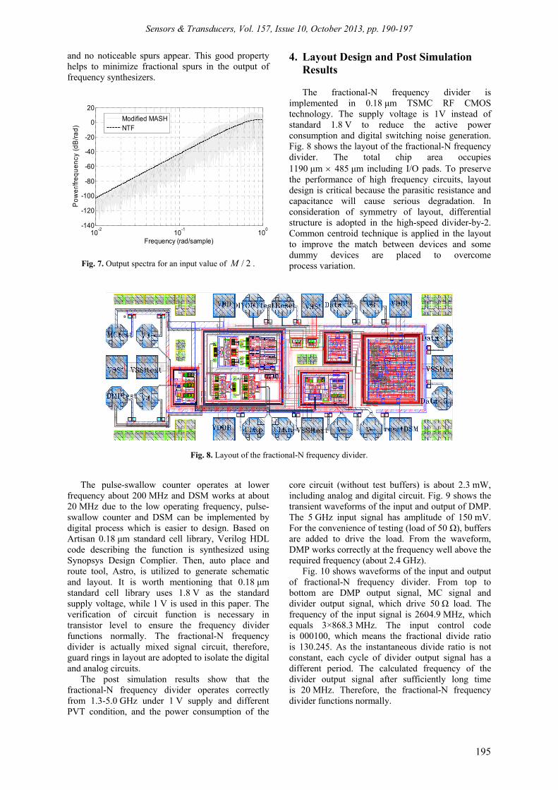
sequence is applied in the fractional-N frequency synthesizer and thus 202M = . Wide distribution of the quantization noise power is obtained when the sequence length is long. For input value of / 2M represented in 20 bits, the output spectra of the modified MASH and the theoretical NTF is plotted in 0.
The dashed line denotes the theoretical NTF curve, and the solid line represents the output spectra of the modified MASH. The modified MASH structure effectively removes spurs while keeping the noise-shaping property. The curves show that the spectra of the modified MASH are smooth,
Sensors & Transducers, Vol. 157, Issue 10, October 2013, pp. 190-197
195
and no noticeable spurs appear. This good property helps to minimize fractional spurs in the output of frequency synthesizers.
10-2 10-1 100-140
-120
-100
-80
-60
-40
-20
0
20
Frequency (rad/sample)
Pow
er/fr
eque
ncy
(dB
/rad)
Modified MASHNTF
Fig. 7. Output spectra for an input value of / 2M .
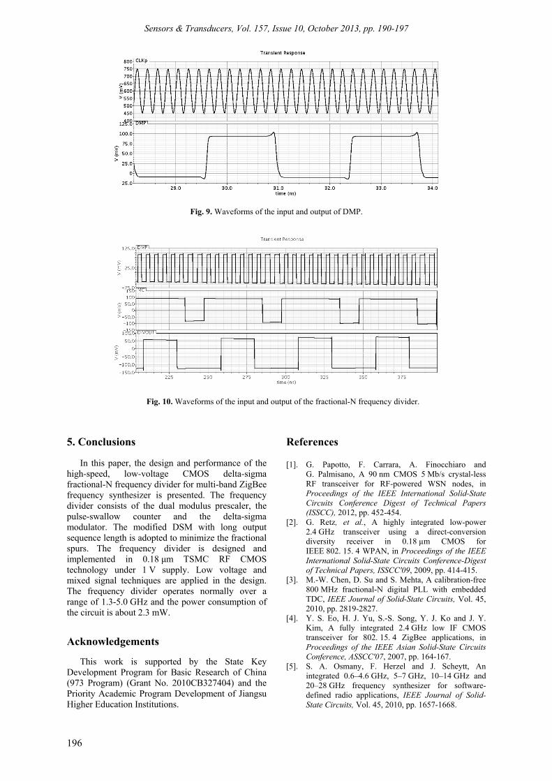
4. Layout Design and Post Simulation Results The fractional-N frequency divider is
implemented in 0.18 µm TSMC RF CMOS technology. The supply voltage is 1V instead of standard 1.8 V to reduce the active power consumption and digital switching noise generation. Fig. 8 shows the layout of the fractional-N frequency divider. The total chip area occupies 1190 µm × 485 µm including I/O pads. To preserve the performance of high frequency circuits, layout design is critical because the parasitic resistance and capacitance will cause serious degradation. In consideration of symmetry of layout, differential structure is adopted in the high-speed divider-by-2. Common centroid technique is applied in the layout to improve the match between devices and some dummy devices are placed to overcome process variation.
Fig. 8. Layout of the fractional-N frequency divider.
The pulse-swallow counter operates at lower frequency about 200 MHz and DSM works at about 20 MHz due to the low operating frequency, pulse-swallow counter and DSM can be implemented by digital process which is easier to design. Based on Artisan 0.18 µm standard cell library, Verilog HDL code describing the function is synthesized using Synopsys Design Complier. Then, auto place and route tool, Astro, is utilized to generate schematic and layout. It is worth mentioning that 0.18 µm standard cell library uses 1.8 V as the standard supply voltage, while 1 V is used in this paper. The verification of circuit function is necessary in transistor level to ensure the frequency divider functions normally. The fractional-N frequency divider is actually mixed signal circuit, therefore, guard rings in layout are adopted to isolate the digital and analog circuits.
The post simulation results show that the fractional-N frequency divider operates correctly from 1.3-5.0 GHz under 1 V supply and different PVT condition, and the power consumption of the
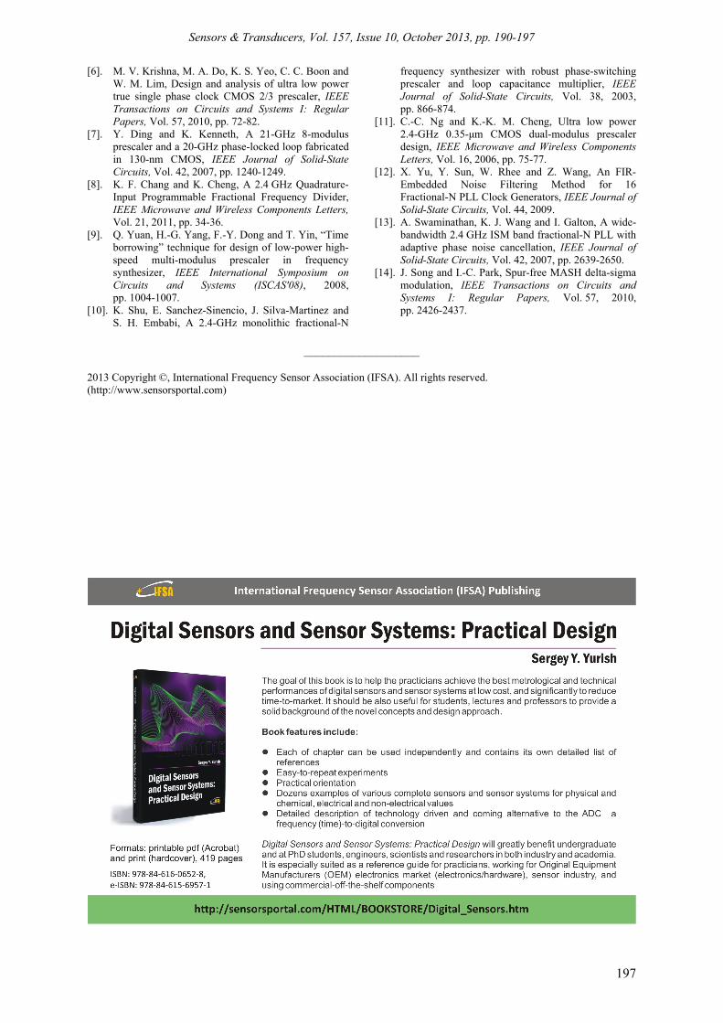
core circuit (without test buffers) is about 2.3 mW, including analog and digital circuit. Fig. 9 shows the transient waveforms of the input and output of DMP. The 5 GHz input signal has amplitude of 150 mV. For the convenience of testing (load of 50 Ω), buffers are added to drive the load. From the waveform, DMP works correctly at the frequency well above the required frequency (about 2.4 GHz).
Fig. 10 shows waveforms of the input and output of fractional-N frequency divider. From top to bottom are DMP output signal, MC signal and divider output signal, which drive 50 Ω load. The frequency of the input signal is 2604.9 MHz, which equals 3×868.3 MHz. The input control code is 000100, which means the fractional divide ratio is 130.245. As the instantaneous divide ratio is not constant, each cycle of divider output signal has a different period. The calculated frequency of the divider output signal after sufficiently long time is 20 MHz. Therefore, the fractional-N frequency divider functions normally.
Sensors & Transducers, Vol. 157, Issue 10, October 2013, pp. 190-197
196
Fig. 9. Waveforms of the input and output of DMP.
Fig. 10. Waveforms of the input and output of the fractional-N frequency divider.
5. Conclusions In this paper, the design and performance of the
high-speed, low-voltage CMOS delta-sigma fractional-N frequency divider for multi-band ZigBee frequency synthesizer is presented. The frequency divider consists of the dual modulus prescaler, the pulse-swallow counter and the delta-sigma modulator. The modified DSM with long output sequence length is adopted to minimize the fractional spurs. The frequency divider is designed and implemented in 0.18 µm TSMC RF CMOS technology under 1 V supply. Low voltage and mixed signal techniques are applied in the design. The frequency divider operates normally over a range of 1.3-5.0 GHz and the power consumption of the circuit is about 2.3 mW.
Acknowledgements This work is supported by the State Key
Development Program for Basic Research of China (973 Program) (Grant No. 2010CB327404) and the Priority Academic Program Development of Jiangsu Higher Education Institutions.
References [1]. G. Papotto, F. Carrara, A. Finocchiaro and
G. Palmisano, A 90 nm CMOS 5 Mb/s crystal-less RF transceiver for RF-powered WSN nodes, in Proceedings of the IEEE International Solid-State Circuits Conference Digest of Technical Papers (ISSCC), 2012, pp. 452-454.
[2]. G. Retz, et al., A highly integrated low-power 2.4 GHz transceiver using a direct-conversion diversity receiver in 0.18 µm CMOS for IEEE 802. 15. 4 WPAN, in Proceedings of the IEEE International Solid-State Circuits Conference-Digest of Technical Papers, ISSCC'09, 2009, pp. 414-415.
[3]. M.-W. Chen, D. Su and S. Mehta, A calibration-free 800 MHz fractional-N digital PLL with embedded TDC, IEEE Journal of Solid-State Circuits, Vol. 45, 2010, pp. 2819-2827.
[4]. Y. S. Eo, H. J. Yu, S.-S. Song, Y. J. Ko and J. Y. Kim, A fully integrated 2.4 GHz low IF CMOS transceiver for 802. 15. 4 ZigBee applications, in Proceedings of the IEEE Asian Solid-State Circuits Conference, ASSCC'07, 2007, pp. 164-167.
[5]. S. A. Osmany, F. Herzel and J. Scheytt, An integrated 0.6–4.6 GHz, 5–7 GHz, 10–14 GHz and 20–28 GHz frequency synthesizer for software-defined radio applications, IEEE Journal of Solid-State Circuits, Vol. 45, 2010, pp. 1657-1668.
Sensors & Transducers, Vol. 157, Issue 10, October 2013, pp. 190-197
197
[6]. M. V. Krishna, M. A. Do, K. S. Yeo, C. C. Boon and W. M. Lim, Design and analysis of ultra low power true single phase clock CMOS 2/3 prescaler, IEEE Transactions on Circuits and Systems I: Regular Papers, Vol. 57, 2010, pp. 72-82.
[7]. Y. Ding and K. Kenneth, A 21-GHz 8-modulus prescaler and a 20-GHz phase-locked loop fabricated in 130-nm CMOS, IEEE Journal of Solid-State Circuits, Vol. 42, 2007, pp. 1240-1249.
[8]. K. F. Chang and K. Cheng, A 2.4 GHz Quadrature-Input Programmable Fractional Frequency Divider, IEEE Microwave and Wireless Components Letters, Vol. 21, 2011, pp. 34-36.
[9]. Q. Yuan, H.-G. Yang, F.-Y. Dong and T. Yin, “Time borrowing” technique for design of low-power high-speed multi-modulus prescaler in frequency synthesizer, IEEE International Symposium on Circuits and Systems (ISCAS'08), 2008, pp. 1004-1007.
[10]. K. Shu, E. Sanchez-Sinencio, J. Silva-Martinez and S. H. Embabi, A 2.4-GHz monolithic fractional-N
frequency synthesizer with robust phase-switching prescaler and loop capacitance multiplier, IEEE Journal of Solid-State Circuits, Vol. 38, 2003, pp. 866-874.
[11]. C.-C. Ng and K.-K. M. Cheng, Ultra low power 2.4-GHz 0.35-µm CMOS dual-modulus prescaler design, IEEE Microwave and Wireless Components Letters, Vol. 16, 2006, pp. 75-77.
[12]. X. Yu, Y. Sun, W. Rhee and Z. Wang, An FIR-Embedded Noise Filtering Method for 16 Fractional-N PLL Clock Generators, IEEE Journal of Solid-State Circuits, Vol. 44, 2009.
[13]. A. Swaminathan, K. J. Wang and I. Galton, A wide-bandwidth 2.4 GHz ISM band fractional-N PLL with adaptive phase noise cancellation, IEEE Journal of Solid-State Circuits, Vol. 42, 2007, pp. 2639-2650.
[14]. J. Song and I.-C. Park, Spur-free MASH delta-sigma modulation, IEEE Transactions on Circuits and Systems I: Regular Papers, Vol. 57, 2010, pp. 2426-2437.
___________________
2013 Copyright ©, International Frequency Sensor Association (IFSA). All rights reserved. (http://www.sensorsportal.com)
Related Documents


![Jestrjestr.org/downloads/Volume6Issue5/fulltext14652013.pdf · can realize the even frequency division easily [2-5], but it is difficult to realize odd frequency divider and fractional](https://static.cupdf.com/doc/110x72/5ea1dc9af38ba7320c7fd2ad/can-realize-the-even-frequency-division-easily-2-5-but-it-is-difficult-to-realize.jpg)