N. Senthil Kumar, M. Saravanan & S. Jeevananthan © Oxford University Press 2013

354 33 Powerpoint-slides CH5
Dec 28, 2015
microcontroller ppt
Welcome message from author
This document is posted to help you gain knowledge. Please leave a comment to let me know what you think about it! Share it to your friends and learn new things together.
Transcript
N. Senthil Kumar,M. Saravanan & S. Jeevananthan
© Oxford University Press 2013
© Oxford University Press 2013
Hardware Interfacing with Intel 8085
© Oxford University Press 2013
Methods of Data Transfer and Interrupt Structure in
8085
• Data transfer in any microprocessor based system is essential.
• The data transfer can take place between processor and memory or between processor and input device or between processor and output device or between memory and input device or between memory and output device.
• Data can be transferred in many different ways in all these data transfers.
Data transfer mechanisms
© Oxford University Press 2013
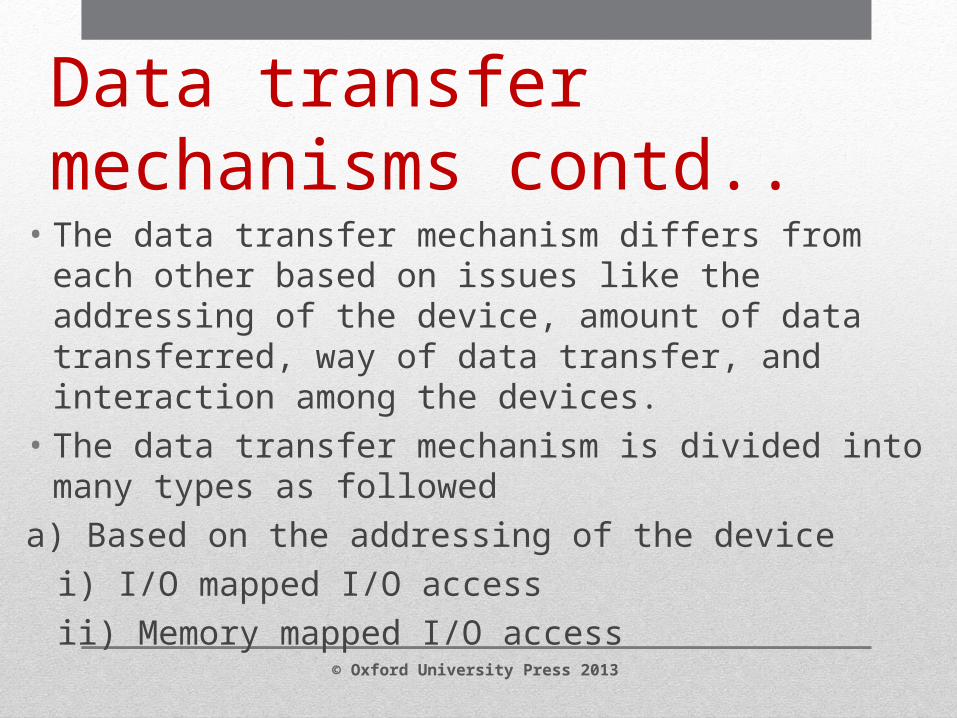
• The data transfer mechanism differs from each other based on issues like the addressing of the device, amount of data transferred, way of data transfer, and interaction among the devices.
• The data transfer mechanism is divided into many types as followed
a) Based on the addressing of the devicei) I/O mapped I/O access ii) Memory mapped I/O access
Data transfer mechanisms contd..
© Oxford University Press 2013
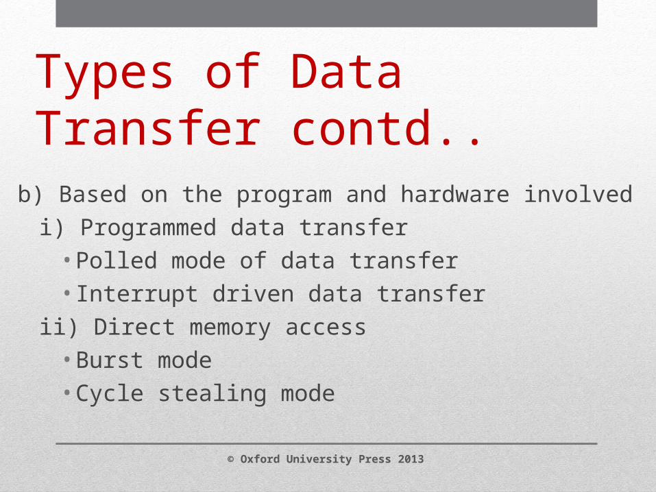
b) Based on the program and hardware involvedi) Programmed data transfer• Polled mode of data transfer• Interrupt driven data transfer
ii) Direct memory access• Burst mode• Cycle stealing mode
Types of Data Transfer contd..
© Oxford University Press 2013
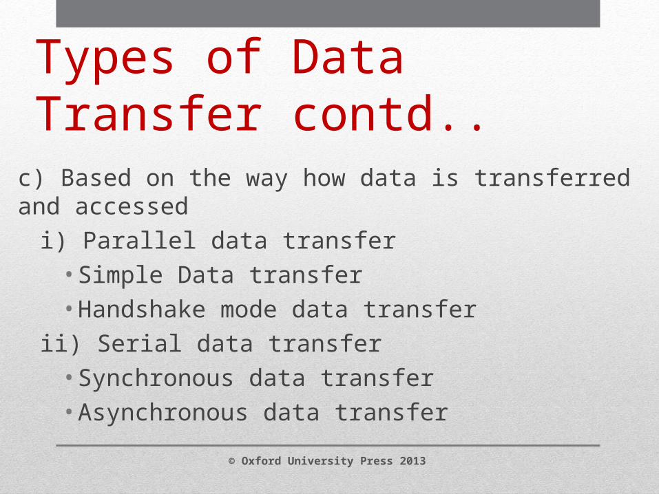
c) Based on the way how data is transferred and accessedi) Parallel data transfer• Simple Data transfer• Handshake mode data transfer
ii) Serial data transfer• Synchronous data transfer• Asynchronous data transfer
Types of Data Transfer contd..
© Oxford University Press 2013
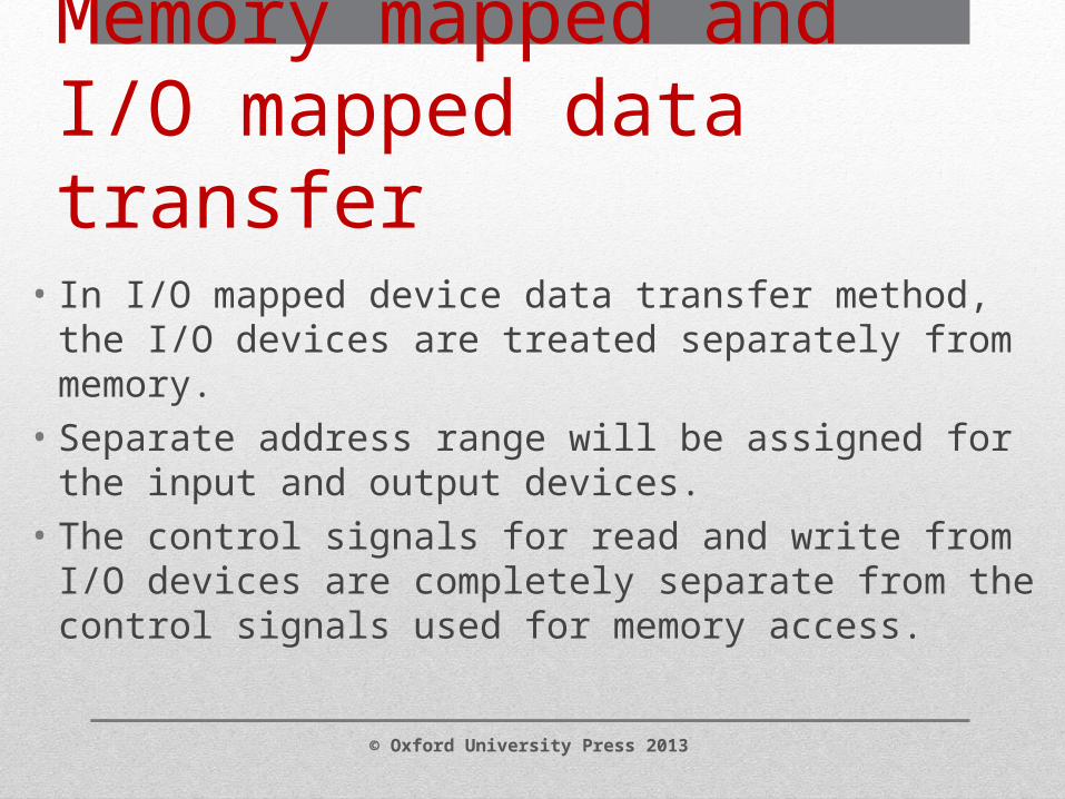
• In I/O mapped device data transfer method, the I/O devices are treated separately from memory.
• Separate address range will be assigned for the input and output devices.
• The control signals for read and write from I/O devices are completely separate from the control signals used for memory access.
Memory mapped and I/O mapped data transfer
© Oxford University Press 2013
© Oxford University Press 2013
Memory mapped and I/O mapped data transfer
• The microprocessor will have separate instructions for Input and output device access such as IN instruction and OUT instruction of 8085.
• As the memory and I/O device access is completely different, a single address can be assigned to both an I/O device and a memory location.
• In memory mapped I/O, each input device or output device is treated as if it is a memory location.
• The control signal for read and write operation of I/O device is same as that of memory chips.
• Each input or output device is identified by a unique address in the memory address range.
Memory Mapped I/O
© Oxford University Press 2013
© Oxford University Press 2013
Memory Mapped I/O
• All the memory related instructions used to read data from memory are used to access input and output device.
• Since the I/O devices use some of the memory address space, the maximum memory addressing capacity will be reduced in a microprocessor based system.
• Programmed data transfer is written and controlled by programmer and executed by the processor.
• The data transfer between processor and I/O devices or vice versa takes place by executing the corresponding instruction.
• Programmed I/O data transfers are identical to read and write operations for memories or device registers.
• An example of programmed I/O is a device driver writing one data byte at a time directly to the device's memory.
Programmed data transfer
© Oxford University Press 2013
• The execution of programmed data transfer can take place at predefined period determined by the programmer.
• Based the time of execution of the data transfer instruction, the programmed data transfer is divided into two types namelya) Polled mode of data transfer b) Interrupt driven data transfer
Programmed data transfer contd..
© Oxford University Press 2013
• In polled mode of data transfer, the data is read from an input device when the processor or CPU is ready and executes the data transfer instruction.
• If the input device is not ready the processor will wait until the device is ready with data.
Polled mode of data transfer
© Oxford University Press 2013
© Oxford University Press 2013
Polled mode of data transfer
• Similarly, the data is written into an output device by the processor when it executes the data ‘write’ instruction to the corresponding output device.
• The program is written in such a way that the processor will wait in a loop until the output device is ready to receive data.
• As it can be seen clearly, the processor time is wasted in this polled mode of data transfer as it waits for the device to be ready.
• In interrupt driven data transfer, the data is read from the input device only when the input device is ready with data.
• When the device is ready, it will give a signal to interrupt the processor indicating that the data is ready.
• In the interrupt service routine, the program is written to read the data from the corresponding input device.
• Similarly, the output device will also give an interrupt to the processor when it can accept a data.
• The programmers have to write an interrupt service routine for data transfer to the corresponding output device.
Interrupt driven data transfer
© Oxford University Press 2013
• In programmed I/O data transfer, processor is actively involved in the entire data transfer process. The processor is tied up and processor time is wasted. So, the data transfer rate is limited.
• To overcome these disadvantages of programmed data transfer and to increase the speed of data transfer, DMA method of data transfer is used.
Direct Memory Access (DMA)
© Oxford University Press 2013
• Peripheral or DMA controller asserts one of the request pins for holding the processor, e.g., HOLD
• The processor completes its current instruction and enters into a HOLD state.
• In hold state, the processor temporarily stops the execution of the instruction and releases the address and data bus by making them enter into a high impedance state.
Sequence of events of a typical DMA process
© Oxford University Press 2013
© Oxford University Press 2013
Sequence of events of a typical DMA process
• The processor issues a ‘Hold Acknowledge’ (HLDA) signal as a token of releasing of bus control to the peripheral or DMA controller.
• DMA operation starts.• Upon completion of the DMA operation, the peripheral or
DMA controller removes the HOLD signal applied to the processor and relinquishes bus control.
• A DMA controller can in general interface several peripherals that may request DMA with the processor.
• The controller decides the priority of simultaneous DMA requests from many peripherals.
• It then communicates with the peripheral and the CPU, and provides memory addresses for data transfer.
DMA Controller
© Oxford University Press 2013
© Oxford University Press 2013
DMA Controller
• DMA controller commonly used with 8085 and 8088 processors is the 8237 programmable DMA controller device.
• The 8237 is a 4-channel device. Each channel is dedicated to a specific peripheral device and capable of addressing 64 K bytes section of memory.
• In parallel mode of data transfer, all the bits in a word are simultaneously transmitted in parallel.
• In 8085, a word is made of 8 bits and 8 bits are transmitted and received in parallel form.
• In some special cases, the number of data bits transferred will be less in number.
Parallel data transfer
© Oxford University Press 2013
© Oxford University Press 2013
Parallel data transfer• The parallel data transfer is used in general for transfer of
data over short distances such as within a system or within a board etc.
• The parallel data transfer can be done eithera)By polled mode b)By interrupt driven mode.In polled method, the data is read from the input device by
the processor at a time determined by the processor. • This polled mode of data transfer can be done in two ways
–a) synchronous or b) simple I/O and Handshake I/O.
• In simple or synchronous mode, the data is read from the input device by the processor irrespective of the status of the input device.
• It is assumed that the input device is ready with the data as and when the processor reads the data and the input device is in synchronism with the processor.
• Similarly, the data is written into the output device irrespective of its status assuming that the output device is in synchronism with the processor.
Parallel data transfer contd..
© Oxford University Press 2013
• Drawback of parallel data transfer:a) The parallel data transfer has the drawback of many wires needed
to transfer all the bits of data. b) So, the parallel data transfer can not be effectively used for long
distance transfers. c) As one wire is used for each bit, byte wise data transfers are eight
times more expensive than a single bit transfer. • Serial data transfer is the solution for data transfers over long
distances. • Also, serial communications are low cost way to send data over
long distances.
© Oxford University Press 2013
Parallel data transfer contd..
• In serial data transfer, only one bit is transferred over a data transfer line.
• All the bits in a data word can be transmitted by using a shift register and transferring the data bit by bit.
• So, the important parameter in serial data transfer is the clock frequency at which the bit data are transmitted into the serial data line.
• The frequency at which the data is transmitted serially is technically as baud rate.
Serial data transfer
© Oxford University Press 2013
• Baud rate is the measure of the number of bits transmitted over a second.
• The parallel to serial data conversion is done by a device called Universal Asynchronous Receiver-Transmitter (UART).
• The serial data transfer can be done in two modesa) the synchronous mode and b) the asynchronous mode.
• In synchronized data transfer, the device which sends the data and the device which receives the data are synchronized with the common clock.
Serial data transfer contd..
© Oxford University Press 2013
• In synchronous mode, the data transfer takes place with a fixed and known time frame.
• In asynchronous data transfer, the data words are transmitted with a random time frame between them.
• Most of the microprocessor and computer related data communications are based upon the asynchronous mode of transmissions.
• The microprocessor uses interrupts and other software techniques to synchronize random timing between data words to receive the data completely.
© Oxford University Press 2013
Serial data transfer contd..
• RS – 232 is one of the most widely techniques used to interface external equipment to computers.
• It uses serial communications where one bit is sent along a line, at a time.
• RS-232 is the interface for computer to talk to and exchange data with modem and other serial devices.
RS232 Standard
© Oxford University Press 2013
© Oxford University Press 2013
RS232 Standard
• The main advantage that serial communication has over parallel communications is that single wire is needed to transmit and another to receive.
• RS232 is an interface to connect one DTE, data terminal equipment to one DCE, data communication equipment at a maximum speed of 20 kbps with a maximum cable length of 50 feet.
• The Electronic Industries Association (EIA), an industry trade group, defined RS232 originally for teletypewriter devices.
• Many people, however, still refer to the standard as RS-232C, or just RS- 232.
• The electrical characteristics of RS-232 define the minimum voltages of logic ‘1’ and ‘0’ transmission. Logic ‘1’ ranges from -3 V to -25 V, but will typically be around -12 V. A logical ‘0’ ranges from 3V to 25V, but will typically around -12V.
• If no pulses are present on the line, the voltage level is equivalent to a high level, that is -12V.
RS232 Standard
© Oxford University Press 2013
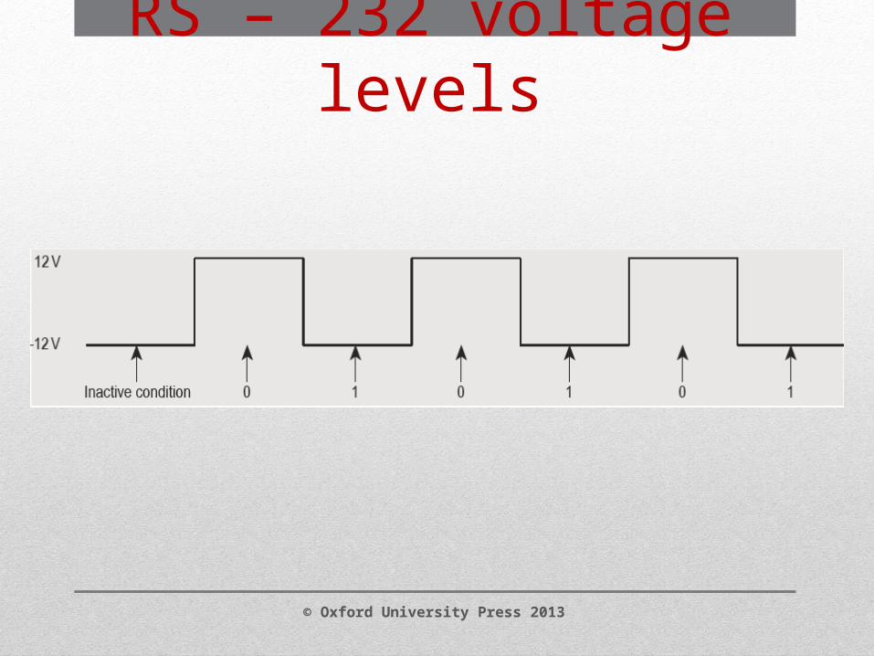
RS – 232 voltage levels
© Oxford University Press 2013
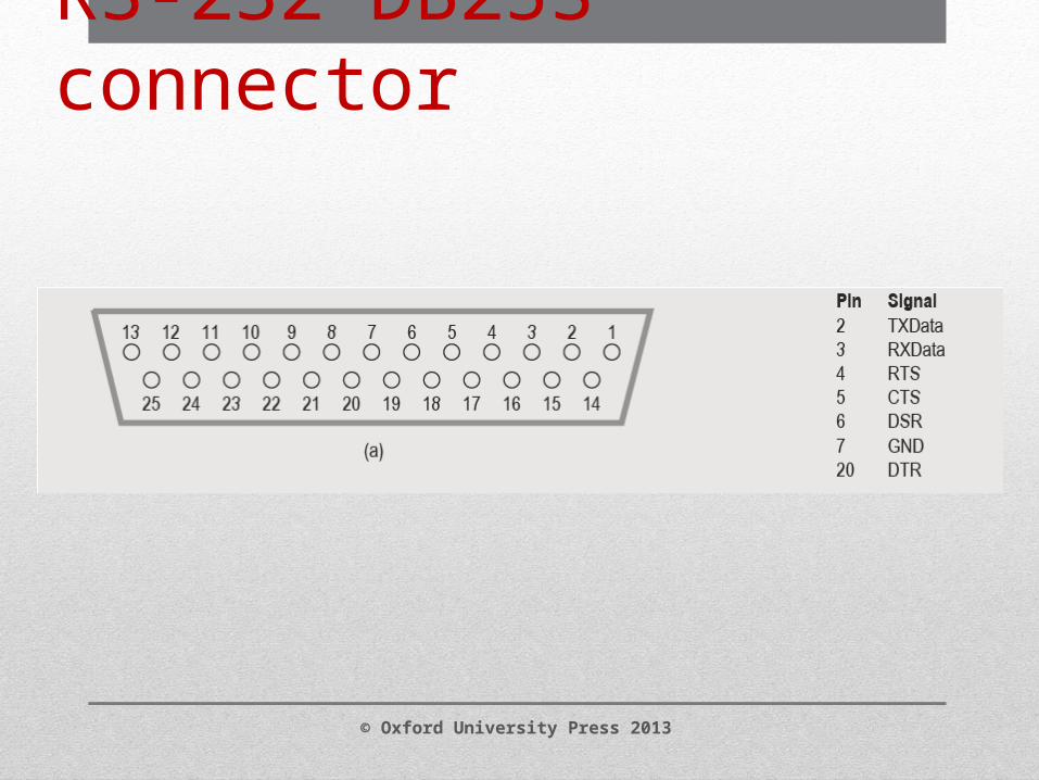
RS-232 DB25S connector
© Oxford University Press 2013
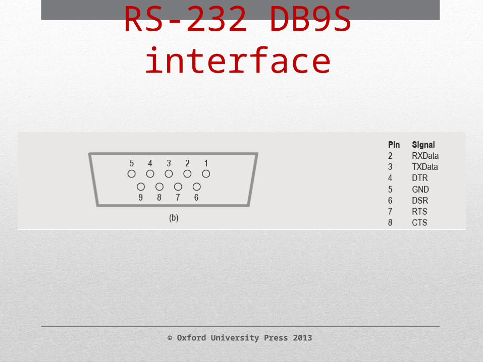
RS-232 DB9S interface
© Oxford University Press 2013
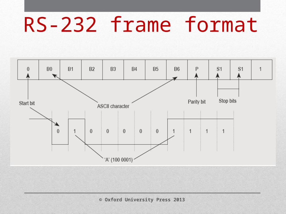
RS-232 frame format
© Oxford University Press 2013
• Error control is bit data added to transmitted byte data in order to detect or correct an error in transmission.
• RS-232 uses a simple technique known as parity to provide minimum possible error detection.
• A parity bit is added to the transmitted data to make the number of 1s sent as either even (even parity) or odd (odd parity).
• It is a simple method of error coding and only requires exclusive - OR (XOR) gates to generate the parity bit.
Parity
© Oxford University Press 2013
• The parity bit is added to the transmitted data by inserting it into the shift register at the correct bit position.
• A single parity bit can only detect an odd number of errors, that is, 1, 3, 5, and so on.
• If there is an even number of error bits then the parity bit will be correct and no error will be detected.
Parity cond..
© Oxford University Press 2013
• One of the main parameters, which specify RS-232 communications, is the rate of transmission at which data is transmitted and received.
• It is important that the transmitter and receiver operate at the same speed.
• For asynchronous transmission, the start and stop bits are added in addition to the 7 ASCII character bits and the parity.
• Thus a total of 10 bits are required to transmit a single character. With 2 stop bits, a total of 11 bits are required.
Baud rate and bit stream timings
© Oxford University Press 2013
• If 10 characters are sent every second, and if 11 bits are used for each character, then the transmission rate is 110 bits per second (bps).
• In addition to the bit rate, another term used to describe the transmission speed is the baud rate.
Baud rate and bit stream timings
© Oxford University Press 2013
© Oxford University Press 2013
Baud rate and bit stream timings• The bit rate refers to the actual rate at which bits are
transmitted, whereas the baud rate relates to the rate at which signalling elements are transmitted.
• The signalling elements are used to represent bits. As one signalling element encodes one bit, the bits per second and baud rate are identical.
• Only in modems, the bit rate differs from the baud rate.
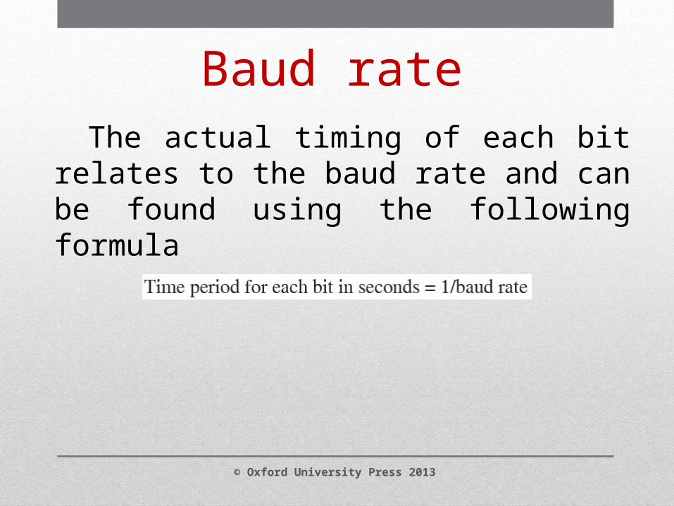
Baud rate
The actual timing of each bit relates to the baud rate and can be found using the following formula
© Oxford University Press 2013
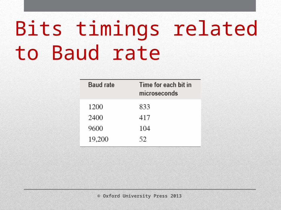
Bits timings related to Baud rate
© Oxford University Press 2013
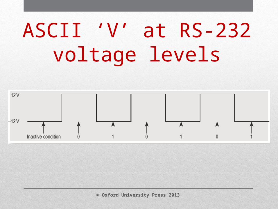
ASCII ‘V’ at RS-232 voltage levels
© Oxford University Press 2013
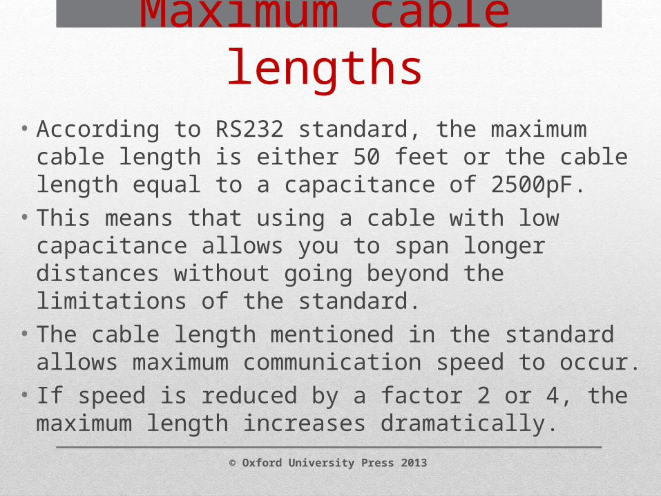
• According to RS232 standard, the maximum cable length is either 50 feet or the cable length equal to a capacitance of 2500pF.
• This means that using a cable with low capacitance allows you to span longer distances without going beyond the limitations of the standard.
• The cable length mentioned in the standard allows maximum communication speed to occur.
• If speed is reduced by a factor 2 or 4, the maximum length increases dramatically.
Maximum cable lengths
© Oxford University Press 2013
• RS-232 is intended to be a standard but not all manufacturers abide by it.
• Some implement the full specification while others implement just a partial specification.
• This is mainly because not every device requires the full functionality of RS-232, for example a modem requires many more control lines than a serial mouse.
RS232 Communications between two nodes
© Oxford University Press 2013
© Oxford University Press 2013
RS232 Communications between two nodes
• The rate at which data is transmitted and the speed at which the transmitter and receiver can transmit/receive the data dictates whether data handshaking is required.
• In the transmission of data, there can either be no handshaking, hardware handshaking or software handshaking.
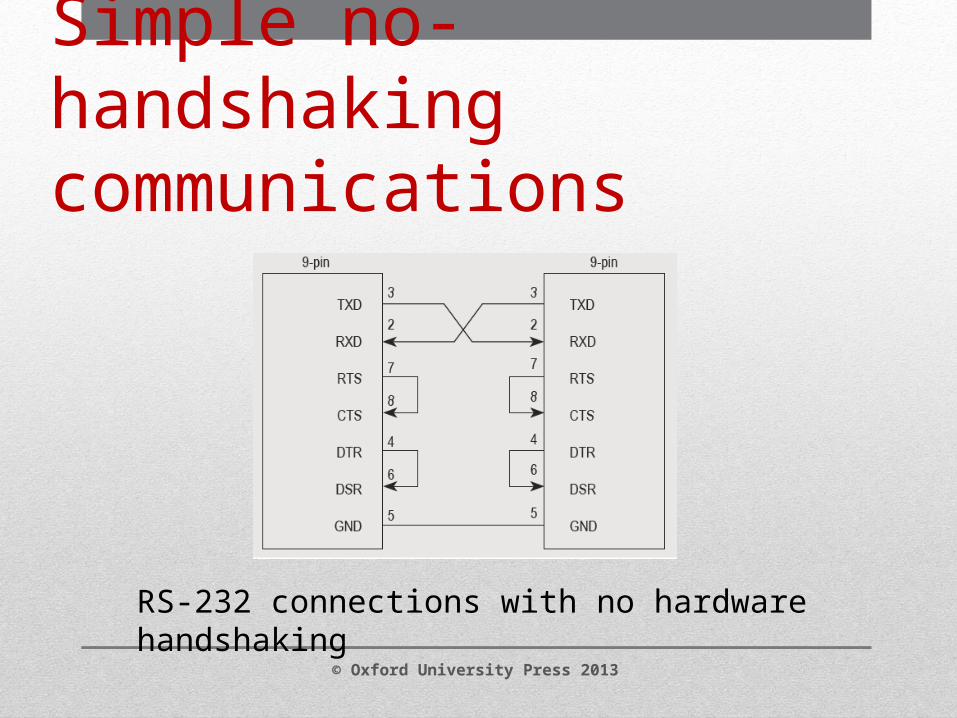
Simple no-handshaking communications
RS-232 connections with no hardware handshaking
© Oxford University Press 2013
Hardware handshaking
© Oxford University Press 2013
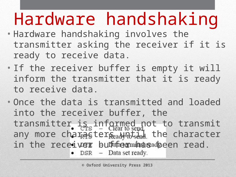
• Hardware handshaking involves the transmitter asking the receiver if it is ready to receive data.
• If the receiver buffer is empty it will inform the transmitter that it is ready to receive data.
• Once the data is transmitted and loaded into the receiver buffer, the transmitter is informed not to transmit any more characters until the character in the receiver buffer has been read.
• RS232, RS422, RS423 and RS485 are serial communication methods for computers and devices.
• RS232 is the best known interface, because this serial interface is implemented on almost all computers available today.
• But some of the other interfaces are certainly interesting because they can be used in situations where RS232 is not appropriate.
Introduction to RS485 Standard
© Oxford University Press 2013
• RS232 is an interface to connect one DTE, data terminal equipment to one DCE, data communication equipment at a maximum speed of 20 kbps with a maximum cable length of 50 feet.
• This was sufficient in the old days where almost all computer equipment were connected using modems.
RS232- Introduction
© Oxford University Press 2013
© Oxford University Press 2013
RS232- Introduction
• But sooner people started to look for interfaces capable of one or more of the following
a)Connect DTE's directly without the need of modemsb)Connect several DTE's in a network structure c)Ability to communicate over longer distances d)Ability to communicate at faster communication rates
• The RS485 signals are floating and each signal is transmitted over a Sig+ line and a Sig- line.
• The RS485 receiver compares the voltage difference between both lines, instead of the absolute voltage level on a signal line.
• This works well and prevents the existence of ground loops, a common source of communication problems.
• The best results are achieved if the Sig+ and Sig- lines are twisted lines as shown in figure
RS485 - Introduction
© Oxford University Press 2013
• If high noise immunity is needed, often a combination of twisting and shielding is used as for example in STP, shielded twisted pair and FTP, foiled twisted pair networking cables.
• Differential signals and twisting allows RS485 to communicate over much longer communication distances than achievable with RS232.
• With RS485 communication distances of 1200 m are possible.
Noise in straight and twisted pair cable contd..
© Oxford University Press 2013
• The speed of the differential interfaces RS422 and RS485 is far superior to the single ended versions RS232 and RS423.
• There is a maximum slew rate defined for both RS232 and RS423. • This has been done to avoid reflections of signals.
Characteristics of RS485 compared to RS232, RS422 and RS423
© Oxford University Press 2013
© Oxford University Press 2013
Characteristics of RS485 compared to RS232, RS422 and RS423
• The maximum slew rate also limits the maximum communication speed on the line.
• For both other interfaces—RS422 and RS485—the slew rate is indefinite.
• To avoid reflections on longer cables it is necessary to use appropriate termination resistors.
• Interesting is, that RS232 is the only interface capable of full duplex communication.
• This is, because on the other interfaces the communication channel is shared by multiple receivers and—in the case of RS485—by multiple senders.
• RS232 has a separate communication line for transmitting and receiving which—with a well written protocol—allows higher effective data rates at the same bit rate than the other interfaces.
• The request and acknowledge data needed in most protocols does not consume bandwidth on the primary data channel of RS232.
Characteristics of RS485 compared to RS232, RS422 and RS423 contd..
© Oxford University Press 2013
• Network topology is probably the reason why RS485 is now the favorite of the four mentioned interfaces in data acquisition and control applications.
• RS485 is the only of the interfaces capable of internetworking multiple transmitters and receivers in the same network.
• When using the default RS485 receivers with an input resistance of 12 kΩ it is possible to connect 32 devices to the network.
Network topology with RS485
© Oxford University Press 2013
• Default, all the senders on the RS485 bus are in tri-state with high impedance.
• In most higher level protocols, one of the nodes is defined as a master which sends queries or commands over the RS485 bus.
• All other nodes receive these data. Depending of the information in the sent data, zero or more nodes on the line respond to the master. In this situation, bandwidth can be used for almost 100%.
• There are other implementations of RS485 networks where every node can start a data session on its own.
RS485 operation
© Oxford University Press 2013
• There is no need for the senders to explicitly turn the RS485 driver on or off.
• RS485 drivers automatically return to their high impedance tri-state within a few microseconds after the data has been sent.
• Therefore it is not needed to have delays between the data packets on the RS485 bus.
• RS485 is used as the electrical layer for many well known interface standards, including Profibus and Modbus.
• Therefore RS485 will be in use for many years in the future.
RS485 operation contd..
© Oxford University Press 2013
• GPIB devices communicate with other GPIB devices by sending device-dependent messages and interface messages through the interface system.
• Device-dependent messages, often called data or data messages, contain device-specific information, such as programming instructions, measurement results, machine status, and data files.
• Interface messages manage the bus. Usually called commands or command messages, interface messages perform such functions as initializing the bus, addressing and unaddressing devices, and setting device modes for remote or local programming.
GPIB Standard
© Oxford University Press 2013
• GPIB Devices can be Talkers, Listeners, and/or Controllers. • A Talker sends data messages to one or more Listeners,
which receive the data. • The Controller manages the flow of information on the GPIB
by sending commands to all devices. • A digital voltmeter, for example, is a Talker and is also a
Listener. • The GPIB is like an ordinary computer bus, except that a
computer has its circuit cards interconnected via a backplane - the GPIB has stand-alone devices interconnected by standard cables.
GPIB Standard contd..
© Oxford University Press 2013
• The GPIB interface system consists of 16 signal lines and eight ground-return or shield-drain lines.
• The 16 signal lines, discussed below, are grouped into data lines (eight), handshake lines (three), and interface management lines (five) as shown in Figure
• The eight data lines, DIO1 through DIO8, carry both data and command messages. The state of the Attention (ATN) line determines whether the information is data or commands.
• All commands and most data use the 7-bit ASCII or ISO code set, in which case the eighth bit, DIO8, is either unused or used for parity.
GPIB Signals and Lines
© Oxford University Press 2013
• It guarantees that message bytes on the data lines are sent and received without transmission error.
• NRFD (not ready for data) - Indicates when a device is ready or not ready to receive a message byte. The line is driven by all devices when receiving commands, by Listeners when receiving data messages, and by the Talker when enabling the HS488 protocol.
GPIB Signals and Lines
© Oxford University Press 2013
© Oxford University Press 2013
GPIB Signals and Lines
• NDAC (not data accepted) - Indicates when a device has or has not accepted a message byte. The line is driven by all devices when receiving commands, and by Listeners when receiving data messages.
• DAV (data valid) - Tells when the signals on the data lines are stable (valid) and can be accepted safely by devices. The Controller drives DAV when sending commands, and the Talker drives DAV when sending data messages.
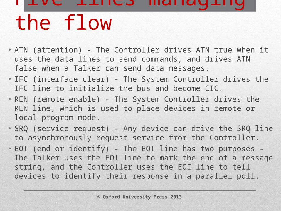
• ATN (attention) - The Controller drives ATN true when it uses the data lines to send commands, and drives ATN false when a Talker can send data messages.
• IFC (interface clear) - The System Controller drives the IFC line to initialize the bus and become CIC.
• REN (remote enable) - The System Controller drives the REN line, which is used to place devices in remote or local program mode.
• SRQ (service request) - Any device can drive the SRQ line to asynchronously request service from the Controller.
• EOI (end or identify) - The EOI line has two purposes - The Talker uses the EOI line to mark the end of a message string, and the Controller uses the EOI line to tell devices to identify their response in a parallel poll.
Five lines managing the flow
© Oxford University Press 2013
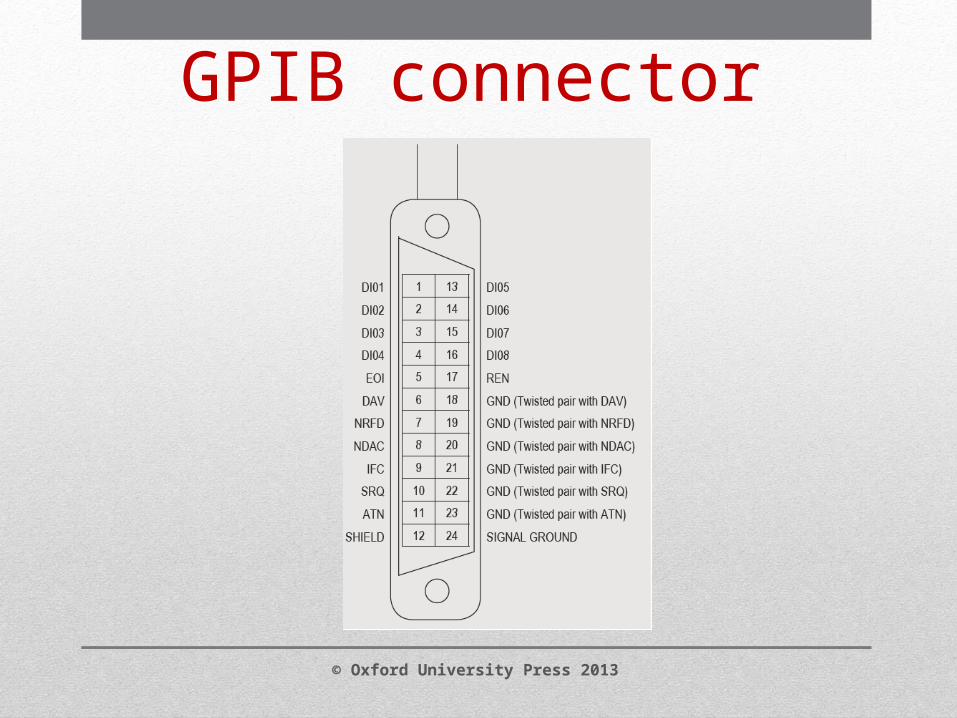
GPIB connector
© Oxford University Press 2013
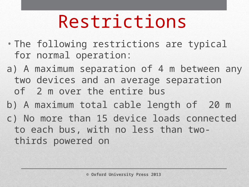
• The following restrictions are typical for normal operation: a) A maximum separation of 4 m between any two devices
and an average separation of 2 m over the entire bus b) A maximum total cable length of 20 m c) No more than 15 device loads connected to each bus, with
no less than two-thirds powered on
Restrictions
© Oxford University Press 2013
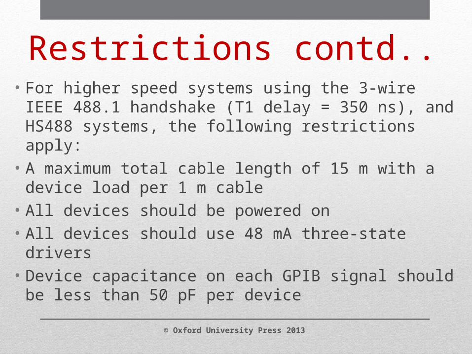
• For higher speed systems using the 3-wire IEEE 488.1 handshake (T1 delay = 350 ns), and HS488 systems, the following restrictions apply:
• A maximum total cable length of 15 m with a device load per 1 m cable
• All devices should be powered on • All devices should use 48 mA three-state drivers • Device capacitance on each GPIB signal should be less than
50 pF per device
Restrictions contd..
© Oxford University Press 2013
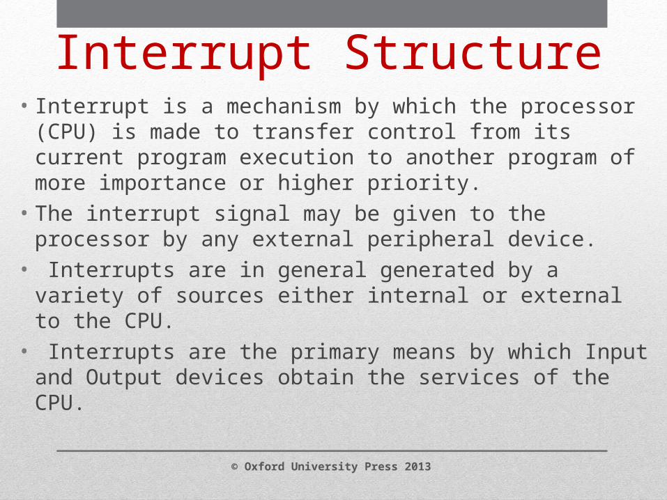
• Interrupt is a mechanism by which the processor (CPU) is made to transfer control from its current program execution to another program of more importance or higher priority.
• The interrupt signal may be given to the processor by any external peripheral device.
• Interrupts are in general generated by a variety of sources either internal or external to the CPU.
• Interrupts are the primary means by which Input and Output devices obtain the services of the CPU.
Interrupt Structure
© Oxford University Press 2013
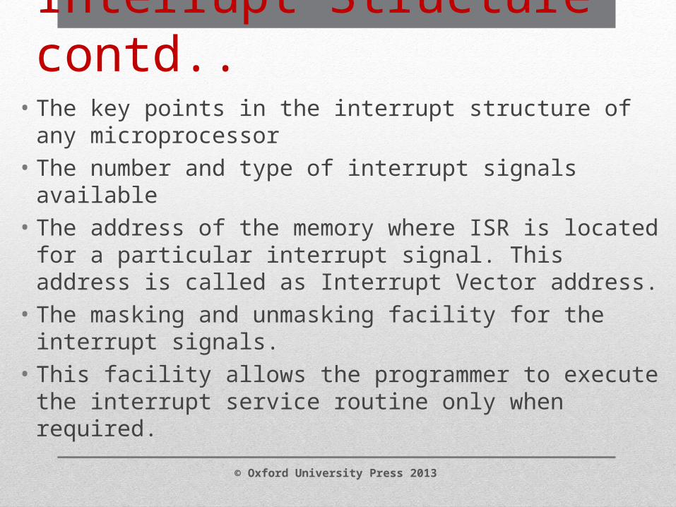
• The key points in the interrupt structure of any microprocessor
• The number and type of interrupt signals available • The address of the memory where ISR is located for a
particular interrupt signal. This address is called as Interrupt Vector address.
• The masking and unmasking facility for the interrupt signals. • This facility allows the programmer to execute the interrupt
service routine only when required.
Interrupt Structure contd..
© Oxford University Press 2013
© Oxford University Press 2013
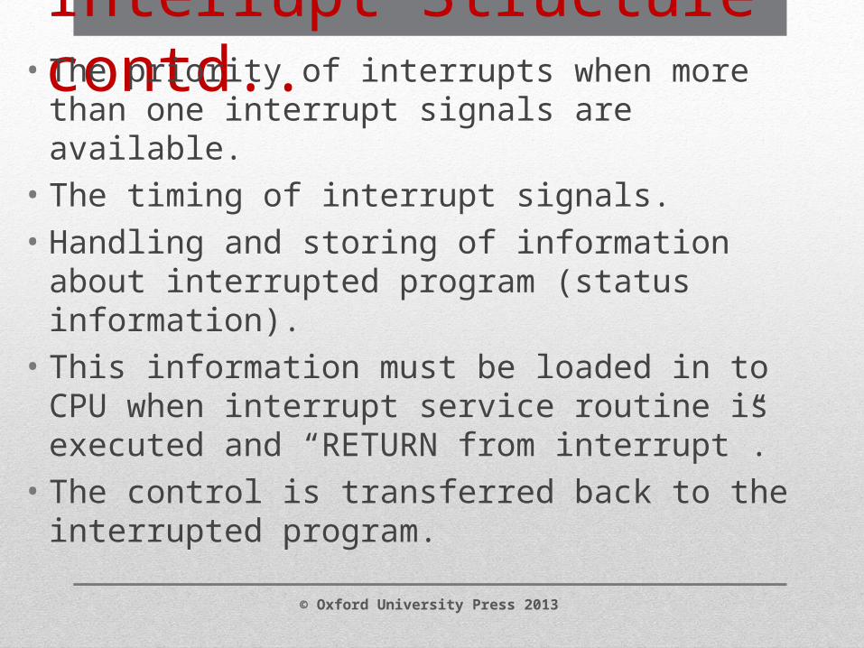
Interrupt Structure contd..• The priority of interrupts when more than one interrupt
signals are available.• The timing of interrupt signals.• Handling and storing of information about interrupted
program (status information). • This information must be loaded in to CPU when interrupt
service routine is executed and “RETURN from interrupt”. • The control is transferred back to the interrupted program.
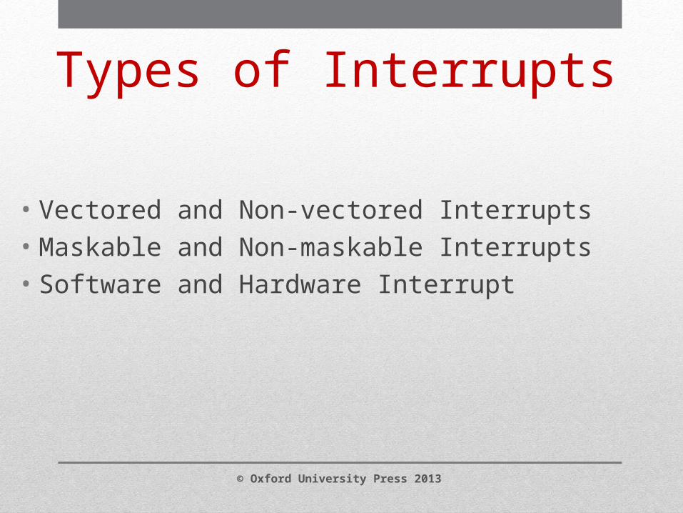
• Vectored and Non-vectored Interrupts• Maskable and Non-maskable Interrupts• Software and Hardware Interrupt
Types of Interrupts
© Oxford University Press 2013
• The Processor will have to store the information about the current program when an interrupt signal is recognized before executing the ISR.
• The processor checks for the Interrupt request signals at the end of every instruction execution.
• If the interrupt is masked, then the interrupt will not be recognized until interrupts are re-enabled.
• The sequence of operations that take place when an interrupt signal is recognized is as followed.
• The CPU responds to an interrupt request by a transfer of control to another program in a manner similar to a subroutine call.
Interrupt Handling Procedure
© Oxford University Press 2013
• Save the PC (Program Counter) contents (address of the next instruction) and supplementary information about current state (flags, registers, etc.) to the stack.
• Load PC with the beginning address of an Interrupt Service Routine (ISR) and start to execute it
• Finish ISR when return instruction is executed• Return to the interrupted program, exactly to the same
point from which it left.
Interrupt Handling Procedure contd..
© Oxford University Press 2013
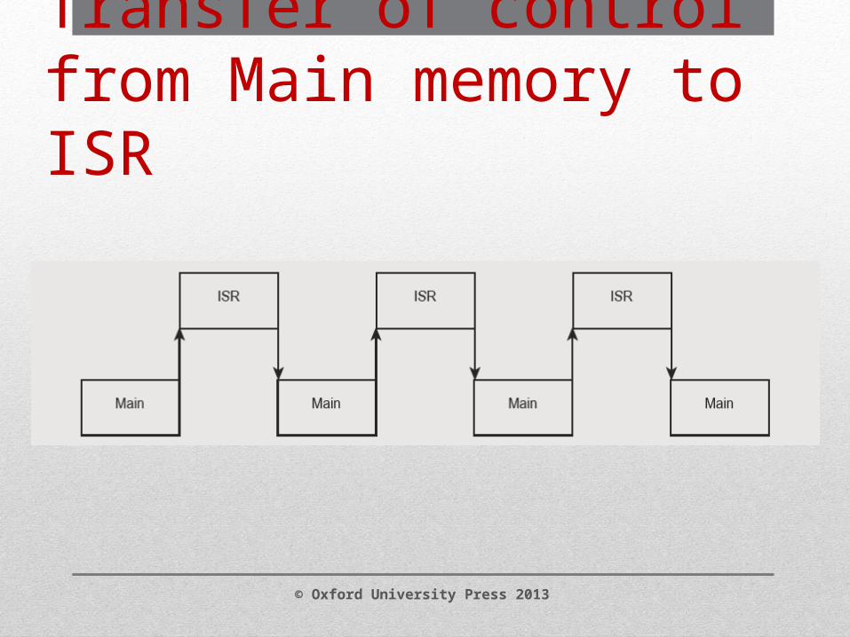
Transfer of control from Main memory to ISR
© Oxford University Press 2013
• Stack is a special memory organization that operates on the principle “Last in First Out” (LIFO) principle.
• The data stored recently will be retrieved first. • Similarly data stored first in the stack can be read last. Stack is a
temporarily storing memory in the RAM area.
Interrupts and Stack memory
© Oxford University Press 2013
© Oxford University Press 2013
Interrupts and Stack memory
• Stack is basically administered by a special register called Stack Pointer (SP).
• SP register always contains the address of the Top of the Stack (ToS).
• Storing a data in stack memory pointed by stack pointer is called PUSH operation.
• Reading a data from the stack is called as POP operation.
• The stack can be accessed by the instructions PUSH and POP.
• The interrupt service routines should not disturb the return address stored by the processor into the stack.
• So, the interrupt service routines should have equal number of PUSH and POP instructions.
• This condition will ensure that the return address stored in the stack is retrieved properly by the processor.
Interrupts and Stack memory contd..
© Oxford University Press 2013
• Intel 8085 has the facility for both software and hardware interrupts.
• The software interrupts are in the form of instructions and the hardware interrupts are applied as signals from the external devices.
Interrupt Sources and their Vector Addresses in 8085
© Oxford University Press 2013
• Intel 8085 has 5 hardware interrupts: INTR, RT 5.5, RST 6.6, RST 7.5, and TRAP.
• The details of the five interrupts are given in the table 5.5. Five pins of 8085 are reserved for the five hardware interrupts.
• All the five interrupts are active high signals. • This means that in order to apply an interrupt, logic 1 or high
level signal should be applied at these pins. • The processor checks the voltage on these pins after the
execution of every instruction.
Hardware Interrupts and Priorities
© Oxford University Press 2013
• If the signal level on any of these 5 pins is at logic 1 and the corresponding interrupt is not masked, then the processor will suspend the current program and execute the corresponding interrupt service routine.
• RST 7.5 interrupt alone is edge triggered. • That means a logic 0 to 1 transition will be treated as an interrupt
input on this line. • The rising edge interrupt can be applied at any time and this will set
a flip flop inside the processor. • The processor will check this flip flop while checking the signal level
on other hardware interrupts.
Hardware Interrupts and Priorities contd..
© Oxford University Press 2013
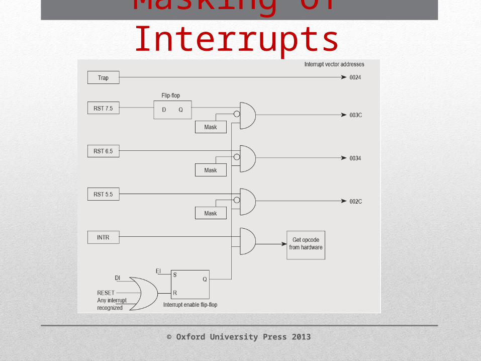
Masking of Interrupts
© Oxford University Press 2013
• The maskable interrupts are by default masked by the RESET signal. So, any interrupt will not be recognized by the hardware reset.
• The interrupts can be enabled by the execution of the instruction, EI – Enable interrupts. This is a must after reset to enable the interrupts.
• The three RST interrupts can be selectively masked by having proper word in Accumulator and executing the SIM (Set Interrupt Mask) instruction. This is called software masking.
Masking of Interrupts contd..
© Oxford University Press 2013
• All the maskable interrupts are disabled whenever an interrupt is recognized.
• So, it is necessary to execute EI instruction every time the interrupts are recognized and serviced by the processor.
• All the maskable interrupts can be disabled by executing an instruction DI – Disable Interrupts. This instruction will reset an interrupt enable flip flop in the processor and the interrupts will be disabled.
• To enable interrupts, EI instruction has to be executed.
© Oxford University Press 2013
Masking of Interrupts contd..
• The SIM instruction is used to mask or unmask the restart RST hardware interrupts.
• The SIM instruction when executed will read the contents of the accumulator and based on that will mask or unmask the interrupts.
• So, SIM instruction must be executed after storing having proper control word in accumulator.
• The format of the control word to be stored in accumulator before executing SIM instruction
SIM Instruction
© Oxford University Press 2013
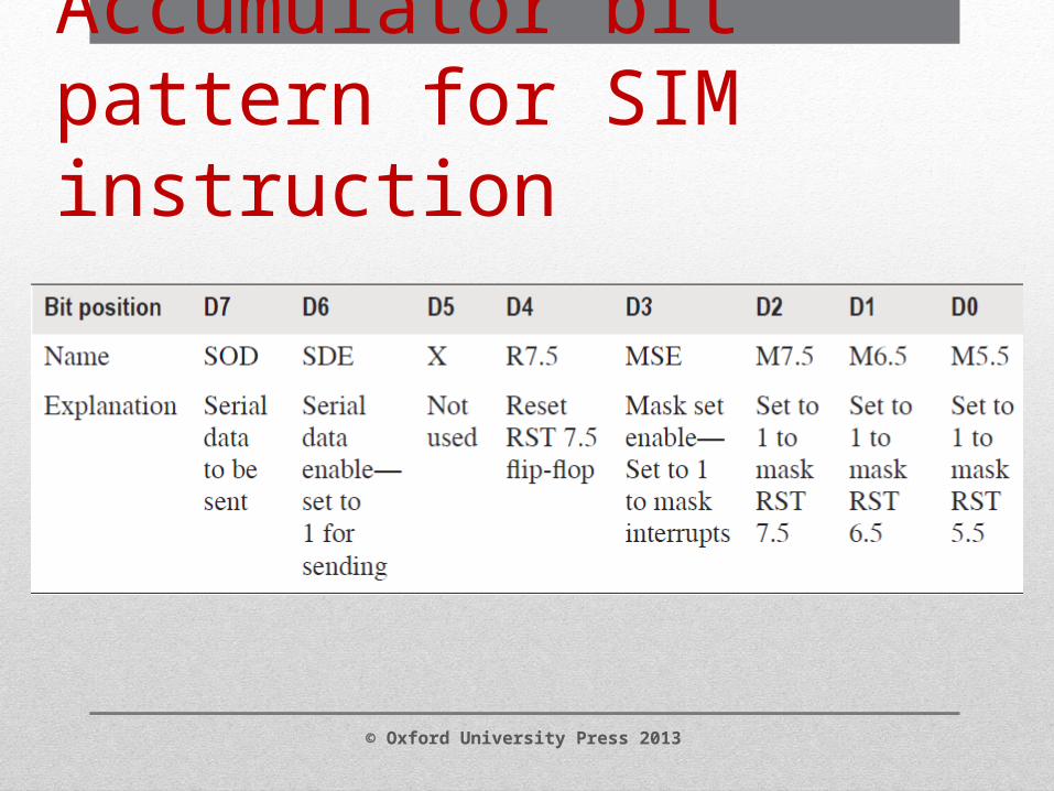
Accumulator bit pattern for SIM instruction
© Oxford University Press 2013
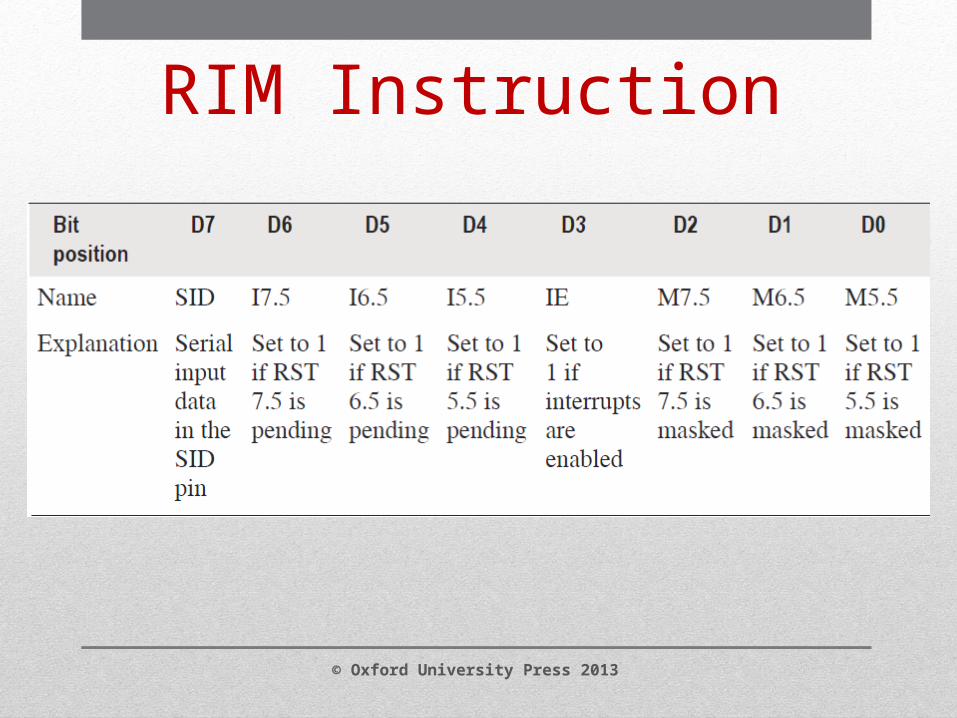
RIM Instruction
© Oxford University Press 2013
• The interrupts are sensed by the processor one cycle before the end of execution of each instruction.
• An interrupt signal must be applied for the proper duration so that it can be recognized. The longest instruction of 8085 takes 18 clock periods.
• So, the interrupt signal must be applied for at least 17.5 clock periods.
• This decides the minimum pulse width for the interrupt signals.
Timing of Interrupts
© Oxford University Press 2013
• Any other interrupt issued to the microprocessor will be recognized once EI instruction is executed.
• If, the programmer has written the EI instruction at the start of the interrupt service routine, then the microprocessor can be interrupted once again before the completion of the interrupt service routine.
© Oxford University Press 2013
Timing of Interrupts
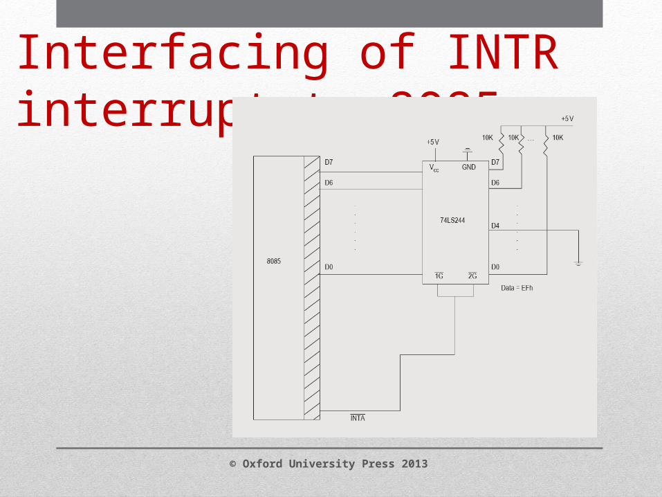
Interfacing of INTR interrupt to 8085
© Oxford University Press 2013
• Different data transfer schemes are available for data transfer between two processors or between a processor and I/O device.
• The different data transfer schemes are programmed data transfer and DMA method, polled method and interrupt driven method, serial and parallel data transfer schemes.
• The various serial port standards such as RS232, RS485, IEEE488 and GPIB are used for data transfer in different applications.
• Interrupts are an important mechanism available in the processors to temporarily stop current program execution and execute a program of higher priority.
Summary
© Oxford University Press 2013
• The source of interrupts, interrupt vector addresses, priorities, and timing of interrupts are very important to program and understand the operation of Interrupt mechanism in a processor.
• The interrupts can be either hardware generated and can be random, or the software generated and can be programmed.
• It has to be noted that the processor can be interrupted before the completion of an interrupt service routine if the program has executed the instruction EI. This enables nested interrupt service routine execution.
© Oxford University Press 2013
Summary
Related Documents