www.binils.com for Anna University | Polytechnic and schools Download Binils Android App in Playstore Download Photoplex App 3.2 PARALLEL COMMUNICATION INTERFACE 8255 (PROGRAMMABLE PERIPHERAL INTERFACE) The 8255 is a widely used, programmable parallel I/O device. It can be programmed to transfer data under data under various conditions, from simple I/O to interrupt I/O. It is an important general purpose I/O device that can be used with almost any microprocessor. The 8255 has 24 I/O pins that can be grouped primarily into two 8 bit parallel ports: A and B, with the remaining 8 bits as Port C. The 8 bits of port C can be used as individual bits or be grouped into two 4 bit ports: Cupper (CU) and Cower (CL). The functions of these ports are defined by writing a control word in the control register. 8255 can be used in two modes: Bit set/Reset (BSR) mode and I/O mode. The BSR mode is used to set or reset the bits in port C. The I/O mode is further divided into 3 modes: mode 0- all ports function as simple I/O ports mode 1 - a handshake mode whereby Port A and/or Port B use bits from Port CA’s handshake signals mode 2- Port A can be set up for bidirectional data transfer using handshake signals from Port C, and Port B can be set up either in mode 0 or mode 1

Welcome message from author
This document is posted to help you gain knowledge. Please leave a comment to let me know what you think about it! Share it to your friends and learn new things together.
Transcript

www.binils.com for Anna University | Polytechnic and schools
Download Binils Android App in Playstore Download Photoplex App
3.2 PARALLEL COMMUNICATION INTERFACE
8255 (PROGRAMMABLE PERIPHERAL INTERFACE)
The 8255 is a widely used, programmable parallel I/O device. It can be programmed to
transfer data under data under various conditions, from simple I/O to interrupt I/O. It is an
important general purpose I/O device that can be used with almost any microprocessor.
The 8255 has 24 I/O pins that can be grouped primarily into two 8 bit parallel ports: A
and B, with the remaining 8 bits as Port C. The 8 bits of port C can be used as individual bits
or be grouped into two 4 bit ports: Cupper (CU) and Cower (CL). The functions of these ports
are defined by writing a control word in the control register.
8255 can be used in two modes: Bit set/Reset (BSR) mode and I/O mode.
The BSR mode is used to set or reset the bits in port C.
The I/O mode is further divided into 3 modes:
mode 0- all ports function as simple I/O ports
mode 1 - a handshake mode whereby Port A and/or Port B use bits
from Port CA’s handshake signals
mode 2- Port A can be set up for bidirectional data transfer using
handshake signals from Port C, and Port B can be set up either in
mode 0 or mode 1

www.binils.com for Anna University | Polytechnic and schools
Download Binils Android App in Playstore Download Photoplex App
Figure 3.2.1 Pin Configuration of 8255
[Source: Advanced Microprocessors and Microcontrollers by A.K Ray & K.M.Bhu`rchandi]
The signal description of 8255 is briefly presented as follows:
PA7-PA0: These are eight port A lines that acts as either latched output or
buffered input lines depending upon the control word loaded into the control
word register.
PC7-PC4: Upper nibble of port C lines. They may act as either output latches or
input buffers lines. This port also can be used for generation of handshake lines
in mode 1 or mode 2.
PC3-PC0: These are the lower port C lines, other details are the same as PC7-
PC4 lines.
PB0-PB7: These are the eight port B lines which are used as latched output lines
or buffered input lines in the same way as port A.
RD: This is the input line driven by the microprocessor and should be low to
indicate read operation to8255.
WR: This is an input line driven by the microprocessor. A low on this line indicates write
operation.
CS: This is a chip select line. If this line goes low, it enables the 8255 to respond

www.binils.com for Anna University | Polytechnic and schools
Download Binils Android App in Playstore Download Photoplex App
to RD and WR signals, otherwise RD and WR signal are neglected.
A1-A0: These are the address input lines and are driven by the microprocessor.
These lines A1-A0 with RD, WR and CS from the following operations for
8255. In case of 8086 systems, if the 8255 is to be interfaced with lower order
data bus, the A0 and A1 pins of 8255 are connected with A1 and A2
respectively.
D0-D7: These are the data bus lines those carry data or control word to/from the
microprocessor.
RESET: A logic high on this line clears the control word register of 8255. All
ports are set as input ports by default after reset.
8255 BLOCK DIAGRAM:
Figure 3.2.2 Block Diagram of 8255
[Source: Advanced Microprocessors and Microcontrollers by A.K Ray & K.M.Bhurchandi]
Data Bus Buffer-This three-state bi-directional 8-bit buffer is used to interface
the 8255 to the system data bus. Data is transmitted or received by the buffer

www.binils.com for Anna University | Polytechnic and schools
Download Binils Android App in Playstore Download Photoplex App
upon execution of input or output instructions byte CPU. Control words and
status information are also transferred through the data bus buffer.
Read/Write and Control Logic
The function of this block is to manage all of the internal and external transfers
of both Data and Control or Status words. It accepts inputs from the CPU Address and
Control busses and in turn, issues commands to both of the Control Groups.A0 and A1
Port Select 0 and Port Select 1. These input signals, in conjunction with the RD and WR
inputs, control the selection of one of the three ports or the control word register as shown
in Table 3.2.1.They are normally connected to the least significant bits of the address
bus (A0 and A1).
CS A1 A0 Selection
0 0 0 Port A
0 0 1 Port B
0 1 0 Port C
0 1 1 Control
Register
1 x x 8255 is not
selected
Table 3.2.1 Port / Control Register Selection
[Source: Advanced Microprocessors and Microcontrollers by A.K Ray & K.M.Bhurchandi]
Group A and Group B Controls
The functional configuration of each port is programmed by the systems
software. Each of the Control blocks (Group A and Group B) accepts
"commands" from the Read/Write Control logic, receives "control words"
from the internal data bus and issues the proper commands to its associated
ports.
Ports A, B, and C
The 8255 contains three 8-bit ports (A, B, and C). All can be configured to a
wide variety of functional characteristics by the system software but each has its own
special features or "personality" to further enhance the power and flexibility of the 8255.

www.binils.com for Anna University | Polytechnic and schools
Download Binils Android App in Playstore Download Photoplex App
Port A One 8-bit data output latch/buffer and one 8-bit data input latch. Both "pull-up"
And "pull-down" bus-hold devices are present on Port A.
Port B One 8-bit data input/output latch/buffer and one 8-bit data input buffer.
Port C One 8-bit data output latch/buffer and one 8-bit data input buffer (no latch for
input).
This port can be divided into two 4-bit ports under the mode control. Each 4-bit
port contains a 4-bit latch and it can be used for the control signal output and status signal
inputs in conjunction with ports A and B.
OPERATION MODES OF 8255:
The bit pattern loaded in control word register specifies an I/O function
for each port and the mode of operation in which the ports are to be used.
There are two different control word formats which specify two basic modes:
BSR (Bit set reset) mode
I/O mode
The two basic modes are selected by D7 bit of control register. When D7=1 it is an I/O
mode and when
D7=0; it is a BSR mode.
BSR MODE-
The BSR mode is a port C bit set/reset mode.
The individual bit of port C can be set or reset by writing control word in
the control register.
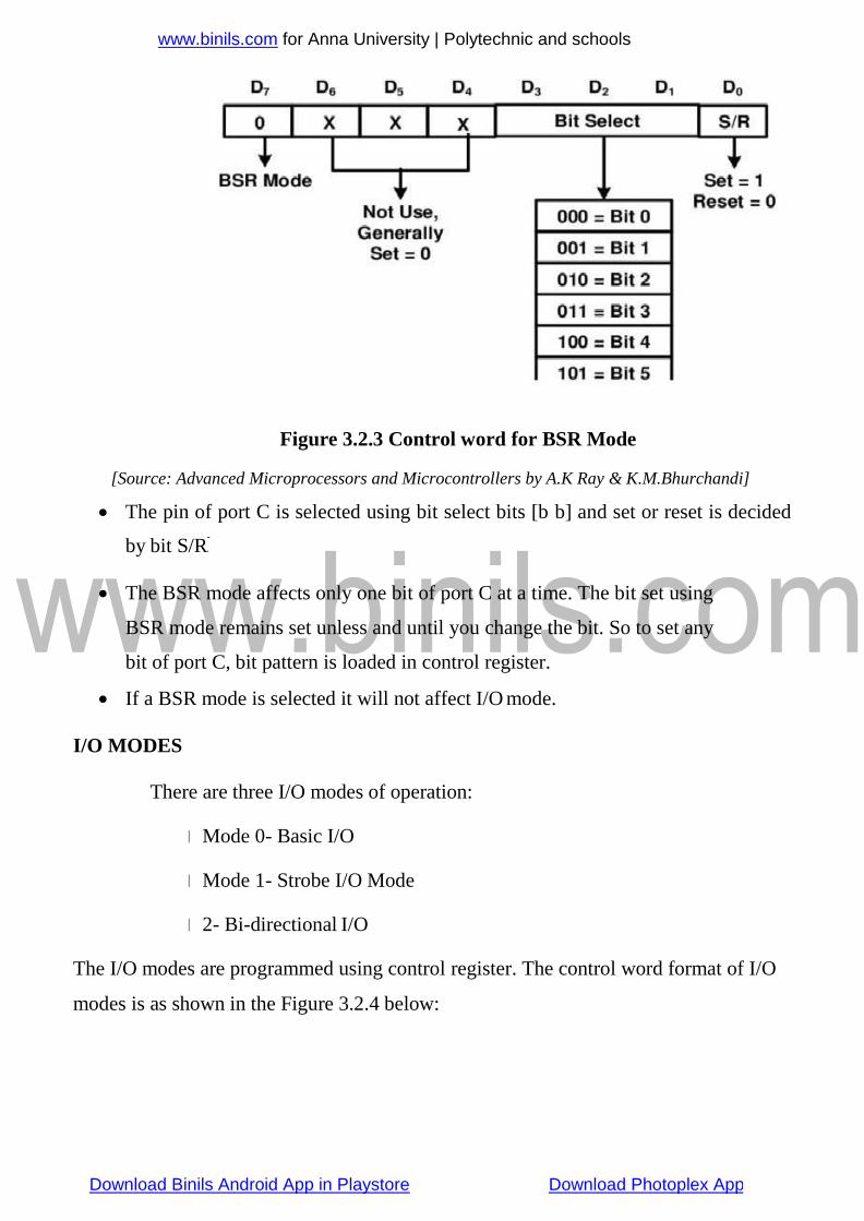
The control word format of BSR mode is as shown in the Figure 3.2.3 below:
.
www.binils.com for Anna University | Polytechnic and schools
Download Binils Android App in Playstore Download Photoplex App
Figure 3.2.3 Control word for BSR Mode
[Source: Advanced Microprocessors and Microcontrollers by A.K Ray & K.M.Bhurchandi]
The pin of port C is selected using bit select bits [b b] and set or reset is decided
by bit S/R. ̅
The BSR mode affects only one bit of port C at a time. The bit set using
BSR mode remains set unless and until you change the bit. So to set any
bit of port C, bit pattern is loaded in control register.
If a BSR mode is selected it will not affect I/O mode.
I/O MODES
There are three I/O modes of operation:
Mode 0- Basic I/O
Mode 1- Strobe I/O Mode
2- Bi-directional I/O
The I/O modes are programmed using control register. The control word format of I/O
modes is as shown in the Figure 3.2.4 below:

www.binils.com for Anna University | Polytechnic and schools
Download Binils Android App in Playstore Download Photoplex App
Figure 3.2.4 Control word for I/O Mode
[Source: Advanced Microprocessors and Microcontrollers by A.K Ray & K.M.Bhurchandi]
Function of each bit is as follows:
1. D7– When the bit D7 = 1 then I/O mode is selected, if D7=0
then BSR mode is selected. The function of bits D0 to D6
is independent on mode (I/O mode or Bermudez).
2. D6 and D5-In I/O mode the bits D6 and D5 specifies the
different I/O modes for group A i.e. Mode 0, Mode 1 and
Mode 2 for port A and port Cupper.
3. D2 – In I/O mode the bit D2 specifies the different I/O modes
for group B i.e. Mode 0 and Mode 1 for port B and port C
lower.
All the 3 modes i.e. Mode 0, Mode 1 and Mode 2 are only for group A
ports, but for group B only 2 modes i.e. Mode 0 and Mode 1 are provided. When
8255 is reset, it will clear control word register contents and all the ports are set
to input mode. The ports of 8255 can be programmed for other modes by

www.binils.com for Anna University | Polytechnic and schools
Download Binils Android App in Playstore Download Photoplex App
Sending appropriate bit pattern to control register.
Mode 0: Simple Input or Output
In this mode, Port A and Port B are used as two simple 8-bit I/O ports
and Port C as two4-bit I/O ports. Each port (or half-port, in case of Port C) can
be programmed to function as simply an input port or an output port. The
input/output features in mode 0 are: Outputs are latched, Inputs are not latched.
Ports do not have handshake or interrupt capability.
Mode 1: Input or Output with handshake
In mode 1, handshake signals are exchanged between the microprocessor
and peripherals prior to data transfer. The ports (A and B) function as 8-bit I/O
ports. They can be configured either as input or output ports. Each port (Port A
and Port B) uses 3 lines from port C as handshake signals. The remaining two
lines of port C can be used for simple I/O functions. Input and output data are
latched and Interrupt logic is supported.
Mode 1: Input control signals
Figure 3.2.5 Input Control Signals
[Source: Advanced Microprocessors and Microcontrollers by A.K Ray & K.M.Bhurchandi]

www.binils.com for Anna University | Polytechnic and schools
STB (Strobe Input): This signal (active low) is generated by a peripheral
device that it has transmitted abyte of data. The 8255, in response to, generates
Download Binils Android App in Playstore Download Photoplex App
IBF and INTR.
IBF (Input buffer full): This signal is an acknowledgement by the 8255 to
indicate that the input latches received the data byte. This is reset when the
microprocessor reads the data.
INTR (Interrupt Request): This is an output signal that may be used to
interrupt the microprocessor. This signal is generated if , IBF and INTE are
all at logic 1.
INTE (Interrupt Enable): This is an internal flip-flop to a port and needs to
be set to generate the INTR signal. The two flip-flops INTEA and INTEB are
set /reset using the BSR mode. The INTEA is enabled or disabled through PC4,
and INTEB is enabled or disabled through PC2.
Figure 3.2.6 shows the Mode 1 strobe Input Data Transfer.
Figure 3.2.6 Mode 1 strobe Input Data Transfer
[Source: Advanced Microprocessors and Microcontrollers by A.K Ray & K.M.Bhurchandi]

www.binils.com for Anna University | Polytechnic and schools
signals from Port C as handshake signals for data transfer. The remaining three
Download Binils Android App in Playstore Download Photoplex App
Figure 3.2.7 Output control signals
[Source: Advanced Microprocessors and Microcontrollers by A.K Ray & K.M.Bhurchandi]
OUTPUT CONTROL SIGNAL DEFINITION:
OBF (Output Buffer Full): This is an output signal that goes low when the
microprocessor writes data into the output latch of the 8255. This signal
indicates to an output peripheral that new data is ready to be read. It goes high
again after the 8255 receives a signal from the peripheral.
ACK (Acknowledge): This is an input signal from a peripheral that must output
a low when the peripheral receives the data from the 8255 ports.
INTR (Interrupt Request): This is an output signal, and it is set by the rising
edge of the signal. This signal can be used to interrupt the microprocessor to
request the next data byte for output. The INTR is setand INTE are all one and
reset by the rising edge of RD signal.
INTEA & INTEB is controlled by bit set/reset of PC6 & PC2 respectively.
Mode 2: Bidirectional Data Transfer
This mode is used primarily in applications such as data transfer between
the two computers or floppy disk controller interface. Port A can be configured

www.binils.com for Anna University | Polytechnic and schools
3.3 SERIAL COMMUNICATION INTERFACE
Download Binils Android App in Playstore Download Photoplex App
PROGRAMMABLE COMMUINCATION INTERFACE (INTEL 8251A)
The 8251 is a programmable chip designed for synchronous and asynchronous serial
data communication .USART (Universal Synchronous/Asynchronous Receiver/Transmitter)
is the key component for converting parallel data to serial form and vice versa two types of
serial data communications are widely used -Asynchronous Communication and
synchronous Communication.
Figure 3.3.1 Block diagram of 8251
[Source: Advanced Microprocessors and Microcontrollers by A.K Ray & K.M.Bhurchandi]

www.binils.com for Anna University | Polytechnic and schools
SIGNAL DESCRIPTION OF 8251
Download Binils Android App in Playstore Download Photoplex App
D 0 to D 7 (l/O)
This is bidirectional data bus which receives control words and transmits
data from the CPU and sends status words and received data to CPU.
RESET (Input)
A "High" on this input forces the 8251 into "reset status." The device
waits for the writing of "mode instruction." The min. reset width is six clock
inputs during the operating status of CLK.
CLK (Input)
CLK signal is used to generate internal device timing. CLK signal is
independent of RXC or TXC. However, the frequency of CLK must be greater
than 30 times the RXC and TXC at Synchronous mode and Asynchronous "x1"
mode, and must be greater than 5 times at Asynchronous "x16" and "x64" mode.
WR (Input)
This is the "active low" input terminal which receives a signal for writing
transmit data and control words from the CPU into the 8251.
RD (Input)
This is the "active low" input terminal which receives a signal for reading receive
data and status words from the 8251.
C/D (Input)
This is an input terminal which receives a signal for selecting data or
command words and status words when the 8251 is accessed by the CPU. If
C/D = low, data will be accessed. If C/D = high, command word or status
word will beaccessed.

www.binils.com for Anna University | Polytechnic and schools
CS (Input)
Download Binils Android App in Playstore Download Photoplex App
This is the "active low" input terminal which selects the 8251 at low
level when the CPU accesses.
TXD (output)
This is an output terminal for transmitting data from which serial-
converted data is sent out. The device is in "mark status" (high level) after
resetting or during a status when transmit is disabled. It is also possible to set
the device in "break status" (low level) by a command.
TXRDY (output)
This is an output terminal which indicates that the 8251is ready to accept
a transmitted data character. Butte terminal is always at low level if CTS =
high or the device was set in "TX disable status" by a command. Note: TXRDY
status word indicates that transmit data character is receivable, regardless of
CTS or command. If the CPU writes a data character, TXRDY will be reset by
the leading edge or WR signal.
TXEMPTY (Output)
This is an output terminal which indicates that the 8251 has transmitted
all the characters and had no data character. In "synchronous mode," the
terminal is at high level, if transmit data characters are no longer remaining and
sync characters are automatically transmitted. If the CPU writes a data
character, TXEMPTY will be reset by the leading edge of WR signal.
TXC (Input)
This is a clock input signal which determines the transfer speed of
transmitted data. In "synchronous mode," the baud rate will be the same as the
frequency of TXC. In "asynchronous mode", it is possible to select the baud rate
www.binils.com for Anna University | Polytechnic and schools
factor by mode instruction. It can be 1, 1/16 or 1/64 the TXC. The falling edge
Download Binils Android App in Playstore Download Photoplex App
of TXC sifts the serial data out of the8251.
RXD (input)
This is a terminal which receives serial data.
RXRDY (Output)
This is a terminal which indicates that the 8251 contains a character that
is ready to READ. If the CPU reads a data character, RXRDY will be reset by
the leading edge of RD signal. Unless the CPU reads a data character before the
next one is received completely, the preceding data will be lost. In such a case,
an overrun error flag status word will be set.
RXC (Input)
This is a clock input signal which determines the transfer speed of
received data. In "synchronous mode," the baud rate is the same as the
frequency of RXC. In "asynchronous mode," it is possible to select the baud
rate factor by mode instruction. It can be 1, 1/16, 1/64 the RXC.
SYNDET/BD (Input or output)
This is a terminal whose function changes according to mode. In "internal
synchronous mode." this terminal is at high level, if sync characters are received
and synchronized. If a status word is read, the terminal will be reset. In "external
synchronous mode, "this is an input terminal. A "High" on this input forces the
8251 to start receiving data characters.
In "asynchronous mode," this is an output terminal which generates "high
level"output upon the detection of a "break" character if receiver data contains
a "low-level" space between the stop bits of two continuous characters. The
terminal will be reset, if RXD is at high level. After Reset is active, the terminal
will be output at low level.

www.binils.com for Anna University | Polytechnic and schools
DSR (Input)
Download Binils Android App in Playstore Download Photoplex App
This is an input port for MODEM interface. The input status of the
terminal can be recognized by the C PU reading status words.
DTR (Output)
This is an output port for MODEM interface. It is possible to set the status of DTR
by a command.
CTS (Input)
This is an input terminal for MODEM interface which is used for
controlling a transmit circuit. The terminal controls data transmission if the
device is set in "TX Enable" status by a command. Data is transmittable if the
terminal is at low level.
RTS (Output)
This is an output port for MODEM interface. It is possible to set the status RTS by
a command.
CONTROL WORDS
There are two types of control word.
1. Mode instruction (setting of function)
2. Command (setting of operation)
MODE INSTRUCTION
Mode instruction is used for setting the function of the 8251. Mode
instruction will be in "wait for write" at either internal reset or external reset.
That is, the writing of a control word after resetting will be recognized as a
"mode instruction."
Items set by mode instruction are as follows:
• Synchronous/asynchronous mode

www.binils.com for Anna University | Polytechnic and schools
Download Binils Android App in Playstore Download Photoplex App
• Stop bit length (asynchronous mode)
• Character length
• Parity bit
• Baud rate factor (asynchronous mode)
• Internal/external synchronization (synchronous mode)
• Number of synchronous characters (Synchronous mode)
The bit configuration of mode instruction is shown in Figure 3.3.2. In the case
of synchronous mode, it’s necessary to write one-or two byte sync characters.
If sync characters were written, a function will be set because the writing of
sync characters constitutes part of mode instruction.
Figure 3.3.2 Mode instruction format-Sync
[Source: Advanced Microprocessors and Microcontrollers by A.K Ray & K.M.Bhurchandi]
COMMAND
Command is used for setting the operation of the 8251. It is possible to
write a command whenever necessary after writing a mode instruction and
sync characters. Items to be set by command are as follows:
• Transmit Enable/Disable

www.binils.com for Anna University | Polytechnic and schools
Download Binils Android App in Playstore Download Photoplex App ``````
• Receive Enable/Disable
• DTR, RTS Output of data.
• Resetting of error flag.
• Sending to break characters
• Internal resetting
• Hunt mode (synchronous mode)
The bit configuration of Command instruction is shown in Figure 3.3.3.
Figure 3.3.3 Command word
[Source: Advanced Microprocessors and Microcontrollers by A.K Ray & K.M.Bhurchandi]
Status Word
It is possible to see the internal status of the 8251 by reading a status
word. The bit configuration of status word is shown in Figure 3.3.4.

www.binils.com for Anna University | Polytechnic and schools
Download Binils Android App in Playstore Download Photoplex App ``````
Figure 3.3.4 status word
[Source: Advanced Microprocessors and Microcontrollers by A.K Ray & K.M.Bhurchandi]

www.binils.com for Anna University | Polytechnic and schools
Download Binils Android App in Playstore Download Photoplex App
3.5 TIMER
PROGRAMMABLE INTERVAL TIMER (8253/8254)
The Intel 8253 and 8254 are Programmable Interval Timers (PTIs)
designed for microprocessors to perform timing and counting functions using
three 16-bit registers. Each counter has 2 input pins, i.e. Clock & Gate, and 1
pin for “OUT” output. To operate a counter, a 16-bit count is loaded in its
register.On command, it begins to decrement the count until it reaches 0, then
it generates a pulse that can be used to interrupt the CPU.
Difference between 8253 and 8254
825
3
825
4
Its operating frequency is 0 - 2.6 MHz Its operating frequency is 0 - 10 MHz
It uses N-MOS technology It uses H-MOS technology
Read-Back command is not available Read-Back command is available
Reads and writes of the same counter
cannot be
Interleaved.
Reads and writes of the same counter
can be
Interleaved.

www.binils.com for Anna University | Polytechnic and schools
Download Binils Android App in Playstore Download Photoplex App
Figure 3.5.1 Internal blocks of 8253 and pin diagram
[Source: Advanced Microprocessors and Microcontrollers by A.K Ray & K.M.Bhurchandi]
CS - Chip select .When it is low, enables the communication between CPU and 8253.
WR-When it is low, the CPU output data in the form of mode information are loading
counters.
RD – When it is low, the CPU reads data.
A0-A1: These pins are connected to address bus. These are used to select one of the three
counters.
D0-D7: These are tri-state bidirectional data bus used to interface 8253 to the system data
bus.
CLK0, CLK1and CLK2-
These are clock signals for counter0, counter1 and counter2.
GATE0, GATE1 and GATE2-
These are gate terminals for counter0, counter1 and counter2.
OUT0, OUT1and OUT2-
These are output terminals for counter0, counter1 and counter2.
In the above Figure 3.5.1, there are three counters, a data bus buffer,

www.binils.com for Anna University | Polytechnic and schools
Download Binils Android App in Playstore Download Photoplex App
Read/Write control logic, and a control register. Each counter has two input
signals - CLOCK & GATE and one output signal - OUT.
Data Bus Buffer
It is a tri-state, bi-directional, 8-bit buffer, which is used to interface the
8253/54 to the system data bus. It has three basic functions
Programming the modes of 8253/54.
Loading the count registers.
Reading the count values.
Read/Write Logic
It includes 5 signals, i.e. RD, WR, CS and the address lines A0 & A1. In
the peripheral I/O mode, the RD and WR signals are connected to IOR and
IOW, respectively. In the memory mapped I/O mode, these are connected to
MEMR and MEMW.
Address lines A0 & A1 of the CPU are connected to lines A0 and A1 of
the 8253/54, and CS is tied to decoded address. The control word register and
counters are selected according to the signals on lines A0 & A1.
A1 A0 Selection
0 0 Counter 0
0 1 Counter 1
1 0 Counter 2
1 1 Control Word
Register
X X No Selection
Table 3.5.1 Selection of Counters
[Source: Advanced Microprocessors and Microcontrollers by A.K Ray & K.M.Bhurchandi]

www.binils.com for Anna University | Polytechnic and schools
COUNTERS
Download Binils Android App in Playstore Download Photoplex App
Each counter consists of a single, 16 bit-down counter, which can be
operated in either binary or BCD. Its input and output is configured by the
selection of modes stored in the control word register. The programmer can
read the contents of any of the three counters without disturbing the actual
count in process.
Control Word Register:
The bits D7 and D6 of the control word are to select one of the 3 counters.D5 and D4 are
for loading /reading the count.D3, D2 and D1 are for the selection of operating mode of
the selected counter.
Figure 3.5.2 Control Word format of 8253
[Source: Advanced Microprocessors and Microcontrollers by A.K Ray & K.M.Bhurchandi]

www.binils.com for Anna University | Polytechnic and schools
Download Binils Android App in Playstore Download Photoplex App
OPERATION OF 8253:
The functions of the 8253/54 can be described by Write and Read operation.
WRITE Operation:
Write a control word into control register.
Load the low-order byte of a count in the counter register.
Load the high-order byte of count in the counter register.
READ OPERATION:
1. Simple Read: It involves reading a count after inhibiting the counter by
controlling the gate input or the clock input of the selected counter, and two
I/O read operations are performed by the CPU. The first I/O operation reads
the low-order byte, and the second I/O operation reads the high order byte.
2. Counter Latch Command: In the second method, an appropriate control
word is written into the control register to latch a count in the output latch, and
two I/O read operations are performed byte CPU. The first I/O operation
reads the low-order byte, and the second I/O operation reads the high order
byte.
3. Read-Back Command (Available only for 8254): The third method
uses the Read-Back command. This command allows the user to check the
count value, programmed Mode, and current status of the OUT pin and Null
count flag of the selected counter(s).
8254 MODES OF OPERATION:
1. Mode 0 (Interrupt on terminal count)
2. Mode 1 (programmable Moonshot)
3. Mode 2 (Rate Generator)
4.Mode 3 (Square Wave Generator)
5. Mode4(Software Triggered Strobe)
www.binils.com for Anna University | Polytechnic and schools
Download Binils Android App in Playstore Download Photoplex App
`
6. Mode 5 (Hardware Triggered Strobe)
The Description and operation of various modes of timer are depicted in the figures
below. [Figure 3.5.3(a) to Figure 3.5.3(f)]
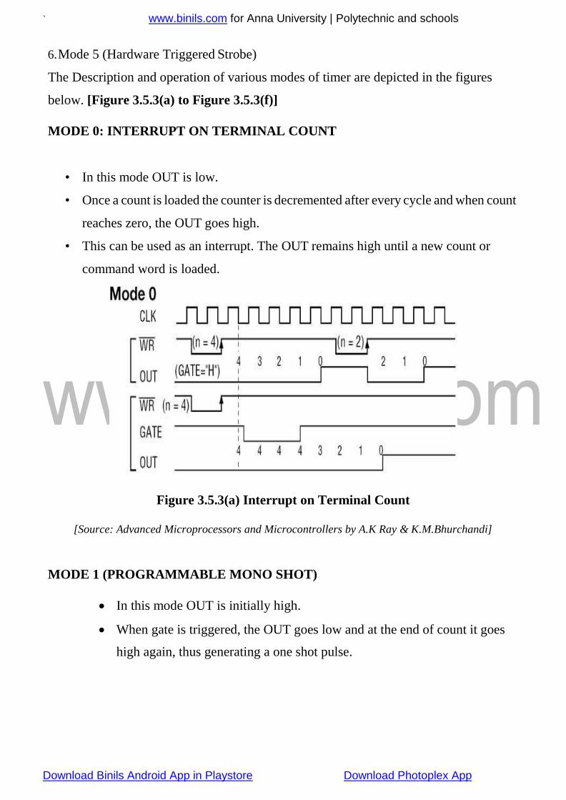
MODE 0: INTERRUPT ON TERMINAL COUNT
• In this mode OUT is low.
• Once a count is loaded the counter is decremented after every cycle and when count
reaches zero, the OUT goes high.
• This can be used as an interrupt. The OUT remains high until a new count or
command word is loaded.
Figure 3.5.3(a) Interrupt on Terminal Count
[Source: Advanced Microprocessors and Microcontrollers by A.K Ray & K.M.Bhurchandi]
MODE 1 (PROGRAMMABLE MONO SHOT)
In this mode OUT is initially high.
When gate is triggered, the OUT goes low and at the end of count it goes
high again, thus generating a one shot pulse.

www.binils.com for Anna University | Polytechnic and schools
Download Binils Android App in Playstore Download Photoplex App
`
Figure 3.5.3(b) Programmable Mono Shot
[Source: Advanced Microprocessors and Microcontrollers by A.K Ray & K.M.Bhurchandi]
MODE 2 (RATE GENERATOR)
The mode is used to generate a pulse equal to given clock period at a given interval.
When a count is loaded, the OUT stays high until count reaches 1 and then OUT
goes low for 1 clock period then gets reloaded automatically and this is how pulse
gets generated continuously.
Figure 3.5.3(c) Rate Generator
[Source: Advanced Microprocessors and Microcontrollers by A.K Ray & K.M.Bhurchandi]

www.binils.com for Anna University | Polytechnic and schools
Download Binils Android App in Playstore Download Photoplex App
`
MODE 3 (SQUARE WAVE GENERATOR)
• In this a continuous square wave with period equal to count is generated.
• The frequency of square wave = frequency of clock divide by count.
• if count (N) is odd pulse stay high for (N + 1)/2 and low for (N - 1)/2
Figure 3.5.3(d) Square Wave Generator
[Source: Advanced Microprocessors and Microcontrollers by A.K Ray & K.M.Bhurchandi]
Mode 4 (Software Triggered Strobe)
In this mode OUT is initially high; it
goes low for one clock period at the
end of count.
The count must be reloaded for subsequent outputs.

www.binils.com for Anna University | Polytechnic and schools
Download Binils Android App in Playstore Download Photoplex App
`
Figure 3.5.3(e) Software Triggered Strobe
[Source: Advanced Microprocessors and Microcontrollers by A.K Ray & K.M.Bhurchandi]
Mode 5 (hardware triggered strobe)
• Same as MODE4 except that it is triggered by rising pulse at gate.
Figure 3.5.3(f) Hardware Triggered Strobe
[Source: Advanced Microprocessors and Microcontrollers by A.K Ray & K.M.Bhurchandi]

`
www.binils.com for Anna University | Polytechnic and schools
Download Binils Android App in Playstore Download Photoplex App
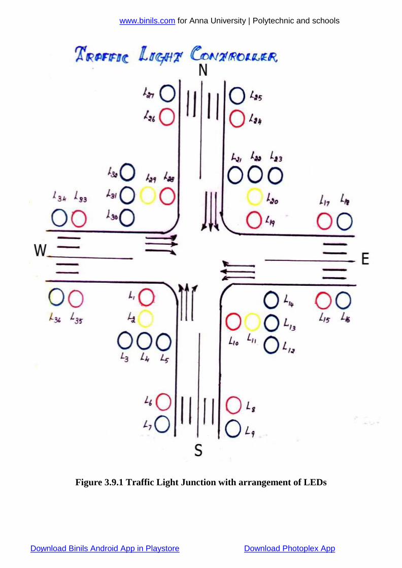
3.9 TRAFFIC LIGHT CONTROLLER
Traffic light controller interface module is designed to simulate the function of
four way traffic light controller. Combinations of red, amber and green LEDs are
provided to indicate Halt, Wait and Go signals for vehicles. Combination of red and
green LEDs are provided for pedestrian crossing.36 LEDs are arranged in the form of an
intersection.
A typical junction
Is represented in the Figure 3.9.1. At the left corner of each road, a group of five LEDs
(red, amber and 3 green) are arranged in the form of a T-section to control the traffic of
that road. Each road is named North (N), South(S), East (E) and West (W).
LED’s L1, L10, L19& L28 (Red) are for the stop signal for the vehicles on the
L2, L11, L20 & L29 (Amber) indicates wait state for vehicles on the Road N, S,
W, & E respectively.
L3, L4 & L5 (Green) are for left, strait and right turn for the vehicles on road S.
Similarly, L12-L13-L14, L23-L22-L21 & L32-L31-L30 simulates same function
for the roads E, N, W respectively.
A total of 16 LED’s (2 Red & 2 Green at each road) are provided for pedestrian
crossing. L7-L9. L16-L18, L25-L27 & L34-L36 (Green) when ON allows
pedestrians to cross and L6- L8, L15-L17, L24-L26 & L33-L35 (Red) when ON
alarms the pedestrians to wait.
To minimize the hardware pedestrian’s indicator LEDs (both red and green are
connected to same port lines (PC4 to PC7) with red inverted.

`
www.binils.com for Anna University | Polytechnic and schools
Download Binils Android App in Playstore Download Photoplex App
Red LEDs L10 & L 28 are connected to port lines PC2 & PC3 while L1 & L19
are connected to lines PC0 & PC1 after inversion. All other LED’s (amber and
green) are connected to port A & B.
WORKING:
8255 is interfaced with 8086 in I/O mapped I/O and all ports are output ports. The basic
operation of the interface is explained with the help of the enclosed program. The
enclosed program assumes no entry of vehicles from North to West, from road East to
South.
At the beginning of the program all red LEDs are switched ON, and all other LEDs
are switched OFF. Amber LED is switched ON before switching over to proceed state
from Halt state.
The sequence of traffic followed is given below.
From road north to East, from road east to north, from road south to west from road
west to south, from road west to north.
From road north to East, from road south to west, from road south to north, from
road south to east, from road north to south, from road south to north.
Pedestrian crossing at roads west & east.
From road east to west, from road west to east, pedestrian crossing at roads north
& south.
`
www.binils.com for Anna University | Polytechnic and schools
Download Binils Android App in Playstore Download Photoplex App
Figure 3.9.1 Traffic Light Junction with arrangement of LEDs

`
www.binils.com for Anna University | Polytechnic and schools
Download Binils Android App in Playstore Download Photoplex App

`
www.binils.com for Anna University | Polytechnic and schools
Download Binils Android App in Playstore Download Photoplex App
Related Documents


![UNIT-III PERIPHERALS INTERFACING Interfacing of 8085 with ... · Interfacing of 8085 with: Keyboard & display unit [8279 IC] – Parallel peripheral interface [8255] – Interrupt](https://static.cupdf.com/doc/110x72/6062398b1448165f2313a7e4/unit-iii-peripherals-interfacing-interfacing-of-8085-with-interfacing-of-8085.jpg)


