COE305 LAB MANUAL 30 Conducting Simple I/O Operations Using Flight 86 Training Kit Objective The aim of this lab experiment is to conduct simple I/O operations, reading state of switches and turning on/off LEDs provided on the Application Board, by programming 8255 PPI chip. Equipment FLIGHT-86 training board, Application Board, PC with Flight86 software, download cable Tasks to be Performed Interfacing the Application Board to the FLIGHT-86 training board. Conducting the following experiments 1. To read the state of a switch (on/off), and to output a signal to turn (on/off) an LED 2. Generate a mod 16 counter and display the output on LEDs. 3. Controlling the operation of the LEDs based on the state of a particular switch. Experiment 2

Welcome message from author
This document is posted to help you gain knowledge. Please leave a comment to let me know what you think about it! Share it to your friends and learn new things together.
Transcript

C O E 3 0 5 L A B M A N U A L
30
Conducting Simple I/O Operations Using Flight 86 Training Kit
Objective The aim of this lab experiment is to conduct simple I/O operations, reading state of switches and turning on/off LEDs provided on the Application Board, by programming 8255 PPI chip.
Equipment FLIGHT-86 training board, Application Board, PC with Flight86 software, download cable
Tasks to be Performed Interfacing the Application Board to the FLIGHT-86 training board.
Conducting the following experiments
1. To read the state of a switch (on/off), and to output a signal to turn (on/off) an LED
2. Generate a mod 16 counter and display the output on LEDs. 3. Controlling the operation of the LEDs based on the state of a
particular switch.
Experiment
2

C O E 3 0 5 L A B M A N U A L
31
2.1 Background The FLIGHT-86 training board ‘talks’ to the Application Board by means of an Input/Output (I/O) device (i.e. 8255 PPI). This device is quite intelligent, and can perform input, output, and handshaking. However, before it will carry out any of these tasks, it must be told what is required of it. For I/O, it consists of three 8-bit ports. These ports can be set up as input or output ports.
Telling the PPI device how to perform is known as INITIALISATION. Thus, the first code we run after power up or reset, must be one which initializes the 8255. This little code will be required for every experiment.
In this experiment you will learn how to interface the Application Board to the FLIGHT-86 training board, program the 8255 PPI chip, and conduct simple I/O operations.
2.2 The Application Board Figure 2.1 shows the layout of the Application Board that will be used to carryout a number of experiments. This board incorporates a wide array of electronic devices such as digital switches, LED displays, temperature, light, and optical position/speed sensors, a heater, a DC motor, an LED bar-graph, and a potentiometer. A screw terminal is also provided for external analog input.
The Application Board has two I/O ports (one for input and one for output) connected to a parallel socket (P1). The Processor output port connects to Port-A on the Application Board, and the state of the output port is always displayed on the 8-colored LEDs. This port can be used to control the motor (forward and reverse) and/or the heater. When not in use for these functions, the output port can be used to drive the Digital-to-Analog Converter (D/A). On the other hand, the processor input port connects to Port-B on the Application Board. This port can be used to read the 8-bit DIP switch, or the output of the Analog-to-Digital Converter (A/D), or the output of the D/A comparator, and/or the output of the speed sensing infrared detector.
The operation of the devices on the Application Board is controlled by means of the MODE SWITCHES. There are 6 mode switches divided into two groups (SW2 and SW4). Each switch enables/disables a certain device as shown in Table 2.1.

C O E 3 0 5 L A B M A N U A L
32
Figure 2.1: Layout of the Application Board
Table 2.1: Mode Switches
Group Switch Operation
1 Enables either the 8-bit DIP switch or the Analog-to-Digital Converter (ADC) SW2
2 Enables/disables the MOTOR
1 Enables/disables the speed sensor
2 Enables/disables the Digital-to-Analog Converter (DAC)
3 Enables/Disables SW4
4 Enables/Disables the BARGRAPH
C O E 3 0 5 L A B M A N U A L
33
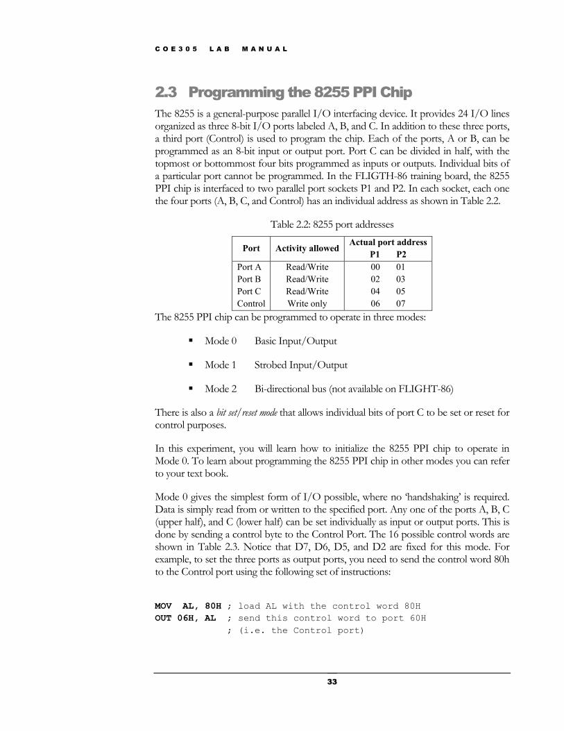
2.3 Programming the 8255 PPI Chip The 8255 is a general-purpose parallel I/O interfacing device. It provides 24 I/O lines organized as three 8-bit I/O ports labeled A, B, and C. In addition to these three ports, a third port (Control) is used to program the chip. Each of the ports, A or B, can be programmed as an 8-bit input or output port. Port C can be divided in half, with the topmost or bottommost four bits programmed as inputs or outputs. Individual bits of a particular port cannot be programmed. In the FLIGTH-86 training board, the 8255 PPI chip is interfaced to two parallel port sockets P1 and P2. In each socket, each one the four ports (A, B, C, and Control) has an individual address as shown in Table 2.2.
Table 2.2: 8255 port addresses
Port Activity allowed Actual port address P1 P2
Port A Port B Port C Control
Read/Write Read/Write Read/Write Write only
00 01 02 03 04 05 06 07
The 8255 PPI chip can be programmed to operate in three modes:
Mode 0 Basic Input/Output
Mode 1 Strobed Input/Output
Mode 2 Bi-directional bus (not available on FLIGHT-86)
There is also a bit set/reset mode that allows individual bits of port C to be set or reset for control purposes.
In this experiment, you will learn how to initialize the 8255 PPI chip to operate in Mode 0. To learn about programming the 8255 PPI chip in other modes you can refer to your text book.
Mode 0 gives the simplest form of I/O possible, where no ‘handshaking’ is required. Data is simply read from or written to the specified port. Any one of the ports A, B, C (upper half), and C (lower half) can be set individually as input or output ports. This is done by sending a control byte to the Control Port. The 16 possible control words are shown in Table 2.3. Notice that D7, D6, D5, and D2 are fixed for this mode. For example, to set the three ports as output ports, you need to send the control word 80h to the Control port using the following set of instructions:
MOV AL, 80H ; load AL with the control word 80H OUT 06H, AL ; send this control word to port 60H ; (i.e. the Control port)

C O E 3 0 5 L A B M A N U A L
34
Table 2.3: Control words for Mode 0
Ports Control Word A C (higher) B C (lower) D7 D6 D5 D4 D3 D2 D1 D0
OUT OUT OUT OUT OUT OUT OUT OUT IN IN IN IN IN IN IN IN
OUT OUT OUT OUT
IN IN IN IN
OUT OUT OUT OUT
IN IN IN IN
OUT OUT IN IN
OUT OUT IN IN
OUT OUT IN IN
OUT OUT IN IN
OUT IN
OUT IN
OUT IN
OUT IN
OUT IN
OUT IN
OUT IN
OUT IN
1 0 0 0 0 0 0 0 1 0 0 0 0 0 0 1 1 0 0 0 0 0 1 0 1 0 0 0 0 0 1 1 1 0 0 0 1 0 0 0 1 0 0 0 1 0 0 1 1 0 0 0 1 0 1 0 1 0 0 0 1 0 1 1 1 0 0 1 0 0 0 0 1 0 0 1 0 0 0 1 1 0 0 1 0 0 1 0 1 0 0 1 0 0 1 1 1 0 0 1 1 0 0 0 1 0 0 1 1 0 0 1 1 0 0 1 1 0 1 0 1 0 0 1 1 0 1 1
2.4 Conducting Simple Experiments Using the Application Board
In this section, you will learn how to write simple programs to read the states of the switches and turn on/off the LEDs on the Application Board connected to the FLIGHT-86 training board. These programs will be assembled on the PC, and then downloaded to the training board. In this way, you can keep your programs on the PC, and easily modify them or link them with other programs.
Example 2.1: Write a program to read the state of a switch (on/off) and display it on the corresponding LED. 1 2 3 4 5 6 7 8 9 10 11
COMSEG SEGMENT BYTE PUBLIC 'CODE' ASSUME CS:COMSEG, DS:COMSEG, ES:COMSEG, SS:COMSEG ORG 0100h start: MOV AL, 99h; Port A IN, Port B OUT, Port C OUT OUT 06h, AL; output control word to the Control Port L1: IN AL, 00h; read the states of the switches OUT 02h, AL; display the output on the LEDs JMP L1 COMSEG ENDS END start

C O E 3 0 5 L A B M A N U A L
35
Lines 4 and 5 in the above code initialize the 8255 PPI chip in Mode 0, such that ports A and C are set as input ports while port B is set as an output port. Then, the program enters a continuous loop that reads the states of the switches into AL and displays them on the LEDs. Reading the states of the switches (line 7) is done through port A (00h), while displaying the output on the LEDs (line 8) is done through port B (02h).
Example 2.2: Write a program to generate modulo 16 counter and display the output on the LEDs. 1 2 3 4 5 6 7 8 9 10 11 12 13 14 15 16 17 18
COMSEG SEGMENT BYTE PUBLIC 'CODE' ASSUME CS:COMSEG, DS:COMSEG, ES:COMSEG, SS:COMSEG ORG 0100h start: MOV BL, 16 MOV AL, 99h ; Port A IN, Port B OUT, Port C OUT OUT 06h, AL ; output control word to the Control Port MOV AX, 0 ; initialize the counter to 0 L1: OUT 02h, AL ; display the counter on the LEDs MOV CX, 0FFFh ; delay loop L2: LOOP L2 INC AL ; increment the counter DIV BL ; AH = AL mod 16 MOV AL, AH MOV AH, 0 JMP L1 COMSEG ENDS END start
The previous code starts as usual by initializing the 8255 PPI chip (lines 6 and 7). The counter is initialized in line 8. Line 9 displays the counter on the LEDs through port B (02h). Then, the program enters a delay loop (lines 10 to 12) before incrementing the counter in line 13. Since a module 16 counting is required, the counter (i.e. AX) is divided by 16 and the remainder is loaded back into AX (lines 14 to 16). Notice that instruction in line 14 divides AX by 16, leaving the quotient in AL and the remainder in AH.

C O E 3 0 5 L A B M A N U A L
36
Exercises 2.1. Write a program to generate the following based on the state of a particular
switch
Switch 1 : ON Generate a mod 8 counter and display it on LEDs
OFF Switch off all LEDs
Switch 2 : ON Generate a mod 256 counter and display it on LEDs
OFF Switch off all LEDs
Switch 3 : ON Light LEDs one after another one at a time in a sequence from left to right (from first LED to Last LED). When one LED is on, all other LEDs must be switched off. ( i.e., shifting bit ‘1’ from left to right). Repeat this cycle until the switch 3 is turned OFF
Switch 4 : ON Repeat the above from last LED to the first
2.2. Write a program to add 2 four-bit numbers and display the result on the LEDs. The two numbers are entered through the 8-DIP switch provided on the Application Board (i.e. each 4 switches represent one number).
Related Documents