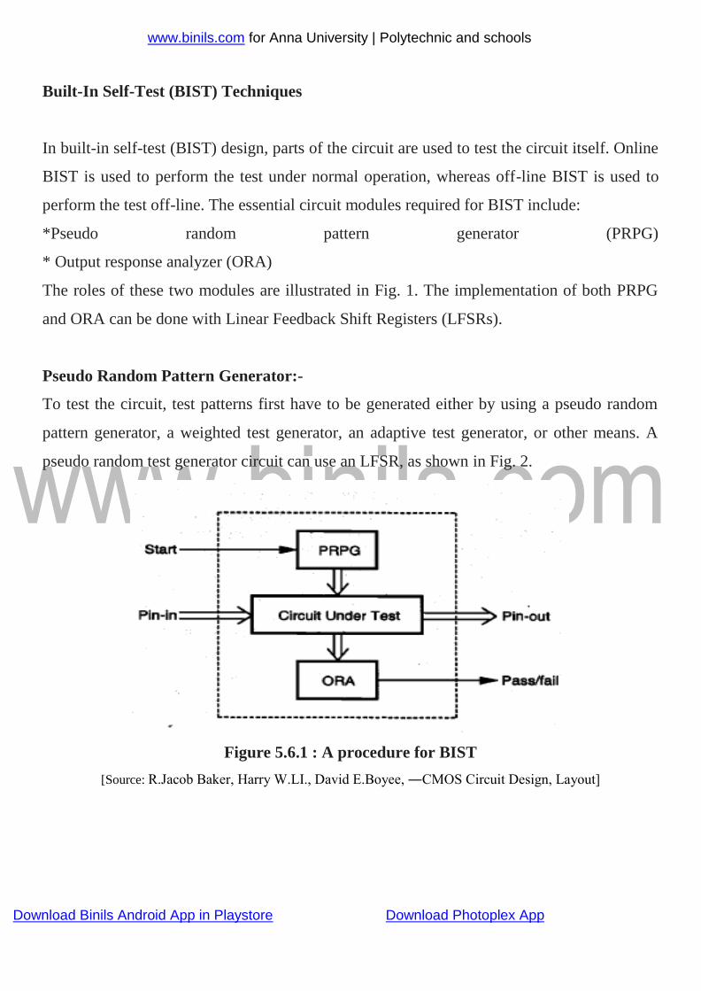
www.binils.com for Anna University | Polytechnic and schools Download Binils Android App in Playstore Download Photoplex App Built-In Self-Test (BIST) Techniques In built-in self-test (BIST) design, parts of the circuit are used to test the circuit itself. Online BIST is used to perform the test under normal operation, whereas off-line BIST is used to perform the test off-line. The essential circuit modules required for BIST include: *Pseudo random pattern generator (PRPG) * Output response analyzer (ORA) The roles of these two modules are illustrated in Fig. 1. The implementation of both PRPG and ORA can be done with Linear Feedback Shift Registers (LFSRs). Pseudo Random Pattern Generator:- To test the circuit, test patterns first have to be generated either by using a pseudo random pattern generator, a weighted test generator, an adaptive test generator, or other means. A pseudo random test generator circuit can use an LFSR, as shown in Fig. 2. Figure 5.6.1 : A procedure for BIST [Source: R.Jacob Baker, Harry W.LI., David E.Boyee, ―CMOS Circuit Design, Layout]

Welcome message from author
This document is posted to help you gain knowledge. Please leave a comment to let me know what you think about it! Share it to your friends and learn new things together.
Transcript
www.binils.com for Anna University | Polytechnic and schools
Download Binils Android App in Playstore Download Photoplex App
Built-In Self-Test (BIST) Techniques
In built-in self-test (BIST) design, parts of the circuit are used to test the circuit itself. Online
BIST is used to perform the test under normal operation, whereas off-line BIST is used to
perform the test off-line. The essential circuit modules required for BIST include:
*Pseudo random pattern generator (PRPG)
* Output response analyzer (ORA)
The roles of these two modules are illustrated in Fig. 1. The implementation of both PRPG
and ORA can be done with Linear Feedback Shift Registers (LFSRs).
Pseudo Random Pattern Generator:-
To test the circuit, test patterns first have to be generated either by using a pseudo random
pattern generator, a weighted test generator, an adaptive test generator, or other means. A
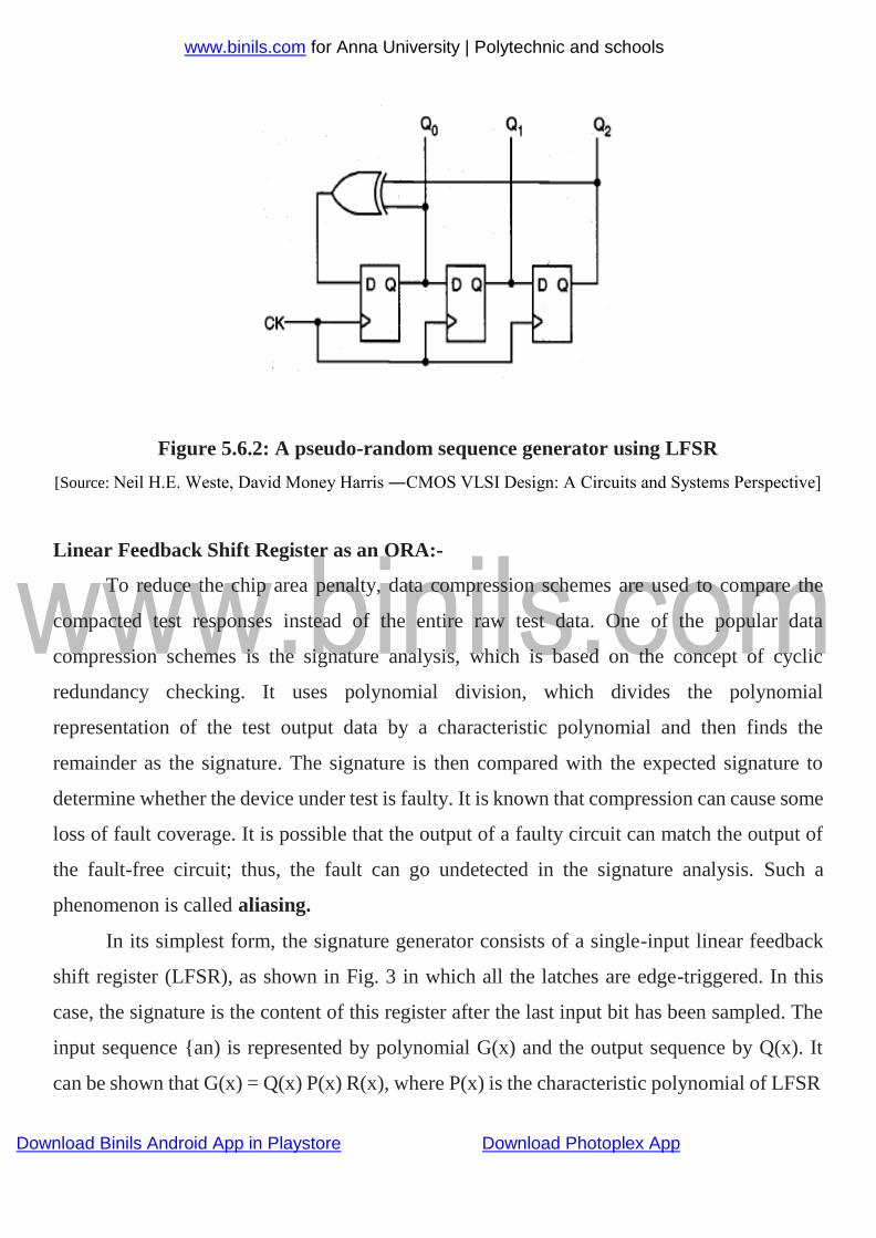
pseudo random test generator circuit can use an LFSR, as shown in Fig. 2.
Figure 5.6.1 : A procedure for BIST
[Source: R.Jacob Baker, Harry W.LI., David E.Boyee, ―CMOS Circuit Design, Layout]
www.binils.com for Anna University | Polytechnic and schools
Download Binils Android App in Playstore Download Photoplex App
Figure 5.6.2: A pseudo-random sequence generator using LFSR
[Source: Neil H.E. Weste, David Money Harris ―CMOS VLSI Design: A Circuits and Systems Perspective]
Linear Feedback Shift Register as an ORA:-
To reduce the chip area penalty, data compression schemes are used to compare the
compacted test responses instead of the entire raw test data. One of the popular data
compression schemes is the signature analysis, which is based on the concept of cyclic
redundancy checking. It uses polynomial division, which divides the polynomial
representation of the test output data by a characteristic polynomial and then finds the
remainder as the signature. The signature is then compared with the expected signature to
determine whether the device under test is faulty. It is known that compression can cause some
loss of fault coverage. It is possible that the output of a faulty circuit can match the output of
the fault-free circuit; thus, the fault can go undetected in the signature analysis. Such a
phenomenon is called aliasing.
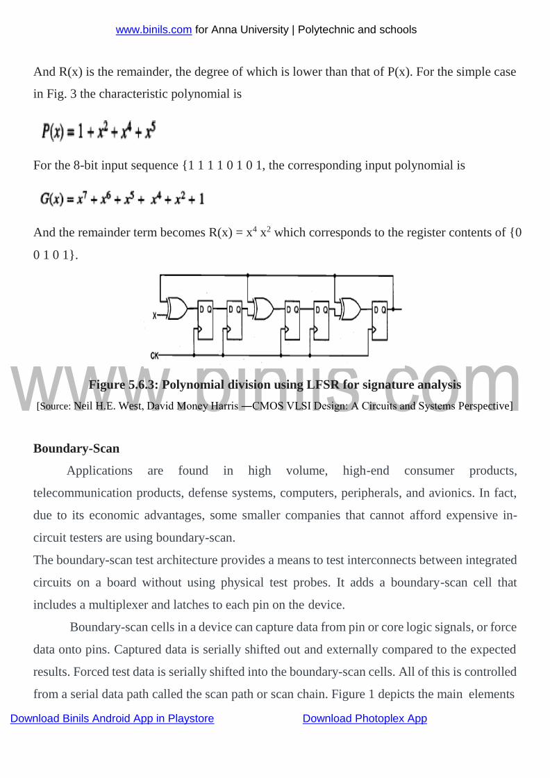
In its simplest form, the signature generator consists of a single-input linear feedback
shift register (LFSR), as shown in Fig. 3 in which all the latches are edge-triggered. In this
case, the signature is the content of this register after the last input bit has been sampled. The
input sequence {an) is represented by polynomial G(x) and the output sequence by Q(x). It
can be shown that G(x) = Q(x) P(x) R(x), where P(x) is the characteristic polynomial of LFSR
www.binils.com for Anna University | Polytechnic and schools
Download Binils Android App in Playstore Download Photoplex App
And R(x) is the remainder, the degree of which is lower than that of P(x). For the simple case
in Fig. 3 the characteristic polynomial is
For the 8-bit input sequence {1 1 1 1 0 1 0 1, the corresponding input polynomial is
And the remainder term becomes R(x) = x4 x2 which corresponds to the register contents of {0
0 1 0 1}.
Figure 5.6.3: Polynomial division using LFSR for signature analysis
[Source: Neil H.E. West, David Money Harris ―CMOS VLSI Design: A Circuits and Systems Perspective]
Boundary-Scan
Applications are found in high volume, high-end consumer products,
telecommunication products, defense systems, computers, peripherals, and avionics. In fact,
due to its economic advantages, some smaller companies that cannot afford expensive in-
circuit testers are using boundary-scan.
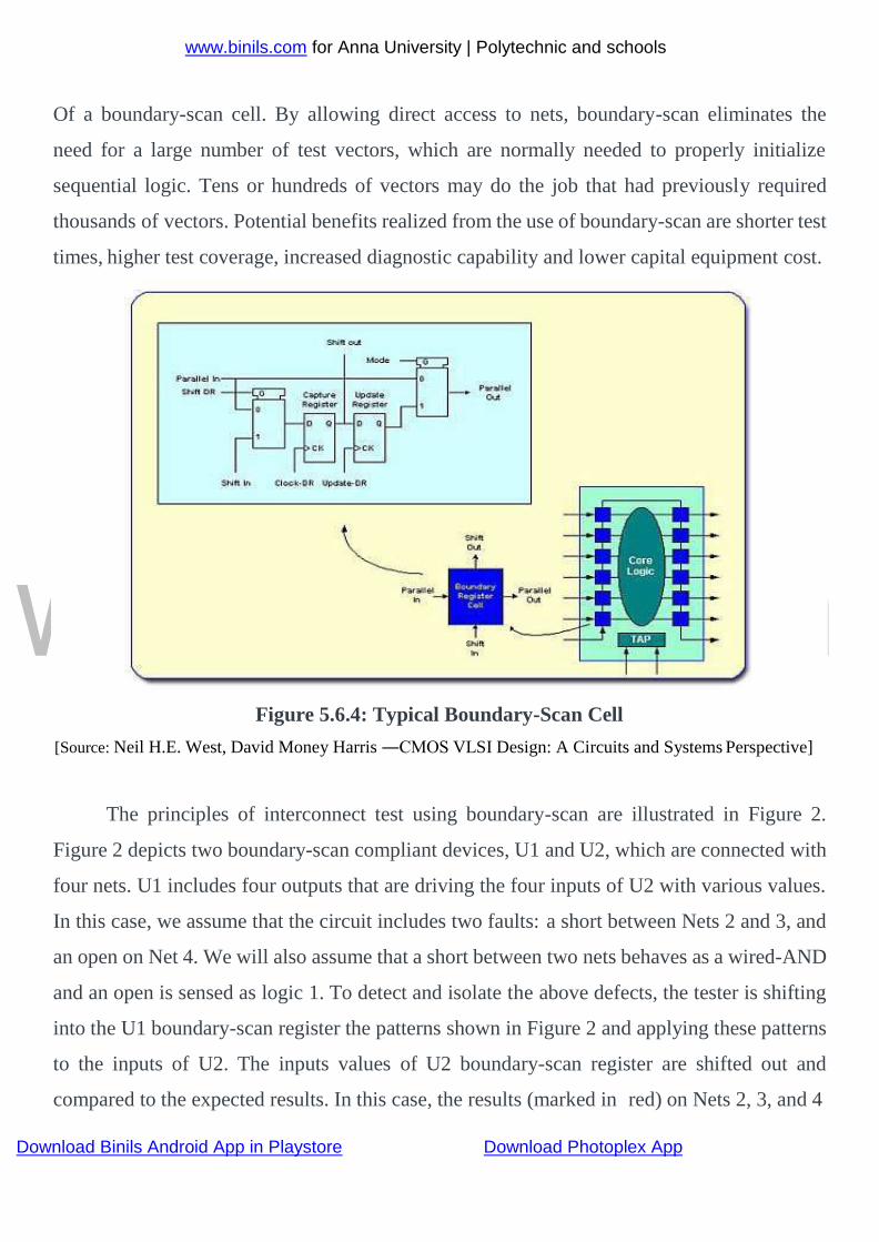
The boundary-scan test architecture provides a means to test interconnects between integrated
circuits on a board without using physical test probes. It adds a boundary-scan cell that
includes a multiplexer and latches to each pin on the device.
Boundary-scan cells in a device can capture data from pin or core logic signals, or force
data onto pins. Captured data is serially shifted out and externally compared to the expected
results. Forced test data is serially shifted into the boundary-scan cells. All of this is controlled
from a serial data path called the scan path or scan chain. Figure 1 depicts the main elements
www.binils.com for Anna University | Polytechnic and schools
Download Binils Android App in Playstore Download Photoplex App
Of a boundary-scan cell. By allowing direct access to nets, boundary-scan eliminates the
need for a large number of test vectors, which are normally needed to properly initialize
sequential logic. Tens or hundreds of vectors may do the job that had previously required
thousands of vectors. Potential benefits realized from the use of boundary-scan are shorter test
times, higher test coverage, increased diagnostic capability and lower capital equipment cost.
[Source: Neil H.E. West, David Money Harris ―CMOS VLSI Design: A Circuits and Systems Perspective]
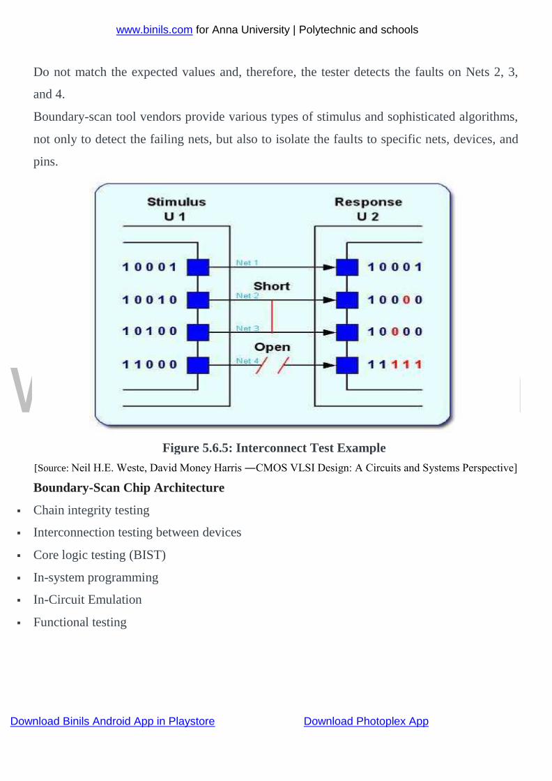
The principles of interconnect test using boundary-scan are illustrated in Figure 2.
Figure 2 depicts two boundary-scan compliant devices, U1 and U2, which are connected with
four nets. U1 includes four outputs that are driving the four inputs of U2 with various values.
In this case, we assume that the circuit includes two faults: a short between Nets 2 and 3, and
an open on Net 4. We will also assume that a short between two nets behaves as a wired-AND
and an open is sensed as logic 1. To detect and isolate the above defects, the tester is shifting
into the U1 boundary-scan register the patterns shown in Figure 2 and applying these patterns
to the inputs of U2. The inputs values of U2 boundary-scan register are shifted out and
compared to the expected results. In this case, the results (marked in red) on Nets 2, 3, and 4
Figure 5.6.4: Typical Boundary-Scan Cell
www.binils.com for Anna University | Polytechnic and schools
Download Binils Android App in Playstore Download Photoplex App
Do not match the expected values and, therefore, the tester detects the faults on Nets 2, 3,
and 4.
Boundary-scan tool vendors provide various types of stimulus and sophisticated algorithms,
not only to detect the failing nets, but also to isolate the faults to specific nets, devices, and
pins.
[Source: Neil H.E. Weste, David Money Harris ―CMOS VLSI Design: A Circuits and Systems Perspective]
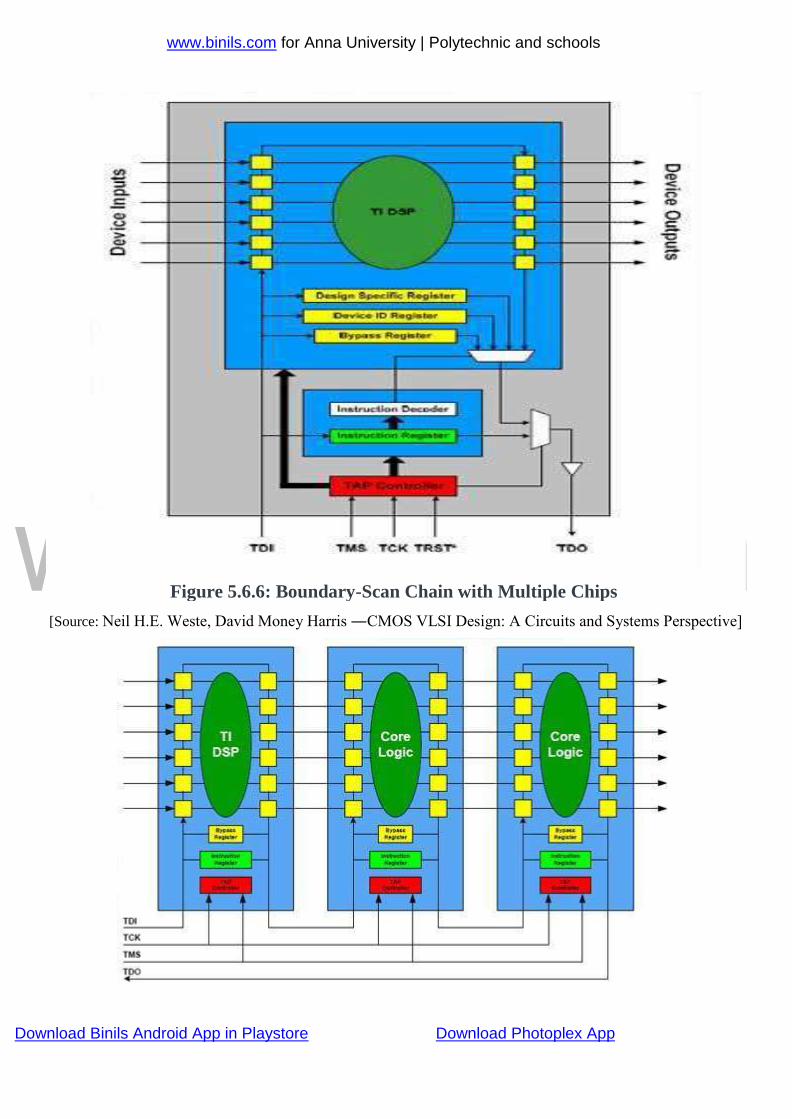
Boundary-Scan Chip Architecture
Chain integrity testing
Interconnection testing between devices
Core logic testing (BIST)
In-system programming
In-Circuit Emulation
Functional testing
Figure 5.6.5: Interconnect Test Example
www.binils.com for Anna University | Polytechnic and schools
Download Binils Android App in Playstore Download Photoplex App
[Source: Neil H.E. Weste, David Money Harris ―CMOS VLSI Design: A Circuits and Systems Perspective]
Figure 5.6.6: Boundary-Scan Chain with Multiple Chips
www.binils.com for Anna University | Polytechnic and schools
Download Binils Android App in Playstore Download Photoplex App
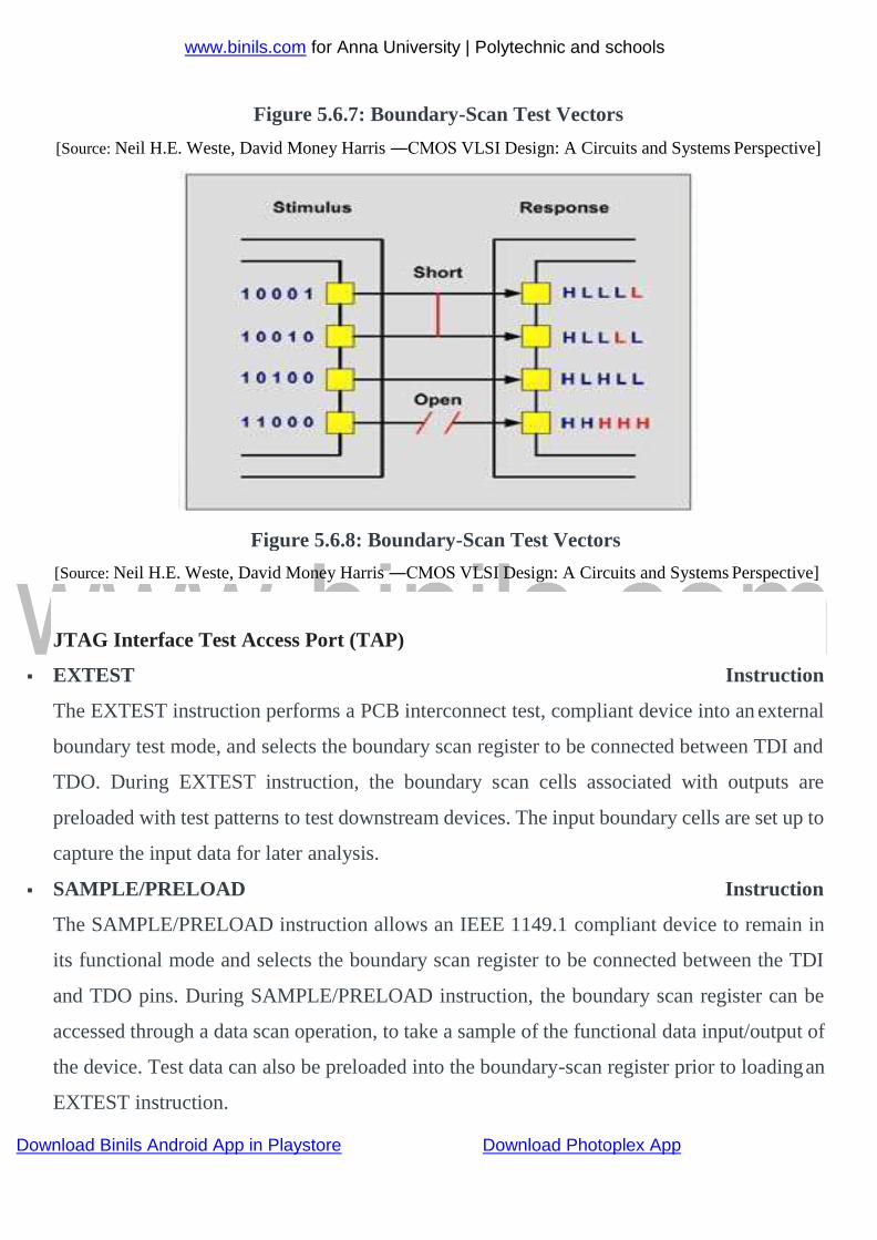
Figure 5.6.8: Boundary-Scan Test Vectors
Figure 5.6.7: Boundary-Scan Test Vectors
[Source: Neil H.E. Weste, David Money Harris ―CMOS VLSI Design: A Circuits and Systems Perspective]
[Source: Neil H.E. Weste, David Money Harris ―CMOS VLSI Design: A Circuits and Systems Perspective]
JTAG Interface Test Access Port (TAP)
EXTEST Instruction
The EXTEST instruction performs a PCB interconnect test, compliant device into an external
boundary test mode, and selects the boundary scan register to be connected between TDI and
TDO. During EXTEST instruction, the boundary scan cells associated with outputs are
preloaded with test patterns to test downstream devices. The input boundary cells are set up to
capture the input data for later analysis.
SAMPLE/PRELOAD Instruction
The SAMPLE/PRELOAD instruction allows an IEEE 1149.1 compliant device to remain in
its functional mode and selects the boundary scan register to be connected between the TDI
and TDO pins. During SAMPLE/PRELOAD instruction, the boundary scan register can be
accessed through a data scan operation, to take a sample of the functional data input/output of
the device. Test data can also be preloaded into the boundary-scan register prior to loading an
EXTEST instruction.
www.binils.com for Anna University | Polytechnic and schools
Download Binils Android App in Playstore Download Photoplex App
BYPASS Instruction
Using the BYPASS instruction, a device’s boundary scan chain can be skipped, allowing the
data to pass through the bypass register. This allows efficient testing of a selected device
without incurring the overhead of traversing through other devices. The BYPASS instruction
allows an IEEE 1149.1 compliant device to remain in a functional mode and selects the bypass
register to be connected between the TDI and TDO pins. Serial data is allowed to be transferred
through a device from the TDI pin to the TDO pin without affecting the operation of the device.
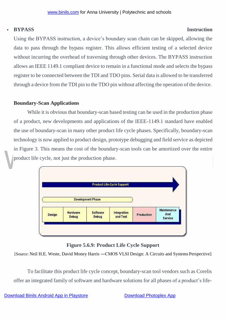
Boundary-Scan Applications
While it is obvious that boundary-scan based testing can be used in the production phase
of a product, new developments and applications of the IEEE-1149.1 standard have enabled
the use of boundary-scan in many other product life cycle phases. Specifically, boundary-scan
technology is now applied to product design, prototype debugging and field service as depicted
in Figure 3. This means the cost of the boundary-scan tools can be amortized over the entire
product life cycle, not just the production phase.
Figure 5.6.9: Product Life Cycle Support
[Source: Neil H.E. Weste, David Money Harris ―CMOS VLSI Design: A Circuits and Systems Perspective]
To facilitate this product life cycle concept, boundary-scan tool vendors such as Corelis
offer an integrated family of software and hardware solutions for all phases of a product’s life-
www.binils.com for Anna University | Polytechnic and schools
Download Binils Android App in Playstore Download Photoplex App
Cycle. All of these products are compatible with each other, thus protecting the user’s
investment.
Applying Boundary-Scan for Product Development
The ongoing marketing drive for reduced product size, such as portable phones and
digital cameras, higher functional integration, faster clock rates, and shorter product life-cycle
with dramatically faster time-to- market has created new technology trends. These trends
include increased device complexity, fine pitch components, such as surface-mount
technology (SMT), systems-in-package (SIPs), multi-chip modules (MCMs), ball-grid arrays
(BGAs), increased IC pin-count, and smaller PCB traces. These technology advances, in turn,
create problems in PCB development:
Many boards include components that are assembled on both sides of the board. Most of the
through-holes and traces are buried and inaccessible.
Loss of physical access to fine pitch components, such as SMTs and BGAs, makes it difficult
to probe the pins and distinguish between manufacturing and design problems.
Often a prototype board is hurriedly built by a small assembly shop with lower quality control
as compared to a production house. A prototype generally will include more assembly defects
than a production unit.
When the prototype arrives, a test fixture for the ICT is not available and, therefore,
manufacturing defects cannot be easily detected and isolated.
Small-size products do not have test points, making it difficult or impossible to probe
suspected nodes.
Many Complex Programmable Logic Devices (CPLDs) and flash memory devices (in BGA
packages) are not socketed and are soldered directly to the board.
Every time a new processor or a different flash device is selected, the engineer has to learn
from scratch how to program the flash memory.
When a design includes CPLDs from different vendors, the engineer must use different in-
circuit programmers to program the CPLDs.
Boundary-scan technology is the only cost-effective solution that can deal with the above
problems. In recent years, the number of devices that include boundary-scan has grown
www.binils.com for Anna University | Polytechnic and schools
Download Binils Android App in Playstore Download Photoplex App
Dramatically. Almost every new microprocessor that is being introduced includes boundary-
scan circuitry for testing and in-circuit emulation. Most of the CPLD and field programmable
array (FPGA) manufacturers, such as Altera, Lattice and Xilinx, to mention a few, have
incorporated boundary-scan logic into their components, including additional circuitry that
uses the boundary-scan four-wire interface to program their devices in-system.
As the acceptance of boundary-scan as the main technology for interconnect testing and in-
system programming (ISP) has increased, the various boundary-scan test and ISP tools have
matured as well. The increased number of boundary-scan components and mature boundary-
scan tools, as well as other factors that will be described later, provide engineers with the
following benefits:
Easy to implement Design-For- Testability (DFT) rules. A list of basic DFT rules is provided
later in this article.
Design analysis prior to PCB layout to improve testability.
Packaging problems are found prior to PCB layout.
Little need for test points.
No need for test fixtures.
More control over the test process.
Quick diagnosis (with high resolution) of interconnection problems without writing any
functional test code.
Program code in flash devices.
Design configuration data placement into CPLDs.
JTAG emulation and source-level debugging.
What Boundary-Scan Tools are needed?
In the previous section, we listed many of the benefits that a designer enjoys when
incorporating boundary-scan in his product development. In this section we describe the tools
and design data needed to develop boundary-scan test procedures and patterns for ISP,
followed by a description of how to test and program a board. We use a typical board as an
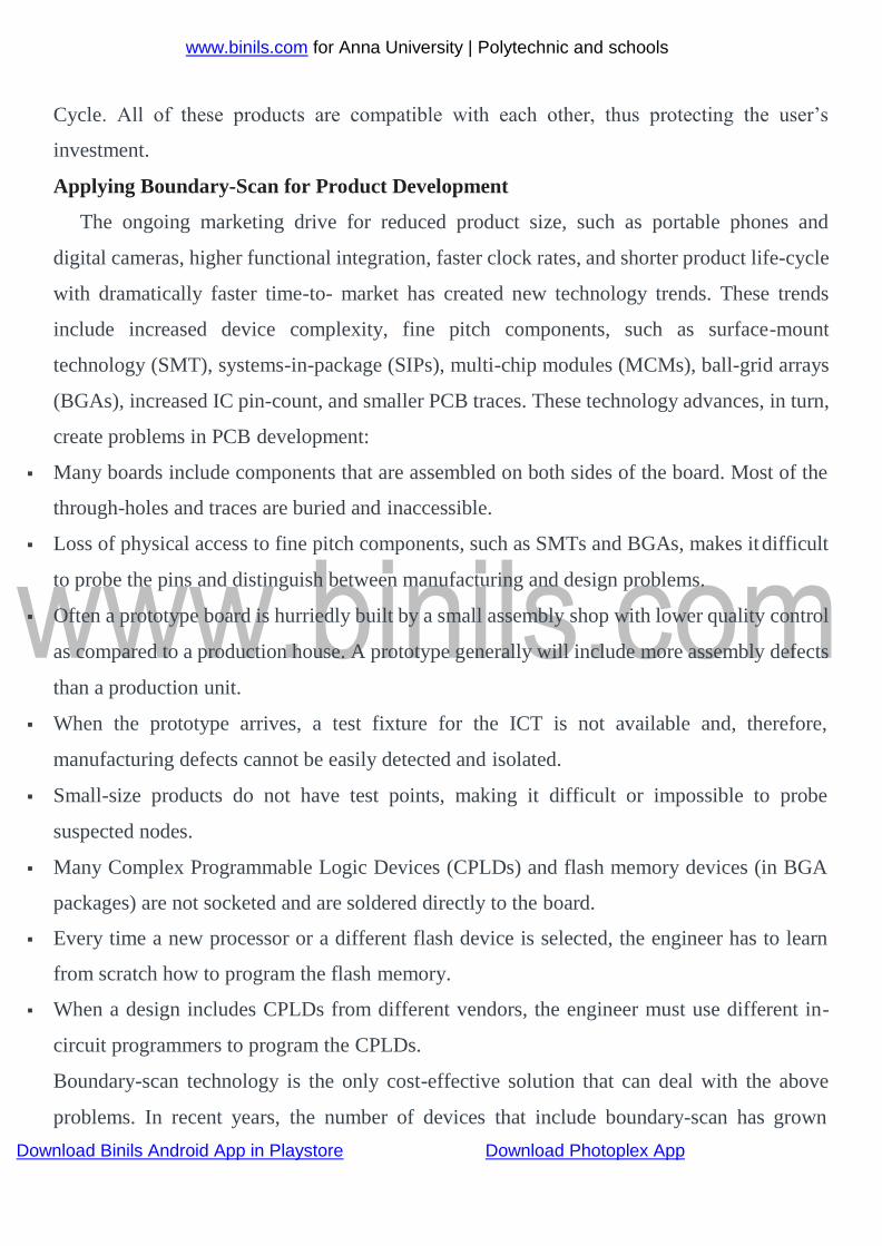
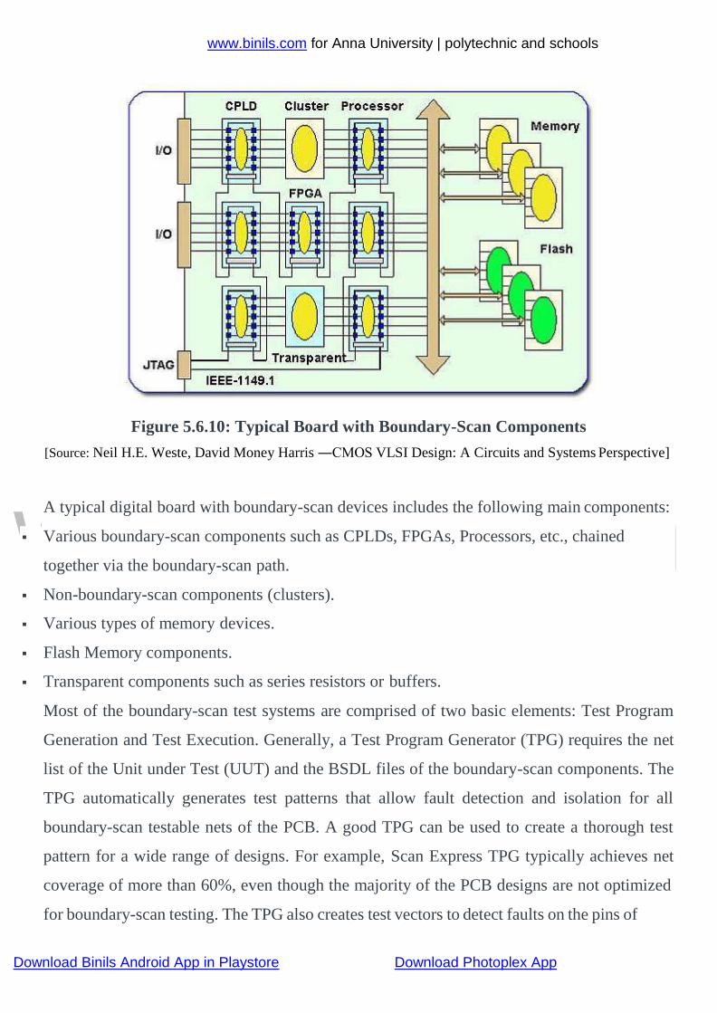
illustration for the various boundary-scan test functions needed. A block diagram of such a
board is depicted in Figure 4.
www.binils.com for Anna University | polytechnic and schools
[Source: Neil H.E. Weste, David Money Harris ―CMOS VLSI Design: A Circuits and Systems Perspective]
A typical digital board with boundary-scan devices includes the following main components:
Various boundary-scan components such as CPLDs, FPGAs, Processors, etc., chained
together via the boundary-scan path.
Non-boundary-scan components (clusters).
Various types of memory devices.
Flash Memory components.
Transparent components such as series resistors or buffers.
Most of the boundary-scan test systems are comprised of two basic elements: Test Program
Generation and Test Execution. Generally, a Test Program Generator (TPG) requires the net
list of the Unit under Test (UUT) and the BSDL files of the boundary-scan components. The
TPG automatically generates test patterns that allow fault detection and isolation for all
boundary-scan testable nets of the PCB. A good TPG can be used to create a thorough test
pattern for a wide range of designs. For example, Scan Express TPG typically achieves net
coverage of more than 60%, even though the majority of the PCB designs are not optimized
for boundary-scan testing. The TPG also creates test vectors to detect faults on the pins of
Download Binils Android App in Playstore Download Photoplex App
Figure 5.6.10: Typical Board with Boundary-Scan Components
www.binils.com for Anna University | polytechnic and schools
Download Binils Android App in Playstore Download Photoplex App
Scan able components, such as clusters and memories that are surrounded by scan able
devices.
Some TPGs also generate a test coverage report that allows the user to focus on the non-
testable nets and determine what additional means are needed to increase the test coverage.
Test programs are generated in seconds. For example, when Corelli’s Scan Express TPG™
was used, it took a 3.0 GHz Pentium 4 PC 23 seconds to generate an interconnect test for a
UUT with 5,638 nets (with 19,910 pins). This generation time includes net list and all other
input files processing as well as test pattern file generation.
Test execution tools from various vendors provide means for executing boundary-scan tests
and performing in-system programming in a pre-planned specific order, called a test plan. Test
vectors files, which have been generated using the TPG, are automatically applied to the UUT
and the results are compared to the expected values. In case of a detected fault, the system
diagnoses the fault and lists the failures as depicted in Figure 5. Figure 5 shows the main
window of the Corelli’s test execution tool, Scan Express Runner™. Scan Express Runner
gives the user an overview of all test steps and the results of executed tests. These results are
displayed both for individual tests as well as for the total test runs executed. Scan Express
Runner provides the ability to add or delete various test steps from a test plan, or re-arrange
the order of the test steps in a plan. Tests can also be enabled or disabled and the test execution
can be stopped upon the failure of any particular test.
Different test plans may be constructed for different UUTs. Tests within a test plan may be re-
ordered, enabled or disabled, and unlimited different tests can be combined into a test plan.
Scan Express Runner can be used to develop a test sequence or test plan from various
independent sub-tests. These sub-tests can then be executed sequentially as many times as
specified or continuously if desired. A sub-test can also program CPLDs and flash memories.
For ISP, other formats, such as SVF, JAM, and STAPL, are also supported.
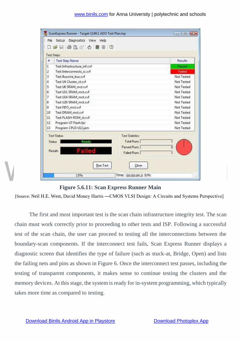
To test the board depicted in Figure 5.6.10, the user must execute a test plan that consists of
various test steps as shown in Figure 5.6.11.
www.binils.com for Anna University | polytechnic and schools
Download Binils Android App in Playstore Download Photoplex App
[Source: Neil H.E. West, David Money Harris ―CMOS VLSI Design: A Circuits and Systems Perspective]
The first and most important test is the scan chain infrastructure integrity test. The scan
chain must work correctly prior to proceeding to other tests and ISP. Following a successful
test of the scan chain, the user can proceed to testing all the interconnections between the
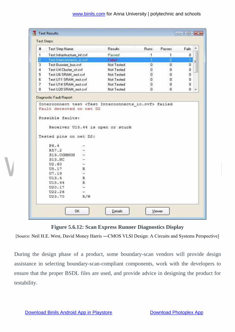
boundary-scan components. If the interconnect test fails, Scan Express Runner displays a
diagnostic screen that identifies the type of failure (such as stuck-at, Bridge, Open) and lists
the failing nets and pins as shown in Figure 6. Once the interconnect test passes, including the
testing of transparent components, it makes sense to continue testing the clusters and the
memory devices. At this stage, the system is ready for in-system programming, which typically
takes more time as compared to testing.
Figure 5.6.11: Scan Express Runner Main Window
www.binils.com for Anna University | polytechnic and schools
Download Binils Android App in Playstore Download Photoplex App
Figure 5.6.12: Scan Express Runner Diagnostics Display
[Source: Neil H.E. West, David Money Harris ―CMOS VLSI Design: A Circuits and Systems Perspective]
During the design phase of a product, some boundary-scan vendors will provide design
assistance in selecting boundary-scan-compliant components, work with the developers to
ensure that the proper BSDL files are used, and provide advice in designing the product for
testability.
www.binils.com for Anna University | polytechnic and schools
Download Binils Android App in Playstore Download Photoplex App
Applying Boundary-Scan for Production Test
Production testing, utilizing traditional In-Circuit Testers that do not have boundary-scan
features installed, experience similar problems that the product developer had and more:
Loss of physical access to fine pitch components, such as SMTs and BGAs, reduces bed-of-
nails ICT fault isolation.
Development of test fixtures for ICTs becomes longer and more expensive.
Development of test procedures for ICTs becomes longer and more expensive due to more
complex ICs.
Designers are forced to bring out a large number of test points, which is in direct conflict with
the goal to miniaturize the design.
In-system programming is inherently slow, inefficient, and expensive if done with an ICT.
Assembling boards with BGAs is difficult and subject to numerous defects, such as solder
smearing.
<JTAG Embedded Functional Test/h3>
Recently, a test methodology has been developed which combines the ease-of-use and low
cost of boundary-scan with the coverage and security of traditional functional testing. This
new technique, called JTAG Emulation Test (JET), lets engineers automatically develop PCB
functional test that can be run at full speed., If the PCB has an on-board processor with a JTAG
port (common, even if the processor doesn’t support boundary-scan), JET and boundary-scan
tests can be executed as part of the same test plan to provide extended fault coverage to further
complement or replace ICT testing.
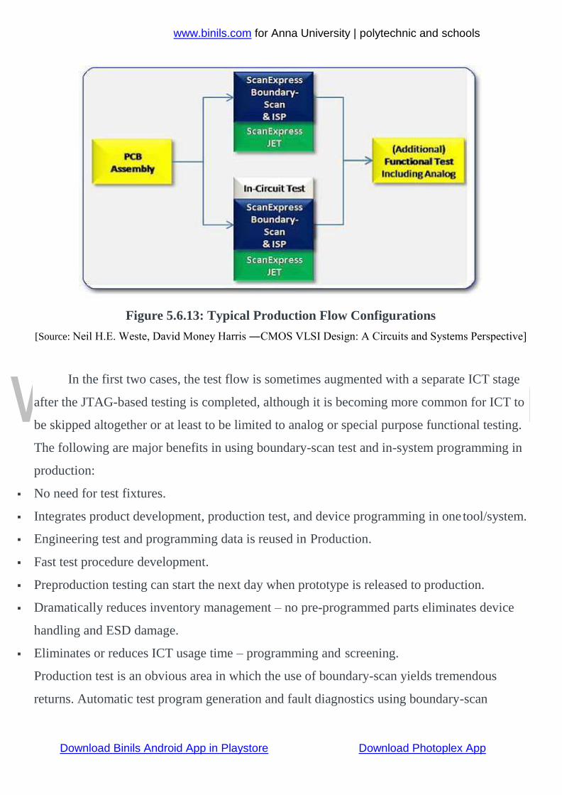
The diagram shows two typical ways that boundary-scan is deployed:
As a stand-alone application at a separate test station or test bench to test all the inter
connects and perform ISP of on-board flash and other memories. JTAG embedded functional
test (JET) may be integrated with boundary-scan.
Integrated into the ICT system, where the JTAG control hardware is embedded in the ICT
system and the boundary-scan (and possibly JET) software is a module called from the ICT
software system.
www.binils.com for Anna University | polytechnic and schools
Download Binils Android App in Playstore Download Photoplex App
[Source: Neil H.E. Weste, David Money Harris ―CMOS VLSI Design: A Circuits and Systems Perspective]
In the first two cases, the test flow is sometimes augmented with a separate ICT stage
after the JTAG-based testing is completed, although it is becoming more common for ICT to
be skipped altogether or at least to be limited to analog or special purpose functional testing.
The following are major benefits in using boundary-scan test and in-system programming in
production:
No need for test fixtures.
Integrates product development, production test, and device programming in one tool/system.
Engineering test and programming data is reused in Production.
Fast test procedure development.
Preproduction testing can start the next day when prototype is released to production.
Dramatically reduces inventory management – no pre-programmed parts eliminates device
handling and ESD damage.
Eliminates or reduces ICT usage time – programming and screening.
Production test is an obvious area in which the use of boundary-scan yields tremendous
returns. Automatic test program generation and fault diagnostics using boundary-scan
Figure 5.6.13: Typical Production Flow Configurations
www.binils.com for Anna University | polytechnic and schools
Download Binils Android App in Playstore Download Photoplex App
Software products and the lack of expensive featuring requirements can make the entire test
process very economical. For products that contain edge connectors and digital interfaces that
are not visible from the boundary-scan chain, boundary-scan vendors offer a family of
boundary-scan controllable I/Oz that provide a low cost alternative to expensive digital pin
electronics.
Field Service and Installation
The role of boundary-scan does not end when a product ships. Periodic software and
hardware updates can be performed remotely using the boundary-scan chain as a non-intrusive
access mechanism. This allows flash updates and reprogramming of programmable logic, for
example. Service centers that normally would not want to invest in special equipment to
support a product now have an option of using a standard PC or laptop for boundary-scan
testing. A simple PC-based boundary-scan controller can be used for all of the above tasks and
also double as a fault diagnostic system, using the same test vectors that were developed during
the design and production phase. This concept can be taken one step further by allowing an
embedded processor access to the boundary-scan chain. This allows diagnostics and fault
isolation to be performed by the embedded processor. The same diagnostic routines can be run
as part of a power-on self-test procedure.
Boundary-Scan Design-for-Test Basic Considerations
As mentioned earlier in this article, the design for boundary-scan test guidelines are
simple to understand and follow compared to other traditional test requirements. It is important
to remember that boundary-scan testing is most successful when the design and test
engineering teams work together to ensure that testability is “designed in” from the start. The
boundary-scan chain is the most critical part of boundary-scan implementations. When that is
properly implemented, improved testability inevitably follows.
Below is a list of basic guidelines to observe when designing a boundary-scan-testable board:
If there are programmable components in a chain, such as FPGAs, CPLDs, etc., group them
together in the chain order and place the group at either end of the chain. It is recommended
that you provide access to Test Data In (TDI) and Test Data Out (TDO) signals where the
programmable group connects to the non-programmable devices.

www.binils.com for Anna University | polytechnic and schools
Download Binils Android App in Playstore Download Photoplex App
All parts in the boundary-scan chain should have 1149.1-compliant test access ports (TAPs).
Use simple buffering for the Test Clock (TCK) and Test Mode Select (TMS) signals to
simplify test considerations for the boundary-scan TAP. The TAP signals should be buffered
to prevent clocking and drive problems.
Group similar device families and have a single level converter interface between them, TCK,
TMS, TDI, TDO, and system pins.
TCK should be properly routed to prevent skew and noise problems.
Use the standard JTAG connector on your board as depicted in Corelli’s documentation.
Ensure that BSDL files are available for each boundary-scan component that is used on your
board and that the files are validated.
Design for interconnect testing requires board-level system understanding to ensure higher test
coverage and elimination of signal level conflicts.
Determine which boundary-scan components are on the board. Change as many non-
boundary-scan components to IEEE 1149.1-compliant devices as possible in order to
maximize test coverage.
Check non-boundary-scan devices on the board and design disabling methods for the outputs
of those devices in order to prevent signal level conflicts. Connect the enable pins of the
conflicting devices to boundary-scan controllable outputs. Corelli’s tools will keep the
enable/disable outputs at a fixed disabling value during the entire test.
Ensure that your memory devices are surrounded by boundary-scan components. This will
allow you to use a test program generator, such as Scan Express TPG, to test the
interconnects of the memory devices.
Check the access to the non-boundary-scan clusters. Make sure that the clusters are surrounded
by boundary-scan components. By surrounding the non-boundary-scan clusters with
boundary-scan devices, the clusters can then be tested using a boundary-scan test tool.
If your design includes transparent components, such as series resistors or non-inverting
buffers, your test coverage can be increased by testing through these components using scan
Express TPG.

www.binils.com for Anna University | polytechnic and schools
Download Binils Android App in Playstore Download Photoplex App
Connect all I/so to boundary-scan controllable devices. This will enable the use of boundary-
scan, digital I/O module, such as the ScanIO-300LV, to test all your I/O pins, thus increasing
test coverage

www.binils.com for Anna University | Polytechnic and schools
Download Binils Android App in Playstore Download Photoplex App
Classification of ASIC.
An ASIC is classified into
1. Full custom ASIC
2. Semi-custom ASIC
Full Custom ASIC:
Full custom includes all possible logic cells and mask layers that are customized.
These are very expensive to manufacture and design.
Example is microprocessor.
In full custom ASIC an engineer design some or all logic cells, circuits, or layout specifically
for one ASIC.
Semi-Custom ASIC:
In semicustom aspic all the logic cells are predesigned and some of the mask layers are
customized. The types of semicustom ASIC are
1. Standard cell based ASIC
2. Gate array based ASIC
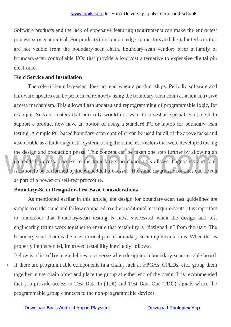
1. Standard cell based ASIC:-
A cell based ASIC or cell based IC (CBIC) uses predesigned logic cells like AND gates, OR
gates, multiplexers, Flip-flops.
The predefined logic cells are known as standard cells. The standard cell areas are called
flexible blocks
The flexible blocks used in combination with larger predesigned cells, like micro controllers
and microprocessors, these are called mega cells.
www.binils.com for Anna University | Polytechnic and schools
Download Binils Android App in Playstore Download Photoplex App
Fig 5.5.1: Cell based ASIC Advantages
[Source: R.Jacob Baker, Harry W.LI., David E.Boyee, ―CMOS Circuit Design, Layout and Simulation]
Less cost
Less time
Reduced Risk
Transistor operates at maximum speed.
Disadvantages:
Expense of designing standard cell library is high
Time needed to fabricate all layers for each new design is high.
2. Gate array based ASIC
Gate array (GA) based ASIC has predefined transistors on the silicon wafer. The predefined
pattern of transistors on a gate array is the base array. The base array is made up of a smallest
element called primitive cell.
To distinguish this type of gate array from other types of gate array ,this is often called
MASKED GATE ARRAY.(MGA)

www.binils.com for Anna University | Polytechnic and schools
Download Binils Android App in Playstore Download Photoplex App
MACROS: the logic cells in a gate array library are called macro.
The types of MGA or gate array based ASIC are
1. Channeled gate array
2. Channel less gate array
3. Structured gate array
Channeled Gate Array:
Channeled gate array has space between the rows of transistor for wiring
Features:
1. Only the inter connect is customized.
2. Interconnect uses predefined spaces between rows of base cells.
3. Manufacturing lead time is between two days and two weeks.
Fig 5.5.2: Channeled Gate Array
[Source: R.Jacob Baker, Harry W.LI., David E.Boyee, ―CMOS Circuit Design, Layout and Simulation]
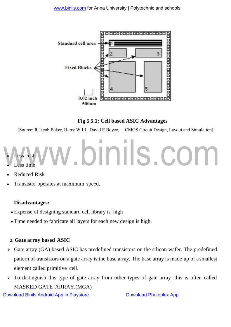
Channel less Gate Arra
www.binils.com for Anna University | Polytechnic and schools
Download Binils Android App in Playstore Download Photoplex App
The routing on a channel less gate array uses rows of unused transistors.
Features:
4. Top few mask layers are customized interconnect.
5. Manufacturing lead time is between two days and two weeks
Fig 5.5.3: Channel less Gate Array
[Source: R.Jacob Baker, Harry W.LI., David E.Boyee, ―CMOS Circuit Design, Layout and Simulation]
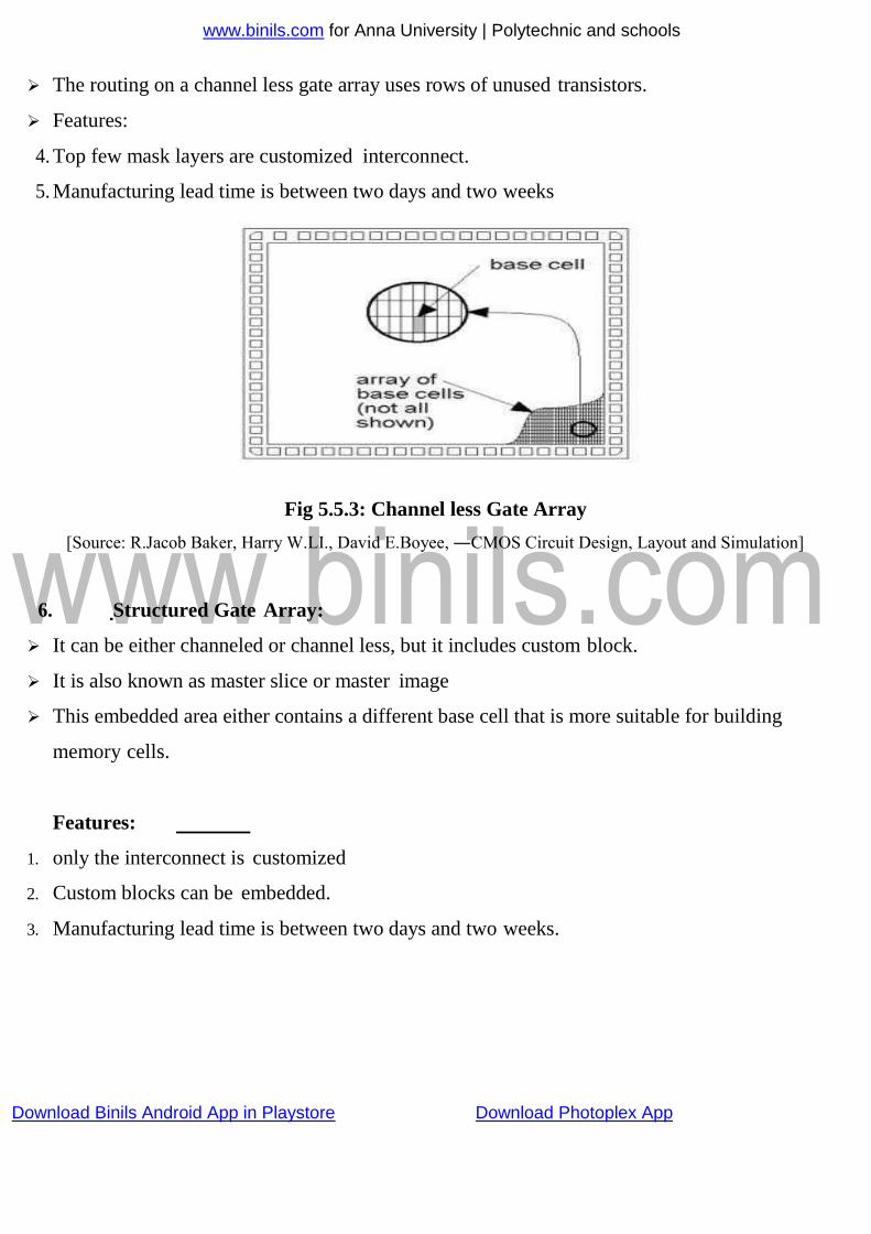
6. Structured Gate Array:
It can be either channeled or channel less, but it includes custom block.
It is also known as master slice or master image
This embedded area either contains a different base cell that is more suitable for building
memory cells.
Features:
1. only the interconnect is customized
2. Custom blocks can be embedded.
3. Manufacturing lead time is between two days and two weeks.
www.binils.com for Anna University | Polytechnic and schools
Download Binils Android App in Playstore Download Photoplex App
Fig 5.5.4: Structured Gate Array Advantages
[Source: R.Jacob Baker, Harry W.LI., David E.Boyee, ―CMOS Circuit Design, Layout and Simulation]
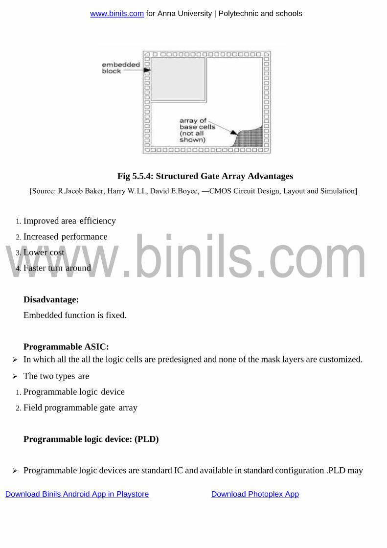
1. Improved area efficiency
2. Increased performance
3. Lower cost
4. Faster turn around
Disadvantage:
Embedded function is fixed.
Programmable ASIC:
In which all the all the logic cells are predesigned and none of the mask layers are customized.
The two types are
1. Programmable logic device
2. Field programmable gate array
Programmable logic device: (PLD)
Programmable logic devices are standard IC and available in standard configuration .PLD may

www.binils.com for Anna University | Polytechnic and schools
Download Binils Android App in Playstore Download Photoplex App
Features:
1. No customized mask layers or logic cells.
2. Fast design turnaround
3. Single large block of programmable interconnect
4. Matrix of large macro cells
Field programmable gate array: (FPGA)
Complex PLD’s are called FPGA.
FPGA are growing rapidly and replace TTL in microelectronic system
Characteristics:
1. No mask layers are customized.
2. Programming basic logic cells and interconnects.
3. Core with regular array of programmable basic logic cells that implement combinational and
sequential logic.
4. Matrix of programmable interconnect surrounds the basic logic cells.
5. Programmable I/O cells surround the core.
6. Design turnaround is few hours.
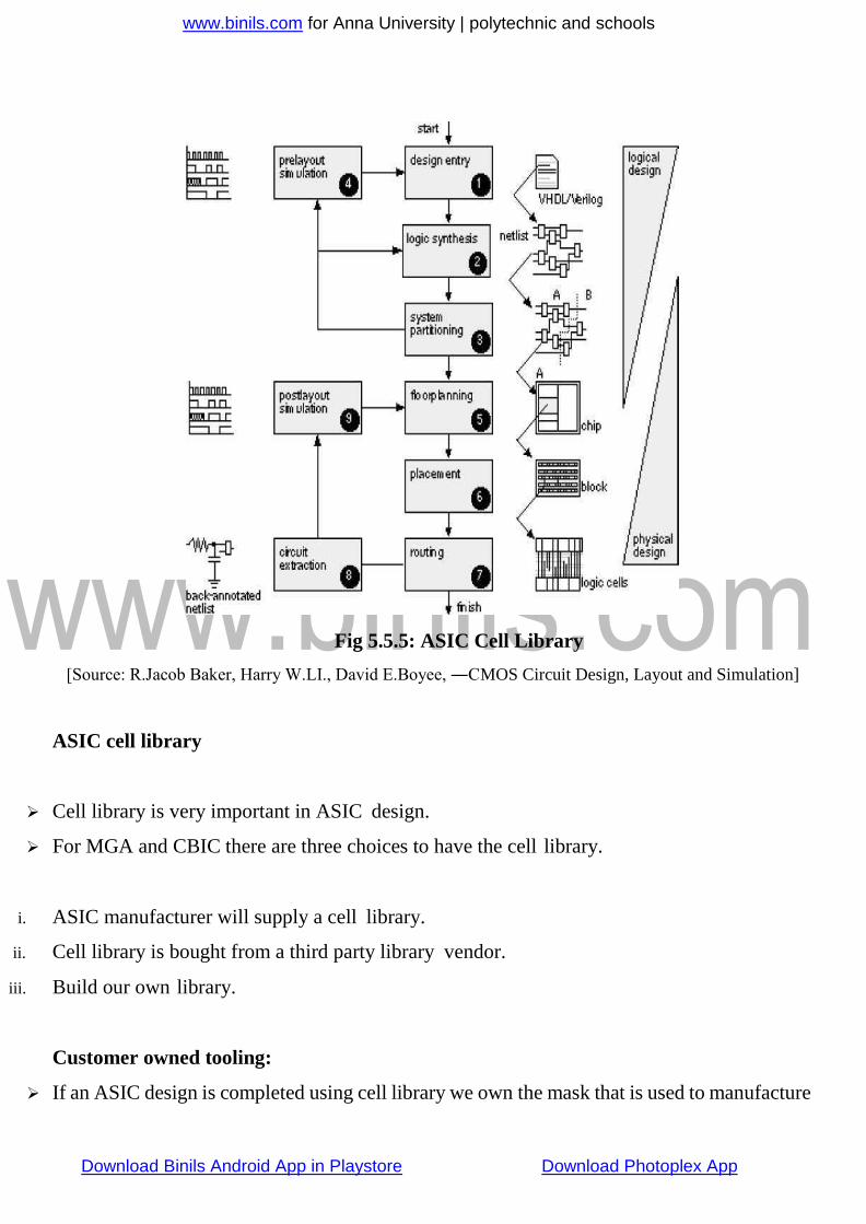
ASIC Design Flow Steps of logic design:
Step1: Design entry
Enter the design into an ASIC design systems, either using a HDL or schematic entry Step
2.Logic synthesis
Use VHDL or Verilog and a logic synthesis tool to produce a net list.
Step 3: System portioning
Divide a large system into an ASIC sized pieces.

www.binils.com for Anna University | Polytechnic and schools
Download Binils Android App in Playstore Download Photoplex App
Step 4: Pre-layout simulation
Check whether design function are correct.
Steps of physical design:
Step 5: Floor planning
Arrange the blocks of the net list on the chip.
Step 6: Placement:
Decide the locations of cells in a block.
Step 7: Routing:
Make the connections between cells and blocks.
Step 8.Extraction:
Determine the resistance and capacitance of the inter connect.
Step 9: Post layout simulation:
Check to see design still works with the added loads.
www.binils.com for Anna University | polytechnic and schools
Download Binils Android App in Playstore Download Photoplex App
Fig 5.5.5: ASIC Cell Library
[Source: R.Jacob Baker, Harry W.LI., David E.Boyee, ―CMOS Circuit Design, Layout and Simulation]
ASIC cell library
Cell library is very important in ASIC design.
For MGA and CBIC there are three choices to have the cell library.
i. ASIC manufacturer will supply a cell library.
ii. Cell library is bought from a third party library vendor.
iii. Build our own library.
Customer owned tooling:
If an ASIC design is completed using cell library we own the mask that is used to manufacture

www.binils.com for Anna University | polytechnic and schools
Download Binils Android App in Playstore Download Photoplex App
The ASIC. This is called Customer owned tooling. Each cell in an ASIC cell library contain
the following,
1. Physical layout
2. Behavioral model
3. Verilog/VHDL model
4. Timing model
5. Test strategy
6. Circuit schematic
7. Cell icon
8. Wire load model
9. Routing model
www.binils.com for Anna University | Polytechnic and schools
Download Binils Android App in Playstore Download Photoplex App
Design for Testability Techniques
Design for testability (DFT) refers to those design techniques that make the task of subsequent
testing easier. There is definitely no single methodology that solves all embedded system-
testing problems. There also is no single DFT technique, which is effective for all kinds of
circuits. DFT techniques can largely be divided into two categories, i.e., ad hoc techniques and
structured (systematic) techniques.
DFT methods for digital circuits:
Ad-hoc methods
Structured methods:
Scan
Partial Scan
Ad-hoc DFT methods
Good design practices learnt through experience are used as guidelines for ad-hoc DFT. Some
important guidelines are given below.
Things to be followed
Large circuits should be partitioned into smaller sub-circuits to reduce test costs. One of the
most important steps in designing a testable chip is to first partition the chip in an appropriate
way such that for each functional module there is an effective (DFT) technique to test it.
Partitioning must be done at every level of the design process, from architecture to circuit,
whether testing is considered or not. Partitioning can be functional (according to functional
module boundaries) or physical (based on circuit topology). Partitioning can be done by using
multiplexers and/or scan chains.
Test access points must be inserted to enhance controllability & observe ability of the circuit.
Test points include control points (CPs) and observation points (OPs). The CPs are active test
points, while the OPs are passive ones. There are also test points, which are both CPs and OPs.
www.binils.com for Anna University | Polytechnic and schools
Download Binils Android App in Playstore Download Photoplex App
Before exercising test through test points that are not PIs and POs, one should investigate into
additional requirements on the test points raised by the use of test equip mints.
Circuits (flip-flops) must be easily Initialize able to enhance predictability. A power-on reset
mechanism controllable from primary inputs is the most effective and widely used approach.
Test control must be provided for difficult-to-control signals.
Automatic Test Equipment (ATE) requirements such as pin limitation, tri-stating, timing
resolution, speed, memory depth, driving capability, analog/mixed-signal support,
internal/boundary scan support, etc., should be considered during the design process to avoid
delay of the project and unnecessary investment on the equipment’s.
Internal oscillators, PLLs and clocks should be disabled during test. To guarantee tester
synchronization, internal oscillator and clock generator circuitry should be isolated during the
test of the functional circuitry. The internal oscillators and clocks should also be tested
separately.
Analog and digital circuits should be kept physically separate. Analog circuit testing is very
much different from digital circuit testing. Testing for analog circuits refers to real
measurement, since analog signals are continuous (as opposed to discrete or logic signals in
digital circuits). They require different test equipment’s and different test methodologies.
Therefore they should be tested separately.
Things to be avoided
Asynchronous (UN clocked) logic feedback in the circuit must be avoided. A feedback in the
combinational logic can give rise to oscillation for certain inputs. Since no clocking is
employed, timing is continuous instead of discrete, which makes tester synchronization
virtually impossible, and therefore only functional test by application board can be used.
Mon stables and self-resetting logic should be avoided. A constable (one-shot) multi vibrator
produces a pulse of constant duration in response to the rising or falling transition of the trigger
input. Its pulse duration is usually controlled externally by a resistor and a capacitor (with
current technology, they also can be integrated on chip). One-shots are used

www.binils.com for Anna University | Polytechnic and schools
Download Binils Android App in Playstore Download Photoplex App
Mainly for 1) pulse shaping, 2) switch-on delays, 3) switch-off delays,
4) Signal delays. Since it is not controlled by clocks, synchronization and precise duration
control are very difficult, which in turn reduces testability by ATE. Counters and dividers are
better candidates for delay control.
Redundant gates must be avoided.
High fan in/fan out combinations must be avoided as large fan-in makes the inputs of the
gate difficult to observe and makes the gate output difficult to control.
Gated clocks should be avoided. These degrade the controllability of circuit nodes.
The above guidelines are from experienced practitioners. These are not complete or universal.
In fact, there are drawbacks for these methods:
There is a lack of experts and tools.
Test generation is often manual
This method cannot guarantee for high fault coverage.
It may increase design iterations.
This is not suitable for large circuits
Ad Hoc Testable Design Techniques
One way to increase the testability is to make nodes more accessible at some cost by
physically inserting more access circuits to the original design. Listed below are some of the
ad hoc testable design techniques.
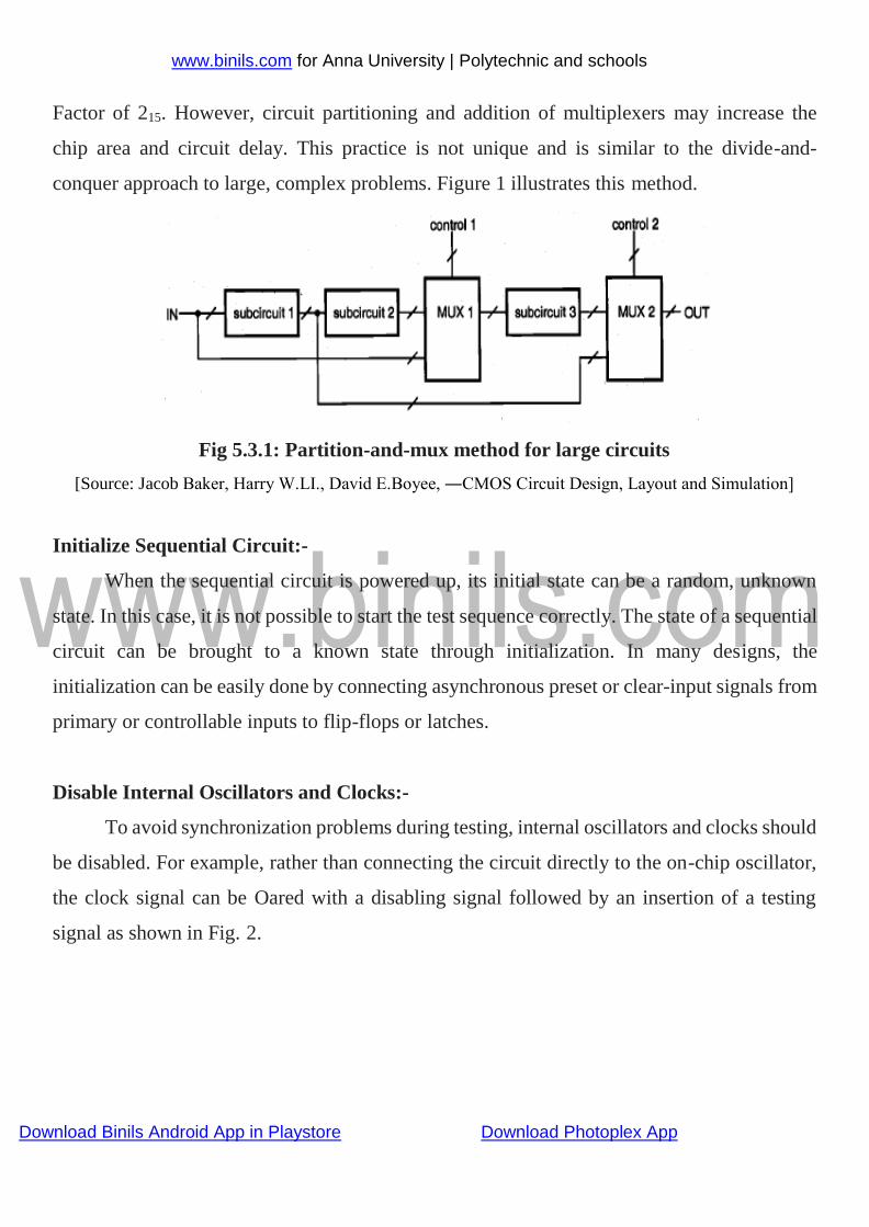
Partition-and-Mux Technique:-
Since the sequence of many serial gates, functional blocks, or large circuits are difficult
to test, such circuits can be partitioned and multiplexors (mixes) can be inserted such that
some of the primary inputs can be fed to partitioned parts through multiplexers with accessible
control signals. With this design technique, the number of accessible nodes can be increased
and the number of test patterns can be reduced. A case in point would be the 32-bit counter.
Dividing this counter into two 16-bit parts would reduce the testing time in principle by a
www.binils.com for Anna University | Polytechnic and schools
Download Binils Android App in Playstore Download Photoplex App
Factor of 215. However, circuit partitioning and addition of multiplexers may increase the
chip area and circuit delay. This practice is not unique and is similar to the divide-and-
conquer approach to large, complex problems. Figure 1 illustrates this method.
Fig 5.3.1: Partition-and-mux method for large circuits
[Source: Jacob Baker, Harry W.LI., David E.Boyee, ―CMOS Circuit Design, Layout and Simulation]
Initialize Sequential Circuit:-
When the sequential circuit is powered up, its initial state can be a random, unknown
state. In this case, it is not possible to start the test sequence correctly. The state of a sequential
circuit can be brought to a known state through initialization. In many designs, the
initialization can be easily done by connecting asynchronous preset or clear-input signals from
primary or controllable inputs to flip-flops or latches.
Disable Internal Oscillators and Clocks:-
To avoid synchronization problems during testing, internal oscillators and clocks should
be disabled. For example, rather than connecting the circuit directly to the on-chip oscillator,
the clock signal can be Oared with a disabling signal followed by an insertion of a testing
signal as shown in Fig. 2.

www.binils.com for Anna University | Polytechnic and schools
Download Binils Android App in Playstore Download Photoplex App
Fig 5.3.2: Avoid synchronization problems-via disabling of the oscillator
[Source: Jacob Baker, Harry W.LI., David E.Boyee, ―CMOS Circuit Design, Layout and Simulation]
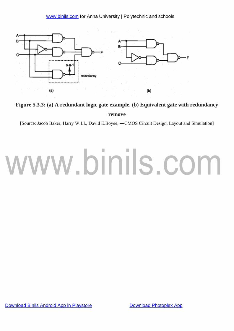
Avoid Asynchronous Logic and Redundant Logic:-
The enhancement of testability requires serious tradeoffs. The speed of an asynchronous
logic circuit can be faster than that of the synchronous logic circuit counterpart. However, the
design and test of an asynchronous logic circuit are more difficult than for a synchronous logic
circuit, and its state transition times are difficult to predict. Also, the operation of an
asynchronous logic circuit is sensitive to input test patterns, often causing race problems and
hazards of having momentary signal values opposite to the expected values. Sometimes,
designed-in logic redundancy is used to mask a static hazard condition for reliability. However,
the redundant node cannot be observed since the primary output value cannot be made
dependent on the value of the redundant node. Hence, certain faults on the redundant node
cannot be tested or detected. Figure 3 shows that the bottom NAND2 gate is redundant and
the stuck-at- fault on its output line cannot be detected. If a fault is undetectable, the associated
line or gate can be removed without changing the logic function.
www.binils.com for Anna University | Polytechnic and schools
Download Binils Android App in Playstore Download Photoplex App
Figure 5.3.3: (a) A redundant logic gate example. (b) Equivalent gate with redundancy
remove
[Source: Jacob Baker, Harry W.LI., David E.Boyee, ―CMOS Circuit Design, Layout and Simulation]
www.binils.com for Anna University | Polytechnic and schools
Download Binils Android App in Playstore Download Photoplex App
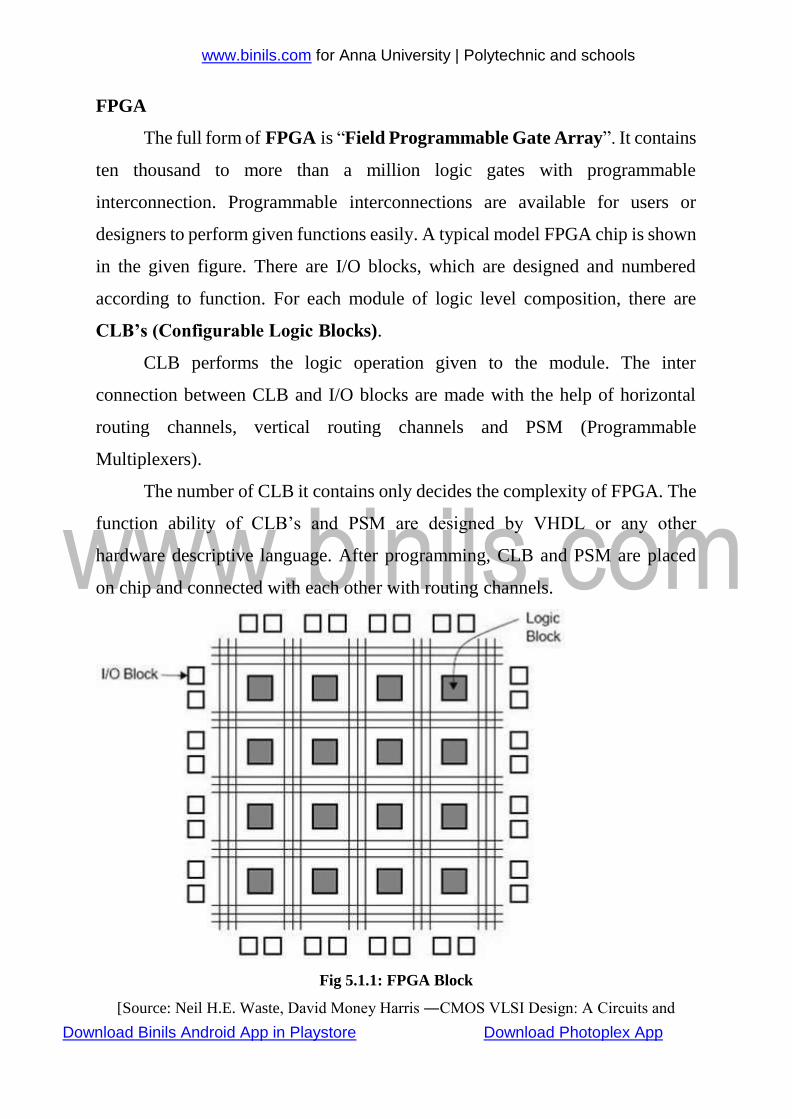
FPGA
The full form of FPGA is “Field Programmable Gate Array”. It contains
ten thousand to more than a million logic gates with programmable
interconnection. Programmable interconnections are available for users or
designers to perform given functions easily. A typical model FPGA chip is shown
in the given figure. There are I/O blocks, which are designed and numbered
according to function. For each module of logic level composition, there are
CLB’s (Configurable Logic Blocks).
CLB performs the logic operation given to the module. The inter
connection between CLB and I/O blocks are made with the help of horizontal
routing channels, vertical routing channels and PSM (Programmable
Multiplexers).
The number of CLB it contains only decides the complexity of FPGA. The
function ability of CLB’s and PSM are designed by VHDL or any other
hardware descriptive language. After programming, CLB and PSM are placed
on chip and connected with each other with routing channels.
Fig 5.1.1: FPGA Block
[Source: Neil H.E. Waste, David Money Harris ―CMOS VLSI Design: A Circuits and
www.binils.com for Anna University | Polytechnic and schools
Download Binils Android App in Playstore Download Photoplex App
Systems Perspective]
Advantages
It requires very small time; starting from design process to functional chip.
No physical manufacturing steps are involved in it.
The only disadvantage is, it is costly than other styles.
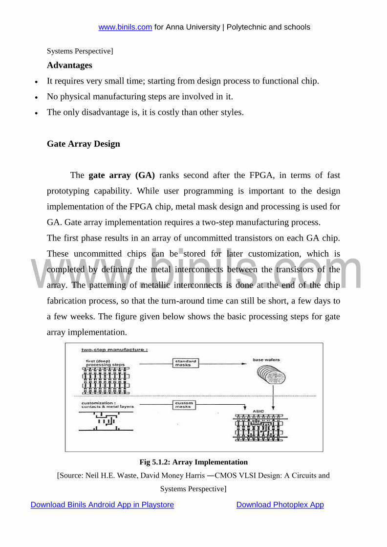
Gate Array Design
The gate array (GA) ranks second after the FPGA, in terms of fast
prototyping capability. While user programming is important to the design
implementation of the FPGA chip, metal mask design and processing is used for
GA. Gate array implementation requires a two-step manufacturing process.
The first phase results in an array of uncommitted transistors on each GA chip.
These uncommitted chips can be stored for later customization, which is
completed by defining the metal interconnects between the transistors of the
array. The patterning of metallic interconnects is done at the end of the chip
fabrication process, so that the turn-around time can still be short, a few days to
a few weeks. The figure given below shows the basic processing steps for gate
array implementation.
Fig 5.1.2: Array Implementation
[Source: Neil H.E. Waste, David Money Harris ―CMOS VLSI Design: A Circuits and
Systems Perspective]
www.binils.com for Anna University | Polytechnic and schools
Download Binils Android App in Playstore Download Photoplex App
Typical gate array platforms use dedicated areas called channels, for inter-cell
routing between rows or columns of MOS transistors. They simplify the
interconnections. Interconnection patterns that perform basic logic gates are
stored in a library, which can then be used to customize rows of uncommitted
transistors according to the net list.
In most of the modern GAs, multiple metal layers are used for channel
routing. With the use of multiple interconnected layers, the routing can be
achieved over the active cell areas; so that the routing channels can be removed
as in Sea-of-Gates (SOG) chips. Here, the entire chip surface is covered with
uncommitted names and props transistors. The neighboring transistors can be
customized using a metal mask to form basic logic gates.
For inter cell routing, some of the uncommitted transistors must be
sacrificed. This design style results in more flexibility for interconnections and
usually in a higher density. GA chip utilization factor is measured by the used
chip area divided by the total chip area. It is higher than that of the FPGA and so
is the chip speed.
Standard Cell Based Design
A standard cell based design requires development of a full custom mask
set. The standard cell is also known as the police. In this approach, all of the
commonly used logic cells are developed, characterized and stored in a standard
cell library.
A library may contain a few hundred cells including inverters, NAND
gates, NOR gates, complex AOI, OAI gates, D-latches and Flip-flops. Each gate
type can be implemented in several versions to provide adequate driving
capability for different fan-outs. The inverter gate can have standard size, double
www.binils.com for Anna University | Polytechnic and schools
Download Binils Android App in Playstore Download Photoplex App
Size, and quadruple size so that the chip designer can select the proper size to
obtain high circuit speed and layout density.
Each cell is characterized according to several different characterization
categories, such as,
Delay time versus load capacitance
Circuit simulation model
Timing simulation model
Fault simulation model
Cell data for place-and-route
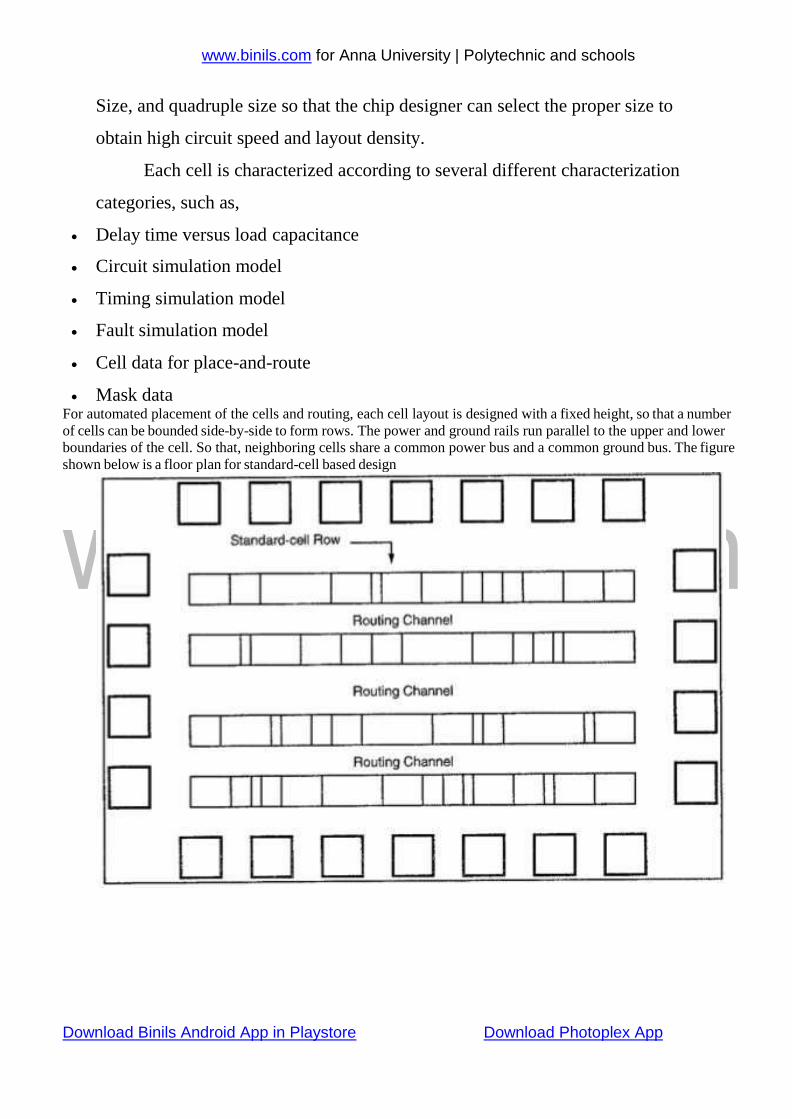
Mask data For automated placement of the cells and routing, each cell layout is designed with a fixed height, so that a number
of cells can be bounded side-by-side to form rows. The power and ground rails run parallel to the upper and lower
boundaries of the cell. So that, neighboring cells share a common power bus and a common ground bus. The figure
shown below is a floor plan for standard-cell based design
www.binils.com for Anna University | Polytechnic and schools
Download Binils Android App in Playstore Download Photoplex App
Fig 5.1.3: Floor plan For Standard-Cell Based Design
[Source: Neil H.E. Waste, David Money Harris ―CMOS VLSI Design: A Circuits and
Systems Perspective]
Full Custom Design
In a full-custom design, the entire mask design is made new, without the
use of any library. The development cost of this design style is rising. Thus, the
concept of design reuse is becoming famous to reduce design cycle time and
development cost.
The hardest full custom design can be the design of a memory cell, be it
static or dynamic. For logic chip design, a good negotiation can be obtained using
a combination of different design styles on the same chip, i.e. standard cells, data-
path cells, and programmable logic arrays (PLAs).
Practically, the designer does the full custom layout, i.e. the geometry,
orientation, and placement of every transistor. The design productivity is usually
very low; typically a few tens of transistors per day, per designer. In digital
CMOS VLSI, full-custom design is hardly used due to the high labor cost. These
design styles include the design of high-volume products such as memory chips,
high-performance microprocessors and FPGA.
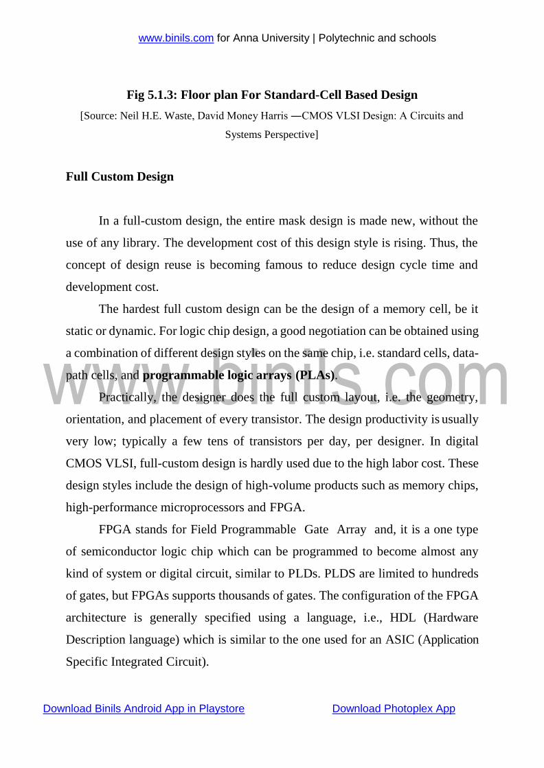
FPGA stands for Field Programmable Gate Array and, it is a one type
of semiconductor logic chip which can be programmed to become almost any
kind of system or digital circuit, similar to PLDs. PLDS are limited to hundreds
of gates, but FPGAs supports thousands of gates. The configuration of the FPGA
architecture is generally specified using a language, i.e., HDL (Hardware
Description language) which is similar to the one used for an ASIC (Application
Specific Integrated Circuit).
www.binils.com for Anna University | Polytechnic and schools
Download Binils Android App in Playstore Download Photoplex App
Fig 5.1.4: FPGA
[Source: Neil H.E. Waste, David Money Harris ―CMOS VLSI Design: A Circuits and
Systems Perspective]
FPGAs can provide a number of advantages over a fixed function ASIC
technology such as standard cells. Normally, ASICs takes months to manufacture
and the cost of them will be thousands of dollars to obtain the device. But FPGAs
are fabricated in less than a second, the cost will be from a few dollars to a
thousand dollars. The flexible nature of the FPGA comes at a significant costing
area, power consumption and delay. When compared to a standard cell ASIC, an
FPGA requires 20 to 35 times more area, and the speed’s performance will be 3
to 4 times slower than the ASIC. This article describes about the FPGA basics
and FPGA architecture module that includes I/O pad, logic blocks and switch
matrix. FPGAs are some of the new trending areas of VLSI.
FPGA Architecture
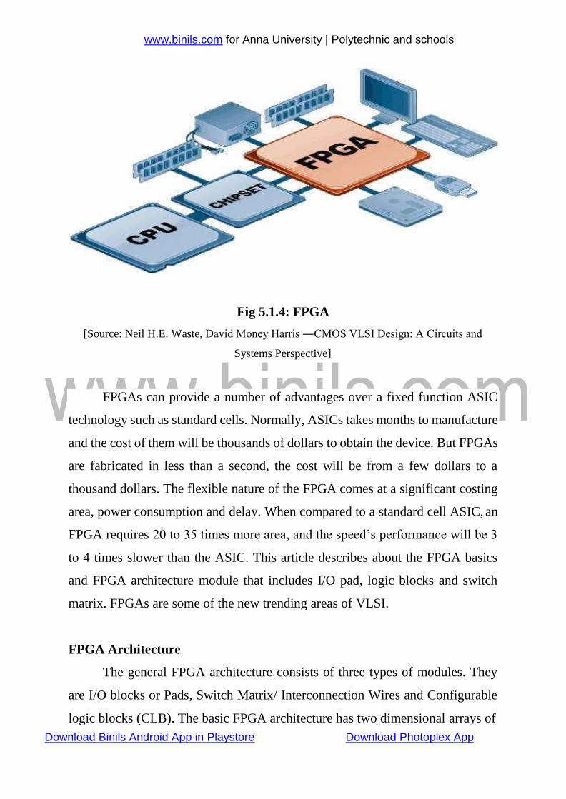
The general FPGA architecture consists of three types of modules. They
are I/O blocks or Pads, Switch Matrix/ Interconnection Wires and Configurable
logic blocks (CLB). The basic FPGA architecture has two dimensional arrays of
www.binils.com for Anna University | Polytechnic and schools
Download Binils Android App in Playstore Download Photoplex App
Logic.
Depending on the logic, switch matrix provides switching between interconnects.
I/O Pads used for the outside world to communicate with different applications.
Logic blocks with a means for a user to arrange the interconnection between the
logic blocks. The functions of an FPGA architecture module are discussed below:
CLB (Configurable Logic Block) includes digital logic, inputs, and outputs. It
implements the user logic.
Interconnects provide direction between the logic blocks to implement the user
Fig 5.1.5: FPGA Block
[Source: Neil H.E. Waste, David Money Harris ―CMOS VLSI Design: A Circuits and
Systems Perspective]
FPGA Architecture
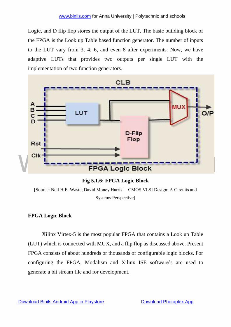
Logic Block contains MUX (Multiplexer), D flip flop and LUT. LUT
implements the combinational logical functions; the MUX is used for selection
www.binils.com for Anna University | Polytechnic and schools
Download Binils Android App in Playstore Download Photoplex App
Logic, and D flip flop stores the output of the LUT. The basic building block of
the FPGA is the Look up Table based function generator. The number of inputs
to the LUT vary from 3, 4, 6, and even 8 after experiments. Now, we have
adaptive LUTs that provides two outputs per single LUT with the
implementation of two function generators.
Fig 5.1.6: FPGA Logic Block
[Source: Neil H.E. Waste, David Money Harris ―CMOS VLSI Design: A Circuits and
Systems Perspective]
FPGA Logic Block
Xilinx Virtex-5 is the most popular FPGA that contains a Look up Table
(LUT) which is connected with MUX, and a flip flop as discussed above. Present
FPGA consists of about hundreds or thousands of configurable logic blocks. For
configuring the FPGA, Modalism and Xilinx ISE software’s are used to
generate a bit stream file and for development.
www.binils.com for Anna University | Polytechnic and schools
Download Binils Android App in Playstore Download Photoplex App
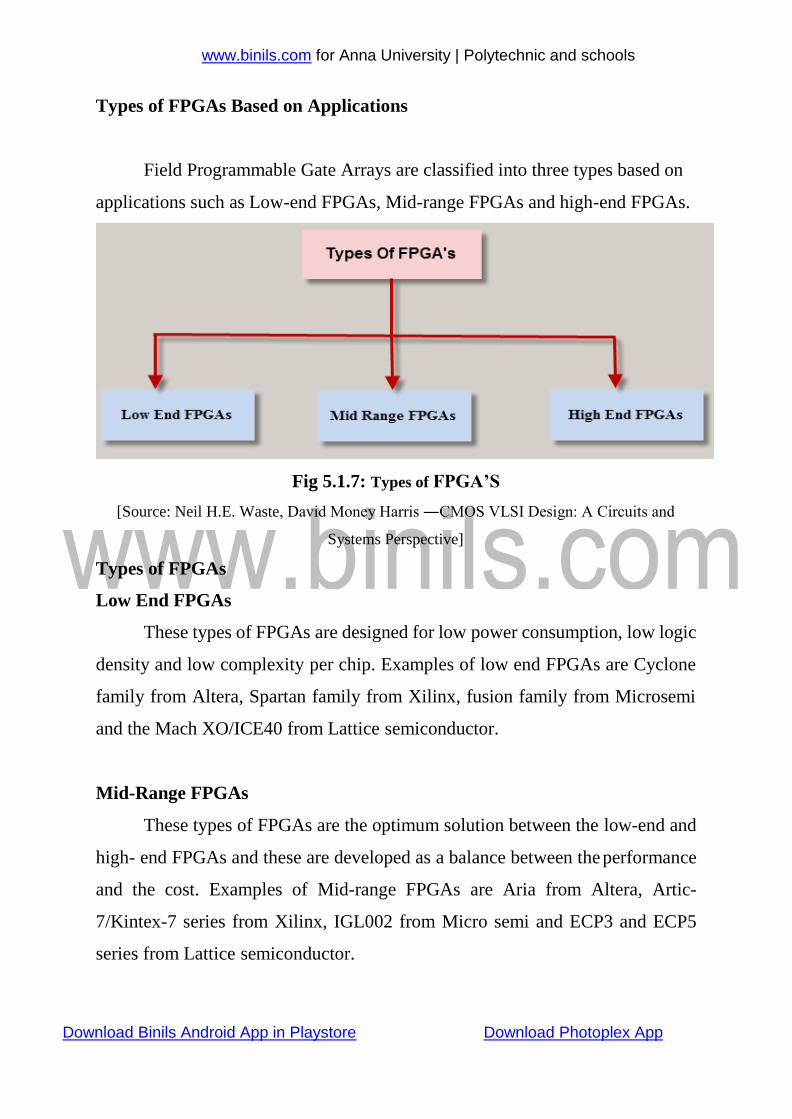
Types of FPGAs Based on Applications
Field Programmable Gate Arrays are classified into three types based on
applications such as Low-end FPGAs, Mid-range FPGAs and high-end FPGAs.
Fig 5.1.7: Types of FPGA’S
[Source: Neil H.E. Waste, David Money Harris ―CMOS VLSI Design: A Circuits and
Systems Perspective]
Types of FPGAs
Low End FPGAs
These types of FPGAs are designed for low power consumption, low logic
density and low complexity per chip. Examples of low end FPGAs are Cyclone
family from Altera, Spartan family from Xilinx, fusion family from Microsemi
and the Mach XO/ICE40 from Lattice semiconductor.
Mid-Range FPGAs
These types of FPGAs are the optimum solution between the low-end and
high- end FPGAs and these are developed as a balance between the performance
and the cost. Examples of Mid-range FPGAs are Aria from Altera, Artic-
7/Kintex-7 series from Xilinx, IGL002 from Micro semi and ECP3 and ECP5
series from Lattice semiconductor.
www.binils.com for Anna University | Polytechnic and schools
Download Binils Android App in Playstore Download Photoplex App
High End FPGAs
These types of FPGAs are developed for logic density and high
performance. Examples of High end FPGAs are a Strati family from Altera,
Vertex family from Xilinx, Speedster 22i family from Chronic, and ProASIC3
family from Micro semi.
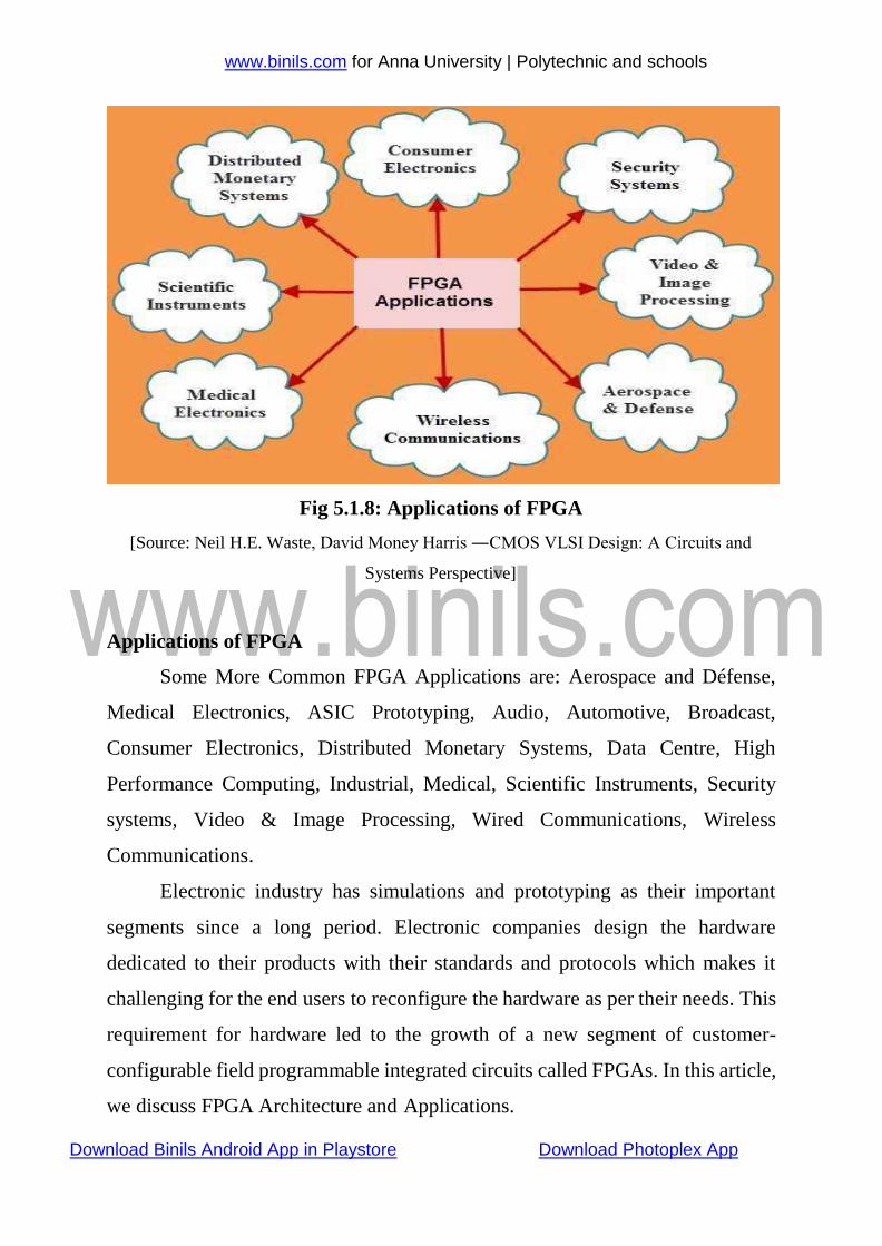
Applications of FPGA:
FPGAs have gained rapid growth over the past decade because they are
useful for a wide range of applications. Specific application of an FPGA includes
digital signal processing, bioinformatics, device controllers, software-defined
radio, random logic, ASIC prototyping, medical imaging, computer hardware
emulation, integrating multiple SPLDs, voice recognition, cryptography, filtering
and communication encoding and many more.
Usually, FPGAs are kept for particular vertical applications where the production
volume is small. For these low-volume applications, the top companies pay in
hardware costs per unit. Today, the new performance dynamics and cost have
extended the range of viable applications.
www.binils.com for Anna University | Polytechnic and schools
Download Binils Android App in Playstore Download Photoplex App
Fig 5.1.8: Applications of FPGA
[Source: Neil H.E. Waste, David Money Harris ―CMOS VLSI Design: A Circuits and
Systems Perspective]
Applications of FPGA
Some More Common FPGA Applications are: Aerospace and Défense,
Medical Electronics, ASIC Prototyping, Audio, Automotive, Broadcast,
Consumer Electronics, Distributed Monetary Systems, Data Centre, High
Performance Computing, Industrial, Medical, Scientific Instruments, Security
systems, Video & Image Processing, Wired Communications, Wireless
Communications.
Electronic industry has simulations and prototyping as their important
segments since a long period. Electronic companies design the hardware
dedicated to their products with their standards and protocols which makes it
challenging for the end users to reconfigure the hardware as per their needs. This
requirement for hardware led to the growth of a new segment of customer-
configurable field programmable integrated circuits called FPGAs. In this article,
we discuss FPGA Architecture and Applications.
www.binils.com for Anna University | Polytechnic and schools
Download Binils Android App in Playstore Download Photoplex App
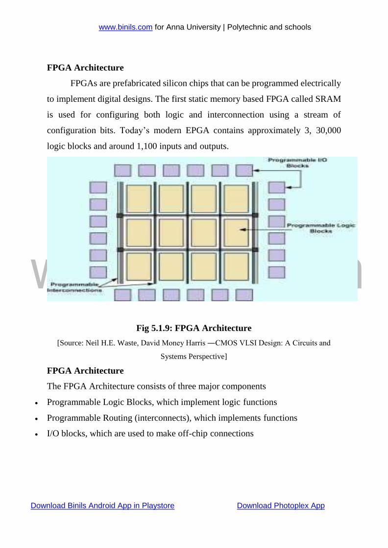
FPGA Architecture
FPGAs are prefabricated silicon chips that can be programmed electrically
to implement digital designs. The first static memory based FPGA called SRAM
is used for configuring both logic and interconnection using a stream of
configuration bits. Today’s modern EPGA contains approximately 3, 30,000
logic blocks and around 1,100 inputs and outputs.
Fig 5.1.9: FPGA Architecture
[Source: Neil H.E. Waste, David Money Harris ―CMOS VLSI Design: A Circuits and
Systems Perspective]
FPGA Architecture
The FPGA Architecture consists of three major components
Programmable Logic Blocks, which implement logic functions
Programmable Routing (interconnects), which implements functions
I/O blocks, which are used to make off-chip connections
www.binils.com for Anna University | Polytechnic and schools
Download Binils Android App in Playstore Download Photoplex App
Programmable Logic Blocks
The programmable logic block provides basic computation and storage
elements used in digital systems. A basic logic element consists of programmable
combinational logic, a flip-flop, and some fast carry logic to reduce area and delay
cost.
Modern FPGAs contain a heterogeneous mixture of different blocks like
dedicated memory blocks, multiplexers. Configuration memory is used
throughout the logic blocks to control the specific function of each element.
Programmable Routing
The programmable routing establishes a connection between logic blocks
and Input/output blocks to complete a user-defined design unit.
It consists of multiplexers pass transistors and tri-state buffers. Pass transistors
and multiplexers are used in a logic cluster to connect the logic elements.
Programmable I/O
The programmable I/O pads are used to interface the logic blocks and
routing architecture to the external components. The I/O pad and the surrounding
logic circuit form as an I/O cell.
These cells consume a large portion of the FPGA’s area. And the design of
I/O programmable blocks is complex, as there are great differences in the supply
voltage and reference voltage. The selection of standards is important in I/O
architecture design. Supporting a large number of standards can increase the
silicon chip area required for I/O cells. With advancement, the basic FPGA
Architecture has developed through the addition of more specialized
programmable function blocks. The special functional blocks like ALUs, block
RAM, multiplexers, DSP-48, and microprocessors have been added to the FPGA,
due to the frequency of the need for such resources for applications.
www.binils.com for Anna University | Polytechnic and schools
Download Binils Android App in Playstore Download Photoplex App
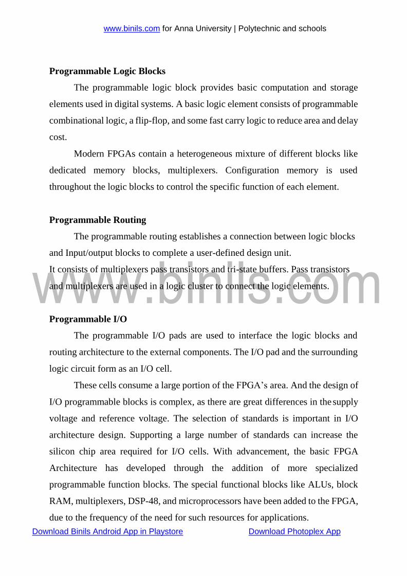
The below snap shows an example of an FPGA Board.
Fig 5.1.10: FPGA Board
[Source: Neil H.E. Waste, David Money Harris ―CMOS VLSI Design: A Circuits and
Systems Perspective]
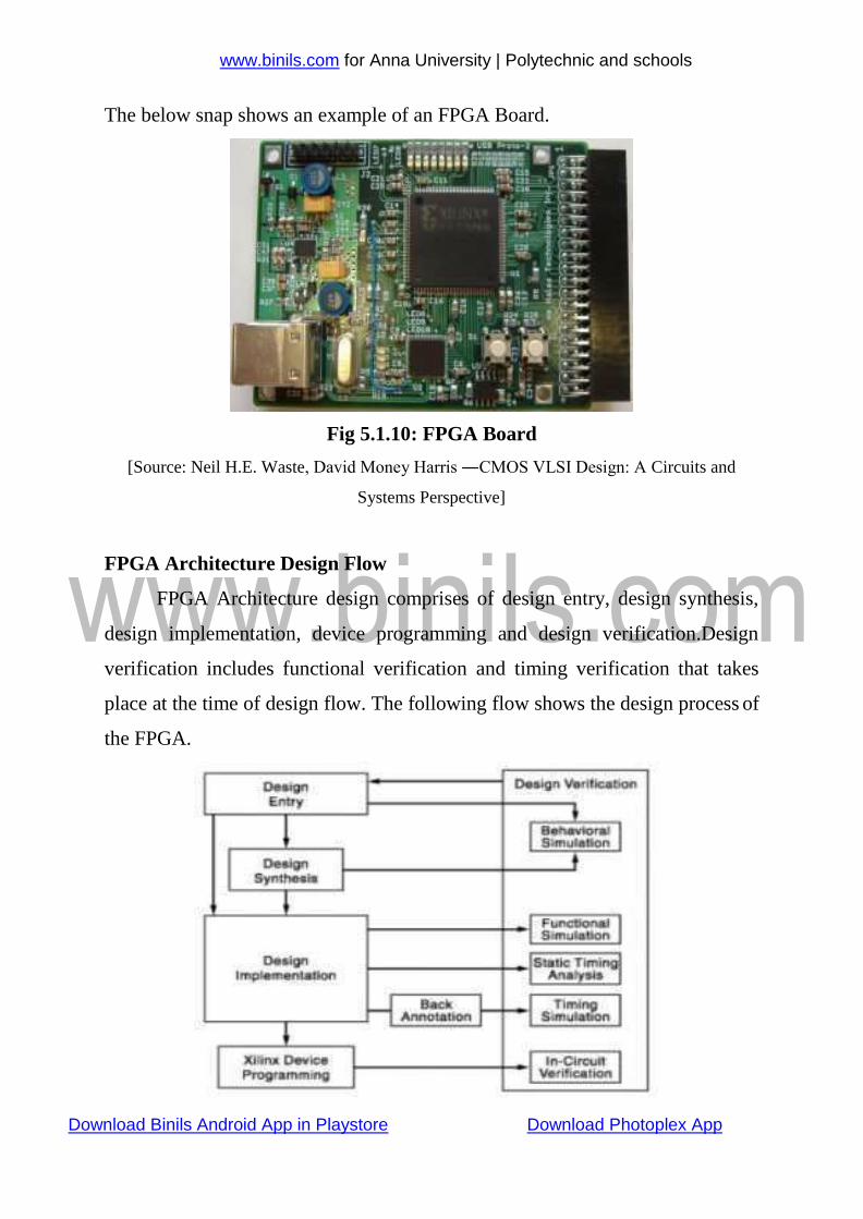
FPGA Architecture Design Flow
FPGA Architecture design comprises of design entry, design synthesis,
design implementation, device programming and design verification.Design
verification includes functional verification and timing verification that takes
place at the time of design flow. The following flow shows the design process of
the FPGA.

www.binils.com for Anna University | Polytechnic and schools
Download Binils Android App in Playstore Download Photoplex App
Fig 5.1.11: FPGA Architecture Design Flow
[Source: Neil H.E. Waste, David Money Harris ―CMOS VLSI Design: A Circuits and
Systems Perspective]
Design Entry
The design entry is done in different techniques like schematic based,
hardware description language (HDL) and a combination of both etc. If the
designer wants to deal with hardware, then the schematic entry is a good choice.
If the designer thinks the design in an algorithmic way, then the HDL is the better
choice. The schematic based entry gives the designer a greater visibility and
control over the hardware.
Design Synthesis
This process translates VHDL code into a device net list format, i.e., a
complete circuit with logical elements. The design synthesis process will check
the code syntax and analyze the hierarchy of the design architecture.
This ensures the design optimized for the design architecture. The net list is
saved as Native Generic Circuit (NGC) file.
Design Implementation
The implementation process consists of
Translate
Map
Place and Route
Translate
This process combines all the input net lists to the logic design file which
is saved as NGD (Native Generic Database) file. Here the ports are assigned to
the physical elements like pins, switches in the design. This is stored in a file
called User Constraints File (UCF).
www.binils.com for Anna University | Polytechnic and schools
Download Binils Android App in Playstore Download Photoplex App
Fig 5.1.12: Translate
[Source: Neil H.E. Waste, David Money Harris ―CMOS VLSI Design: A Circuits and
Systems Perspective]
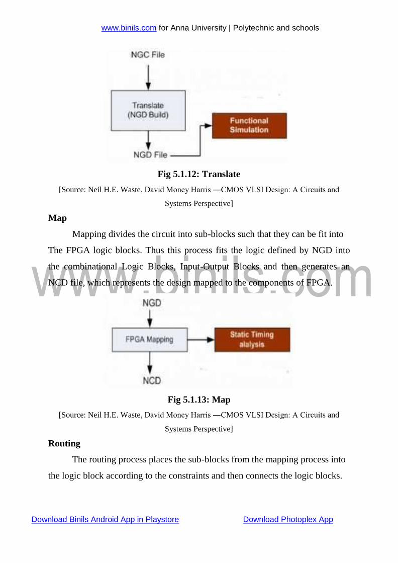
Map
Mapping divides the circuit into sub-blocks such that they can be fit into
The FPGA logic blocks. Thus this process fits the logic defined by NGD into
the combinational Logic Blocks, Input-Output Blocks and then generates an
NCD file, which represents the design mapped to the components of FPGA.
Fig 5.1.13: Map
[Source: Neil H.E. Waste, David Money Harris ―CMOS VLSI Design: A Circuits and
Systems Perspective]
Routing
The routing process places the sub-blocks from the mapping process into
the logic block according to the constraints and then connects the logic blocks.
www.binils.com for Anna University | Polytechnic and schools
Download Binils Android App in Playstore Download Photoplex App
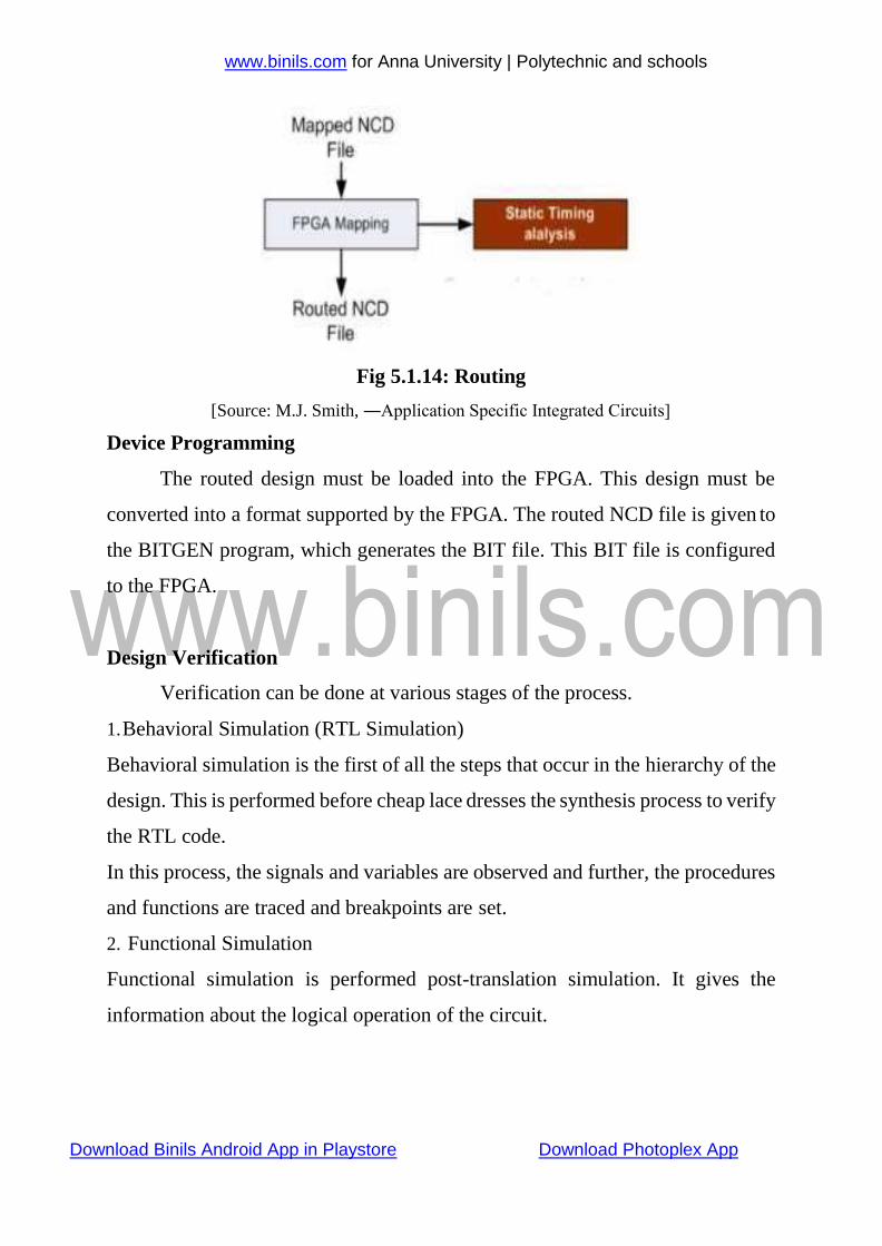
Fig 5.1.14: Routing
[Source: M.J. Smith, ―Application Specific Integrated Circuits]
Device Programming
The routed design must be loaded into the FPGA. This design must be
converted into a format supported by the FPGA. The routed NCD file is given to
the BITGEN program, which generates the BIT file. This BIT file is configured
to the FPGA.
Design Verification
Verification can be done at various stages of the process.
1. Behavioral Simulation (RTL Simulation)
Behavioral simulation is the first of all the steps that occur in the hierarchy of the
design. This is performed before cheap lace dresses the synthesis process to verify
the RTL code.
In this process, the signals and variables are observed and further, the procedures
and functions are traced and breakpoints are set.
2. Functional Simulation
Functional simulation is performed post-translation simulation. It gives the
information about the logical operation of the circuit.
www.binils.com for Anna University | Polytechnic and schools
Download Binils Android App in Playstore Download Photoplex App
3. Static Timing Simulation
This is done post mapping. Post map timing report gives the signal path delays.
After place and route, timing report takes the timing delay information. This
provides a complete timing summary of the design.
Applications of FPGA
FPGAs have gained a quick acceptance over the past decades. Here are the some
of the applications of FPGAs in various technologies.
Users can apply them to the wide range of applications like random logics,
SPLDs, device controllers, communication encoding and filtering.
The emulation of e n t i r e large hardware systems via the use of many
interconnected FPGAs.
They offer a powerful solution for meeting machine vision, industrial networking,
motor control and video surveillance.
FPGAs are used in custom computing machines.
FPGAs provide a unique combination of highly parallel custom computation and
low-cost computation.
Download Binils Android App in Playstore Download Photoplex App
www.binils.com for Anna University | Polytechnic and schools
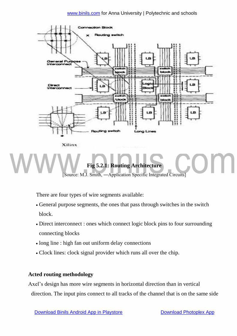
FPGA Routing Procedure
A wire segment can be described as two end points of an interconnect with no
programmable switch between them. A sequence of one or more wire segments in
an FPGA can be termed as a track. Typically an FPGA has logic blocks,
interconnects and Input/output blocks. Input Output blocks lie in the periphery of
logic blocks and interconnect. Wire segments connect I/O blocks to wire segments
through connection blocks. Connection blocks are connected to logic blocks,
depending on the design requirement one logic block is connected to another and so
on.
Xilinx Routing architecture
In Xilinx routing, connections are made from logic block into the channel
through a connection block. As SRAM technology is used to implement Lookup
Tables, connection sites are large. A logic block is surrounded by connection blocks
on all four sides. They connect logic block pins to wire segments. Pass transistors
are used to implement connection for output pins, while use of multiplexers for input
pins saves the number of SRAM cells required per pin. The logic block pins
connecting to connection blocks can then be connected to any number of wire
segments through switching blocks.
Download Binils Android App in Playstore Download Photoplex App
www.binils.com for Anna University | Polytechnic and schools
Fig 5.2.1: Routing Architecture
[Source: M.J. Smith, ―Application Specific Integrated Circuits]
There are four types of wire segments available:
General purpose segments, the ones that pass through switches in the switch
block.
Direct interconnect : ones which connect logic block pins to four surrounding
connecting blocks
long line : high fan out uniform delay connections
Clock lines: clock signal provider which runs all over the chip.
Acted routing methodology
Axel’s design has more wire segments in horizontal direction than in vertical
direction. The input pins connect to all tracks of the channel that is on the same side
Download Binils Android App in Playstore Download Photoplex App
www.binils.com for Anna University | Polytechnic and schools
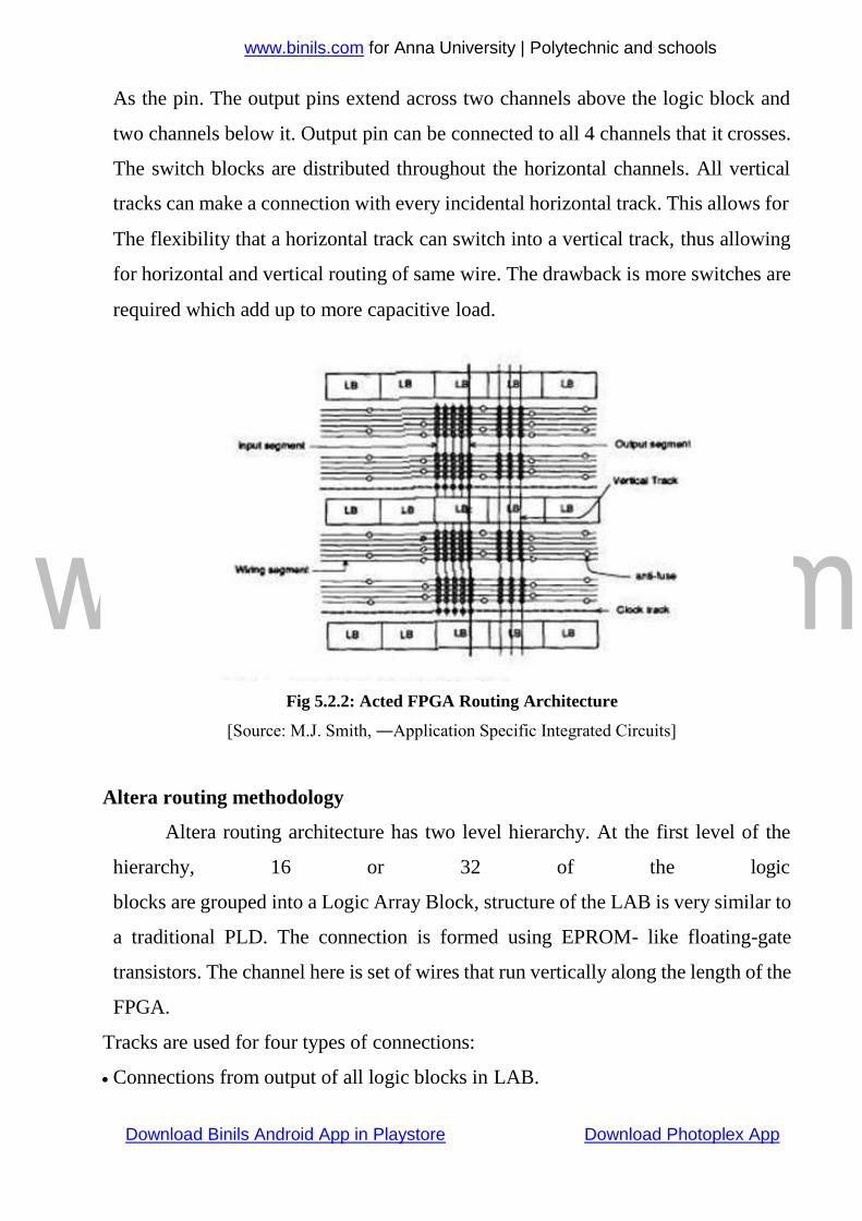
As the pin. The output pins extend across two channels above the logic block and
two channels below it. Output pin can be connected to all 4 channels that it crosses.
The switch blocks are distributed throughout the horizontal channels. All vertical
tracks can make a connection with every incidental horizontal track. This allows for
Fig 5.2.2: Acted FPGA Routing Architecture
[Source: M.J. Smith, ―Application Specific Integrated Circuits]
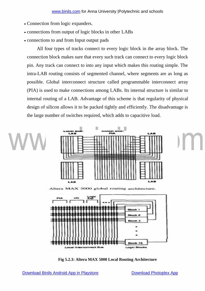
Altera routing methodology
Altera routing architecture has two level hierarchy. At the first level of the
hierarchy, 16 or 32 of the logic
blocks are grouped into a Logic Array Block, structure of the LAB is very similar to
a traditional PLD. The connection is formed using EPROM- like floating-gate
transistors. The channel here is set of wires that run vertically along the length of the
FPGA.
Tracks are used for four types of connections:
Connections from output of all logic blocks in LAB.
The flexibility that a horizontal track can switch into a vertical track, thus allowing
for horizontal and vertical routing of same wire. The drawback is more switches are
required which add up to more capacitive load.
Download Binils Android App in Playstore Download Photoplex App
www.binils.com for Anna University |Polytechnic and schools
Connection from logic expanders.
connections from output of logic blocks in other LABs
connections to and from Input output pads
All four types of tracks connect to every logic block in the array block. The
connection block makes sure that every such track can connect to every logic block
pin. Any track can connect to into any input which makes this routing simple. The
intra-LAB routing consists of segmented channel, where segments are as long as
possible. Global interconnect structure called programmable interconnect array
(PIA) is used to make connections among LABs. Its internal structure is similar to
internal routing of a LAB. Advantage of this scheme is that regularity of physical
design of silicon allows it to be packed tightly and efficiently. The disadvantage is
the large number of switches required, which adds to capacitive load.
Fig 5.2.3: Altera MAX 5000 Local Routing Architecture
Download Binils Android App in Playstore Download Photoplex App
www.binils.com for Anna University |Polytechnic and schools
[Source: M.J. Smith, ―Application Specific Integrated Circuits]
FPGA has different types of programmable interconnect. The structure and
complexity of interconnect is determined by programming technology and
architecture of basic logic cell. The raw material used to build interconnect is
aluminum based metallization with sheet resistance. Programmable ASIC comes
with two layers, three layers or more layers of metal interconnect.
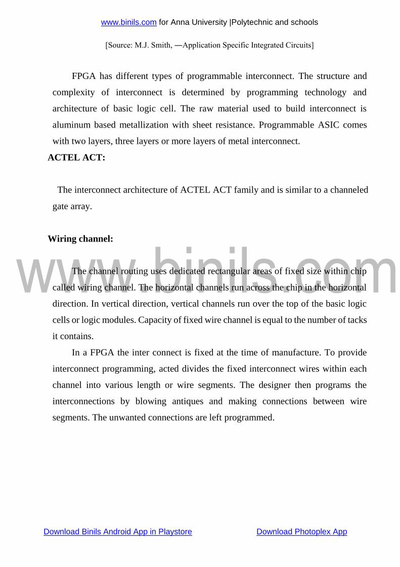
ACTEL ACT:
The interconnect architecture of ACTEL ACT family and is similar to a channeled
gate array.
Wiring channel:
The channel routing uses dedicated rectangular areas of fixed size within chip
called wiring channel. The horizontal channels run across the chip in the horizontal
direction. In vertical direction, vertical channels run over the top of the basic logic
cells or logic modules. Capacity of fixed wire channel is equal to the number of tacks
it contains.
In a FPGA the inter connect is fixed at the time of manufacture. To provide
interconnect programming, acted divides the fixed interconnect wires within each
channel into various length or wire segments. The designer then programs the
interconnections by blowing antiques and making connections between wire
segments. The unwanted connections are left programmed.
Download Binils Android App in Playstore Download Photoplex App
www.binils.com for Anna University | Polytechnic and schools
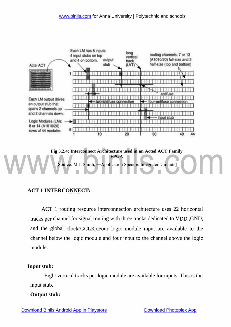
Fig 5.2.4: Interconnect Architecture used in an Acted ACT Family
FPGA
[Source: M.J. Smith, ―Application Specific Integrated Circuits]
ACT 1 INTERCONNECT:
ACT 1 routing resource interconnection architecture uses 22 horizontal
tracks per channel for signal routing with three tracks dedicated to VDD ,GND,
and the global clock(GCLK).Four logic module input are available to the
channel below the logic module and four input to the channel above the logic
module.
Input stub:
Eight vertical tracks per logic module are available for inputs. This is the
input stub.
Output stub:
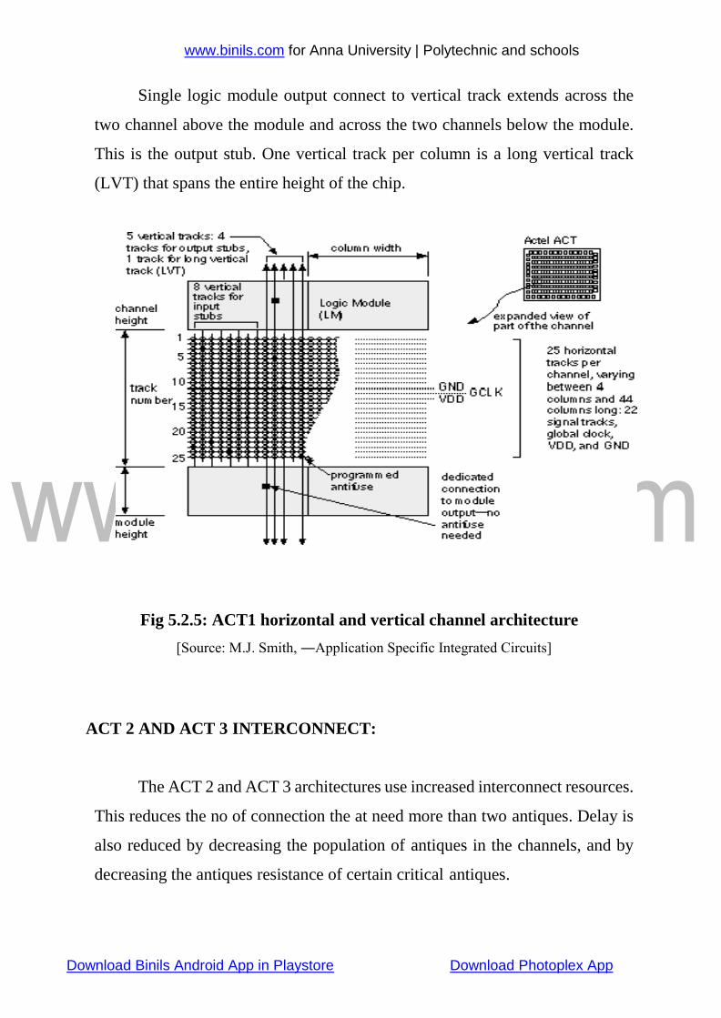
Download Binils Android App in Playstore Download Photoplex App
www.binils.com for Anna University | Polytechnic and schools
Single logic module output connect to vertical track extends across the
two channel above the module and across the two channels below the module.
This is the output stub. One vertical track per column is a long vertical track
(LVT) that spans the entire height of the chip.
Fig 5.2.5: ACT1 horizontal and vertical channel architecture
[Source: M.J. Smith, ―Application Specific Integrated Circuits]
ACT 2 AND ACT 3 INTERCONNECT:
The ACT 2 and ACT 3 architectures use increased interconnect resources.
This reduces the no of connection the at need more than two antiques. Delay is
also reduced by decreasing the population of antiques in the channels, and by
decreasing the antiques resistance of certain critical antiques.
Download Binils Android App in Playstore Download Photoplex App
www.binils.com for Anna University | Polytechnic and schools
Channel density:
It is the absolute minimum no of tracks needed in a channel to make given
set of connection. The ACT 2/3 logic modules need an extra two vertical tracks
per channel. The ACT 2/3 logic modules can accept five input, rather than four
input for the ACT1 modules. The number of tracks per column increases from
13 to 15 in the ACT 2 architecture. The greatest challenge facing the ACTEL
FPGA architecture is the resistance of poly silicon antiques.
XILINX LCA:
XILINX LCA basic logic cells are called the configurable logic block or
CLB.
CLB’s are bigger and more complex than the ACTEL logic cells. Xilinx LCA
uses coarse gain architecture. Xilinx CLB contain both combinational logic and
flip flops.
XC 3000 CLB:
XC 3000 CLB which has five logic inputs. A common clock input, an
asynchronous direct rest input and an enable. Two CLB outputs X and Y are
connected independently to the Flip-flop output QX and QY or to the
combinational logic F and G using programmable MUX connected to the
SRAM programming cells. To implement five input AND, F=A.B.C.D.E,set
LUT cell number 31 with address “11111”in the 32 bit SRAM to “1”.Since 32
bit LUT needs five variables to form unique address 32=25
XC 4000 LOGIC BLOCK:
This is a complicated basic logic cell containing 2 four input LUT’S that
feed
a three input LUT. This has special fast carry logic hardwired between CLB’S
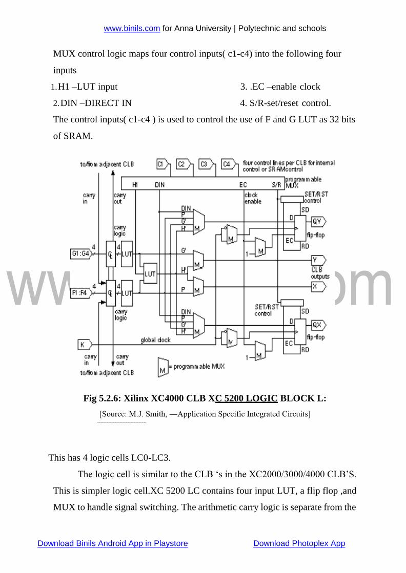
Download Binils Android App in Playstore Download Photoplex App
www.binils.com for Anna University | Polytechnic and schools
MUX control logic maps four control inputs( c1-c4) into the following four
inputs
1. H1 –LUT input 3. .EC –enable clock
2. DIN –DIRECT IN 4. S/R-set/reset control.
The control inputs( c1-c4 ) is used to control the use of F and G LUT as 32 bits
of SRAM.
Fig 5.2.6: Xilinx XC4000 CLB XC 5200 LOGIC BLOCK L:
[Source: M.J. Smith, ―Application Specific Integrated Circuits]
This has 4 logic cells LC0-LC3.
The logic cell is similar to the CLB ‘s in the XC2000/3000/4000 CLB’S.
This is simpler logic cell.XC 5200 LC contains four input LUT, a flip flop ,and
MUX to handle signal switching. The arithmetic carry logic is separate from the

Download Binils Android App in Playstore Download Photoplex App
www.binils.com for Anna University | Polytechnic and schools
LUT’s.A limited capability to cae functions is provided to gang two LC’s in
parallel to provide the equivalent of five input LUT.
XILINX CLB analysis:
Usage of LUT in a Xilinx CLB to implement combinational logic is both
an advantage and disadvantage. it means ,for example ,that an inverter is as slow
as a five input NAND. On the other hand a LUT simplifies timing of
synchronous logic ,simplifies the basic logic cell ,and matches the Xilinx SRAM
programming technology well.
Actel ACT
All programmable ASIC or FPGA contain a basis logic cell.the basic logic
cell is REPLICATED IN A regular array across the chip.
ACTEL ACT has three logic family
1. ACT 1
2. ACT 2
3. ACT 3
ACT 1 logic module:
Logic cells in ACTEL ACT 1 logic family are called logic modules.
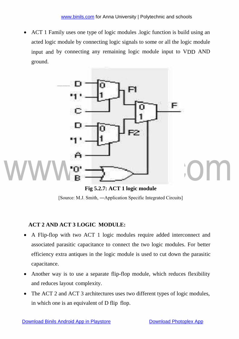
Download Binils Android App in Playstore Download Photoplex App
www.binils.com for Anna University | Polytechnic and schools
ACT 1 Family uses one type of logic modules .logic function is build using an
acted logic module by connecting logic signals to some or all the logic module
input and by connecting any remaining logic module input to VDD AND
ground.
Fig 5.2.7: ACT 1 logic module
[Source: M.J. Smith, ―Application Specific Integrated Circuits]
ACT 2 AND ACT 3 LOGIC MODULE:
A Flip-flop with two ACT 1 logic modules require added interconnect and
associated parasitic capacitance to connect the two logic modules. For better
efficiency extra antiques in the logic module is used to cut down the parasitic
capacitance.
Another way is to use a separate flip-flop module, which reduces flexibility
and reduces layout complexity.
The ACT 2 and ACT 3 architectures uses two different types of logic modules,
in which one is an equivalent of D flip flop.
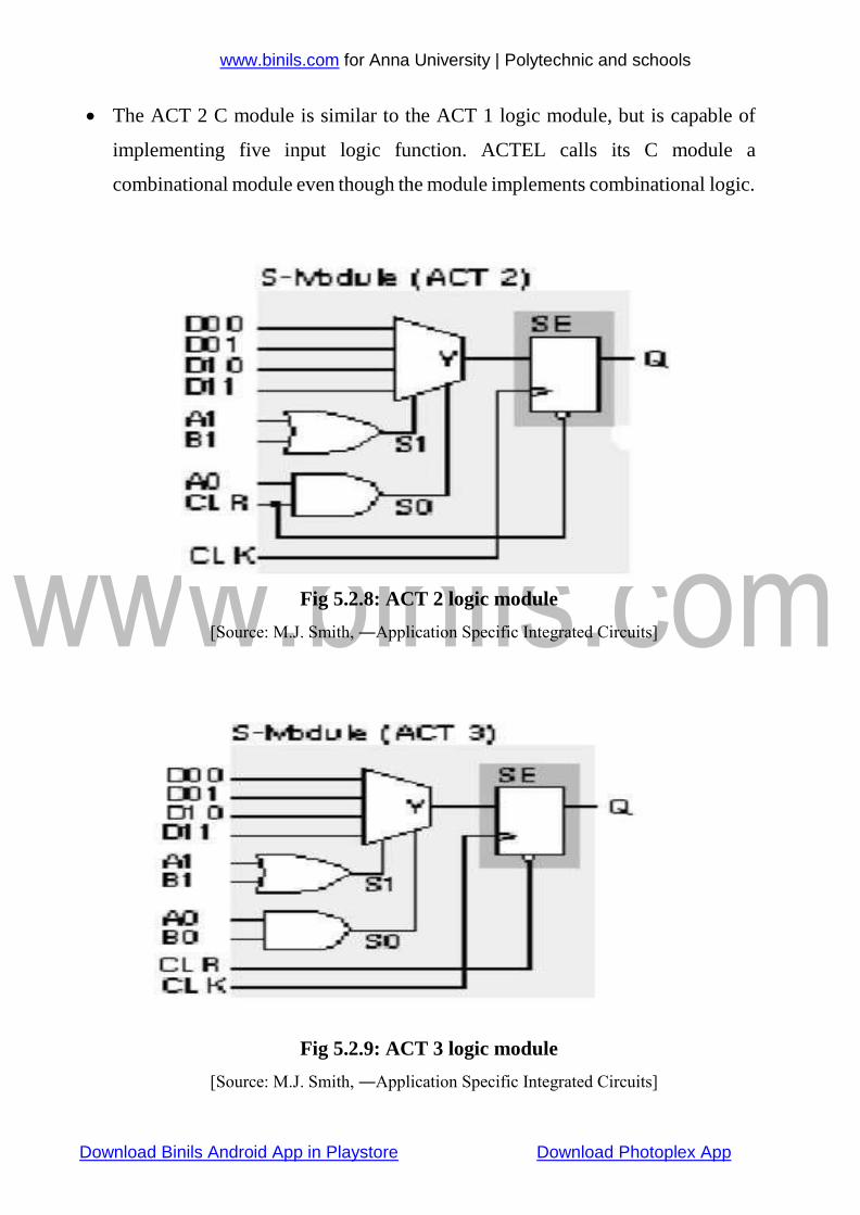
Download Binils Android App in Playstore Download Photoplex App
www.binils.com for Anna University | Polytechnic and schools
The ACT 2 C module is similar to the ACT 1 logic module, but is capable of
implementing five input logic function. ACTEL calls its C module a
combinational module even though the module implements combinational logic.
Fig 5.2.8: ACT 2 logic module
[Source: M.J. Smith, ―Application Specific Integrated Circuits]
Fig 5.2.9: ACT 3 logic module
[Source: M.J. Smith, ―Application Specific Integrated Circuits]
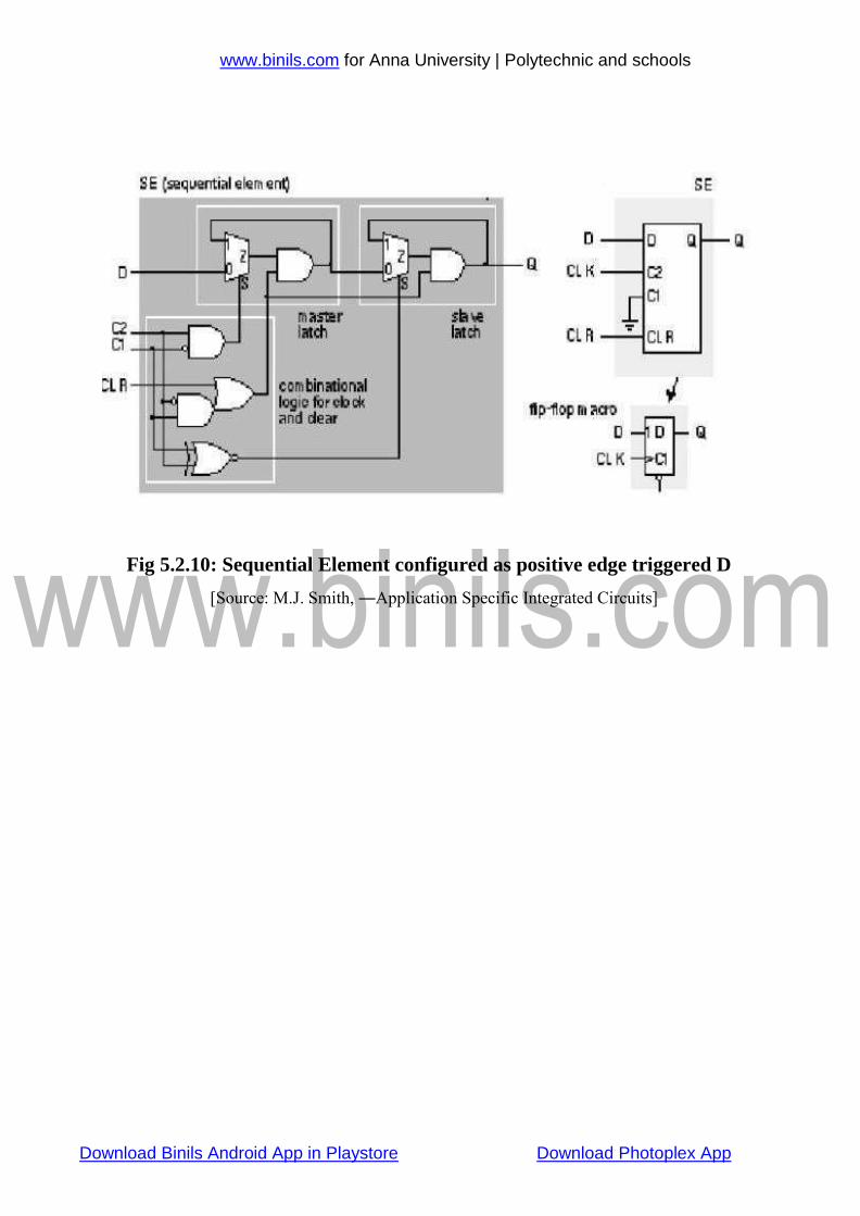
Download Binils Android App in Playstore Download Photoplex App
www.binils.com for Anna University | Polytechnic and schools
Fig 5.2.10: Sequential Element configured as positive edge triggered D
[Source: M.J. Smith, ―Application Specific Integrated Circuits]
www.binils.com for Anna University | Polytechnic and schools
Download Binils Android App in Playstore Download Photoplex App
Scan Design Rules
Only clocked D-type master-slave flip-flops for all state variables should be used.
At least one PI pin must be available for test. It is better if more pins are available.
All clock inputs to flip-flops must be controlled from primary inputs (PIs). There will be no
gated clock. This is necessary for FFs to function as a scan register.
Clocks must not feed data inputs of flip-flops. A violation of this can lead to a race condition
in the normal mode.
Scan Overheads
The use of scan design produces two types of overheads. These are area overhead and
performance overhead. The scan hardware requires extra area and slows down the signals.
IO pin overhead: At least one primary pin necessary for test.
Area overhead: Gate overhead = [4 noff/ (ng+10nff)] x 100%, where ng = number of
combinational gates; off = number of flip-flops; nsff = number of scan flip-flops; For full scan
number of scan flip-flops is equal to the number of original circuit flip-flops. Example: ng =
100k gates, nff = 2k flip-flops, overhead = 6.7%. For more accurate estimation scan wiring
and layout area must be taken into consideration.
Performance overhead: The multiplexer of the scan flip-flop adds two gate-delays in
combinational path. Fan outs of the flip-flops also increased by 1, which can increase the
clock period.
Scan Variations
There have been many variations of scan as listed below, few of these are discussed here.
Mucked Scan
Scan path
Scan-Hold Flip-Flop
www.binils.com for Anna University | Polytechnic and schools
Download Binils Android App in Playstore Download Photoplex App
X
FF
M FF
O SFF
MM
C/L
Serial scan
Level-Sensitive Scan Design (LSSD)
Scan set
Random access scan
MUX Scan
It was invented at Stanford in 1973 by M. Williams & Angell.
In this approach a MUX is inserted in front of each FF to be placed in the scan chain.
Fig. 5.4.1 The Shift-Register Modification approach
[Source: Jacob Baker, Harry W.LI., David E.Boyee, ―CMOS Circuit Design, Layout and Simulation]
Fig. 39.2 shows that when the test mode pin T=0, the circuit is in normal operation mode and
when T=1, it is in test mode (or shift-register mode).
The scan flip-flips (FFs) must be interconnected in a particular way. This approach effectively
turns the sequential testing problem into a combinational one and can be fully tested by
compact ATPG patterns.
There are two types of overheads associated with this method. The hardware overhead due to
three extra pins, multiplexers for all FFs, and extra routing area. The performance overhead
includes multiplexer delay and FF delay due to extra load.
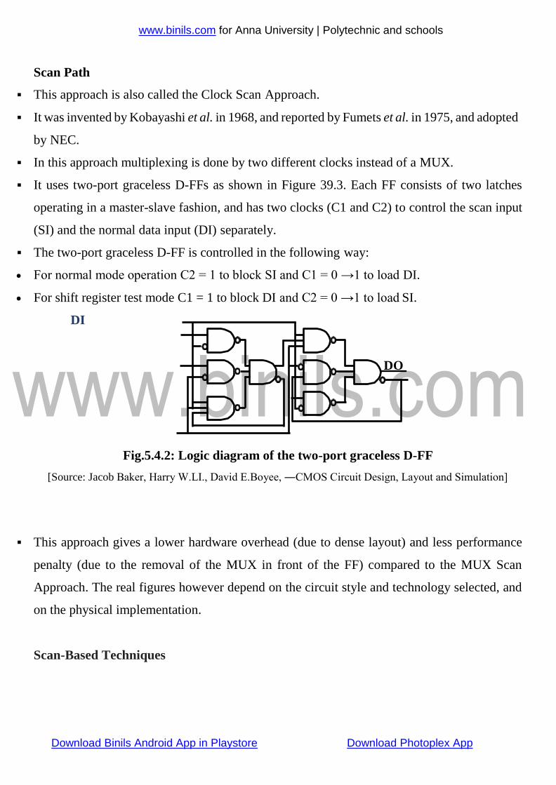
www.binils.com for Anna University | Polytechnic and schools
Download Binils Android App in Playstore Download Photoplex App
Scan Path
This approach is also called the Clock Scan Approach.
It was invented by Kobayashi et al. in 1968, and reported by Fumets et al. in 1975, and adopted
by NEC.
In this approach multiplexing is done by two different clocks instead of a MUX.
It uses two-port graceless D-FFs as shown in Figure 39.3. Each FF consists of two latches
operating in a master-slave fashion, and has two clocks (C1 and C2) to control the scan input
(SI) and the normal data input (DI) separately.
The two-port graceless D-FF is controlled in the following way:
For normal mode operation C2 = 1 to block SI and C1 = 0 →1 to load DI.
For shift register test mode C1 = 1 to block DI and C2 = 0 →1 to load SI.
DI
Fig.5.4.2: Logic diagram of the two-port graceless D-FF
[Source: Jacob Baker, Harry W.LI., David E.Boyee, ―CMOS Circuit Design, Layout and Simulation]
This approach gives a lower hardware overhead (due to dense layout) and less performance
penalty (due to the removal of the MUX in front of the FF) compared to the MUX Scan
Approach. The real figures however depend on the circuit style and technology selected, and
on the physical implementation.
Scan-Based Techniques
DO

www.binils.com for Anna University | Polytechnic and schools
Download Binils Android App in Playstore Download Photoplex App
The controllability and observer ability can be enhanced by providing more accessible
logic nodes with use of additional primary input lines and multiplexors. However, the use of
additional I/O pins can be costly not only for chip fabrication but also for packaging. A popular
alternative is to use scan registers with both shift and parallel load capabilities. The scan design
technique is a structured approach to design sequential circuits for testability.
The storage cells in registers are used as observation points, control points, or both. By
using the scan design techniques, the testing of a sequential circuit is reduced to the problem
of testing a combinational circuit. In general, a sequential circuit consists of a combinational
circuit and some storage elements. In the scan-based design, the storage elements are
connected to form a long serial shift register, the so-called scan path, by using multiplexors
and a mode (test/ normal) control signal, as shown in Fig. 1 .In the test mode, the scan-in signal
is clocked into the scan path, and the output of the last stage latch is scanned out. In the normal
mode, the scan-in path is disabled and the circuit functions as a sequential circuit. The testing
sequence is as follows:
Step 1: Set the mode to test and, let latches accept data from scan-in input. Step
2: Verify the scan path by shifting in and out the test data. Step 3:
Scan in (shift in) the desired state vector into the shift register. Step 4:
Apply the test pattern to the prim ray input pins. Step 5: Set the
mode to normal and observe the primary outputs of the circuit after sufficient time
for propagation. Step 6: Assert
the circuit clock, for one machine cycle to capture the outputs of the combinational logic
into the registers. Step 7: Return to
test mode; scan out the contents of the registers, and at the same time scan in the
next pattern. Step 8: Repeat
steps 3-7 until all test patterns are applied.
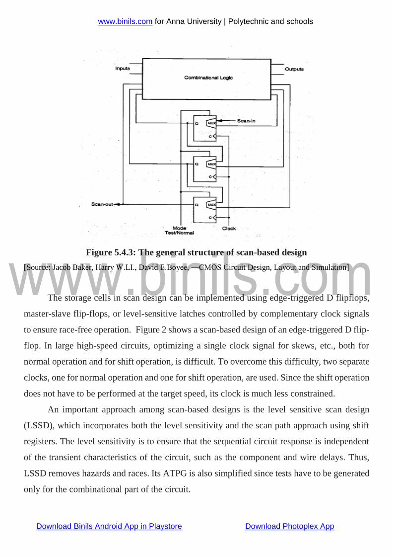
www.binils.com for Anna University | Polytechnic and schools
Download Binils Android App in Playstore Download Photoplex App
Figure 5.4.3: The general structure of scan-based design
[Source: Jacob Baker, Harry W.LI., David E.Boyee, ―CMOS Circuit Design, Layout and Simulation]
The storage cells in scan design can be implemented using edge-triggered D flipflops,
master-slave flip-flops, or level-sensitive latches controlled by complementary clock signals
to ensure race-free operation. Figure 2 shows a scan-based design of an edge-triggered D flip-
flop. In large high-speed circuits, optimizing a single clock signal for skews, etc., both for
normal operation and for shift operation, is difficult. To overcome this difficulty, two separate
clocks, one for normal operation and one for shift operation, are used. Since the shift operation
does not have to be performed at the target speed, its clock is much less constrained.
An important approach among scan-based designs is the level sensitive scan design
(LSSD), which incorporates both the level sensitivity and the scan path approach using shift
registers. The level sensitivity is to ensure that the sequential circuit response is independent
of the transient characteristics of the circuit, such as the component and wire delays. Thus,
LSSD removes hazards and races. Its ATPG is also simplified since tests have to be generated
only for the combinational part of the circuit.
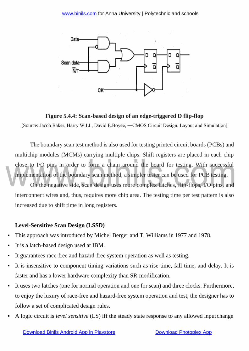
www.binils.com for Anna University | Polytechnic and schools
Download Binils Android App in Playstore Download Photoplex App
Figure 5.4.4: Scan-based design of an edge-triggered D flip-flop
[Source: Jacob Baker, Harry W.LI., David E.Boyee, ―CMOS Circuit Design, Layout and Simulation]
The boundary scan test method is also used for testing printed circuit boards (PCBs) and
multichip modules (MCMs) carrying multiple chips. Shift registers are placed in each chip
close to I/O pins in order to form a chain around the board for testing. With successful
implementation of the boundary scan method, a simpler tester can be used for PCB testing.
On the negative side, scan design uses more complex latches, flip-flops, I/O pins, and
interconnect wires and, thus, requires more chip area. The testing time per test pattern is also
increased due to shift time in long registers.
Level-Sensitive Scan Design (LSSD)
This approach was introduced by Michel Berger and T. Williams in 1977 and 1978.
It is a latch-based design used at IBM.
It guarantees race-free and hazard-free system operation as well as testing.
It is insensitive to component timing variations such as rise time, fall time, and delay. It is
faster and has a lower hardware complexity than SR modification.
It uses two latches (one for normal operation and one for scan) and three clocks. Furthermore,
to enjoy the luxury of race-free and hazard-free system operation and test, the designer has to
follow a set of complicated design rules.
A logic circuit is level sensitive (LS) iff the steady state response to any allowed input change

www.binils.com for Anna University | Polytechnic and schools
Download Binils Android App in Playstore Download Photoplex App
is independent of the delays within the circuit. Also, the response is independent of the order
in which the inputs change
LSSD requires that the circuit be LS, so we need LS memory elements as defined above.
Figure 39.4 shows an LS polarity-hold latch. The correct change of the latch output (L) is not
dependent on the rise/fall time of C, but only on C being `1' for a period of time greater than
or equal to data propagation and stabilization time. Figure 39.5 shows the polarity-hold shift-
register latch (SRL) used in LSSD as the scan cell.
The scan cell is controlled in the following way:
Normal mode: A=B=0, C=0 1.
SR (test) mode: C=0, AB=10 01 to shift SI through L1 and L2.
Advantages of LSSD
1. Correct operation independent of AC characteristics is guaranteed.
2. FSM is reduced to combinational logic as far as testing is concerned.
3. Hazards and races are eliminated, which simplifies test generation and fault simulation.
Drawbacks of LSSD
1. Complex design rules are imposed on designers. There is no freedom to vary from the overall
schemes. It increases the design complexity and hardware costs (4-20% more hardware and 4
extra pins).
2. Asynchronous designs are not allowed in this approach.
3. Sequential routing of latches can introduce irregular structures.
4. Faults changing combinational function to sequential one may cause trouble, e.g., bridging
and CMOS stuck-open faults.
5. Test application becomes a slow process, and normal-speed testing of the entire test sequence
is impossible.
6. It is not good for memory intensive designs.
www.binils.com for Anna University | Polytechnic and schools
Download Binils Android App in Playstore Download Photoplex App
Random Access Scan
This approach was developed by Fujitsu and was used by Fujitsu, Amdahl, and TI.
It uses an address decoder. By using address decoder we can select a particular FF and either
set it to any desired value or read out its value. Random access structure and RAM cell.
The difference between this approach and the previous ones is that the state vector can now be
accessed in a random sequence. Since neighboring patterns can be arranged so that they differ
in only a few bits, and only a few response bits need to be observed, the test application time
can be reduced.
In this approach test length is reduced.
This approach provides the ability to `watch' a node in normal operation mode, which is
impossible with previous scan methods.
This is suitable for delay and embedded memory testing.
The major disadvantage of the approach is high hardware overhead due to address decoder,
gates added to SFF, address register, extra pins and routing
Scan-Hold Flip-Flop
Special type of scan flip-flop with an additional latch designed for low power testing
application.
The control input HOLD keeps the output steady at previous state of flip-flop.
For HOLD = 0, the latch holds its state and for HOLD = 1, the hold latch becomes transparent.
For normal mode operation, TC = HOLD =1 and for scan mode, TC = 1 and Hold = 0.
Hardware overhead increases by about 30% due to extra hardware the hold latch.
This approach reduces power dissipation and isolate asynchronous part during scan.
It is suitable for delay test.
Partial Scan Design
In this approach only a subset of flip-flops is scanned. The main objectives of this approach
www.binils.com for Anna University | Polytechnic and schools
Download Binils Android App in Playstore Download Photoplex App
are to minimize the area overhead and scan sequence length. It would be possible to achieve
required fault coverage
In this approach sequential ATPG is used to generate test patterns. Sequential ATPG has
number of difficulties such as poor initialize ability, poor controllability and observerability of
the state variables etc. Number of gates, number of FFs and sequential depth give little idea
regarding testability and presence of cycles makes testing difficult. Therefore sequential circuit
must be simplified in such a way so that test generation becomes easier.
Removal of selected flip-flops from scan improves performance and allows limited scan
design rule violations.
It also allows automation in scan flip-flop selection and test generation
Design using partial scan architecture [1].
Sequential depth is calculated as the maximum number of FFs encountered from PI line to PO
line.
Things to be followed for a partial scan method
A minimum set of flip-flops must be selected, removal of which would eliminate all cycles.
Break only the long cycles to keep overhead low.
All cycles other than self-lops should be removed.
Related Documents