Peter Kinget (In collaboration with S. Chatterjee and Y. Tsividis) 0.5V Analog Integrated Circuits Department of Electrical Engineering

Welcome message from author
This document is posted to help you gain knowledge. Please leave a comment to let me know what you think about it! Share it to your friends and learn new things together.
Transcript

Peter Kinget
(In collaboration with S. Chatterjee and Y. Tsividis)
0.5V AnalogIntegrated Circuits
Department of Electrical Engineering

www.cisl.columbia.edu
Analog, Digital, Mixed-Mode and RF Integrated Circuits

© Kinget 2005 3
Analog, Mixed Signal and RF Integrated Circuit Design Research
Ultra-low voltage circuits: 0.5V
RF integratedoscillators
Ultra-widebandRF circuits
Injection lockedcircuits
Biological Interfaces
Device mismatch & its influence onAnalog & RF ics

© Kinget 2005 4
Sample of Recent Chips
© Kinget 2005 5
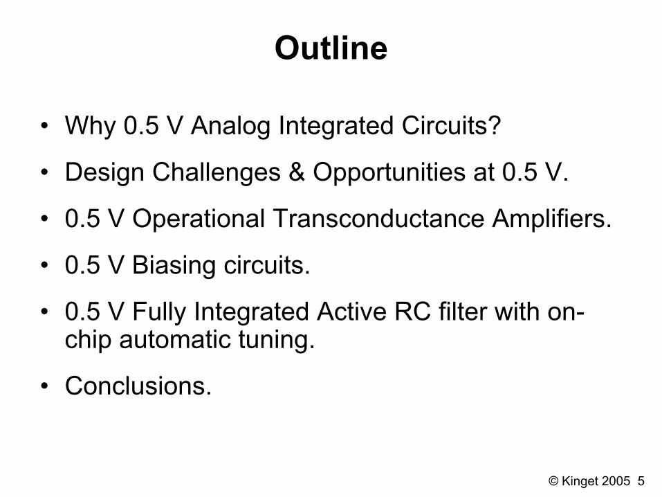
Outline
• Why 0.5 V Analog Integrated Circuits?
• Design Challenges & Opportunities at 0.5 V.
• 0.5 V Operational Transconductance Amplifiers.
• 0.5 V Biasing circuits.
• 0.5 V Fully Integrated Active RC filter with on-chip automatic tuning.
• Conclusions.

© Kinget 2005 6
Analog in a Mixed Signal World• Sounds, images, EM waves, …. are ANALOG.• Information processing & storage are DIGITAL.• System-on-chip is powerful economic paradigm.
• Digital drives technology development & choice.
If Analog can be done in a digital technology, it will be done.
Most Digital ICs need some Analog!
D & A A & D A & D

© Kinget 2005 7
CMOS Trends: Supply Voltage
Analog VDD
Digital VDD
Digital VT
Technology node [nm]
[ITRS'04]
–O– High Perf.–∆– Low Standby–V– Low Power

© Kinget 2005 8
CMOS Trends: On chip Clock Speed
[ITRS'04]
Technology node [nm]

© Kinget 2005 9
MOS transistor
• Transconductor or Current SourceVDS > 0.15V (for VGS-VT ≤ 0.2)
• Switch/Resistoronly for very small signal range !?
SwitchResistor:
TransconductorWeak
Inversion
StrongInversion
0.24µm/0.36µm nMOSin 0.18µm CMOS
5φT

© Kinget 2005 10
Common Source Amplifier
0.15 V
0.15 V
0.2 Vpp
0.5 + 0.15 V
0.5 V
VT= 0.5 V VDS,sat= 0.15 V

© Kinget 2005 11
Common Drain Buffer
0.15 V
0.15 V
0.2 Vpp
0.5 + 0.15 + 0.1 + 0.15 V
0.5 V
VT= 0.5 V VDS,sat= 0.15 V

© Kinget 2005 12
Common Gate Amplifier / Cascode
0.15 V
0.15 V0.5 + 0.15 + x + 0.15 V
0.5 V
VT= 0.5 V VDS,sat= 0.15 V
0.15 V
© Kinget 2005 13
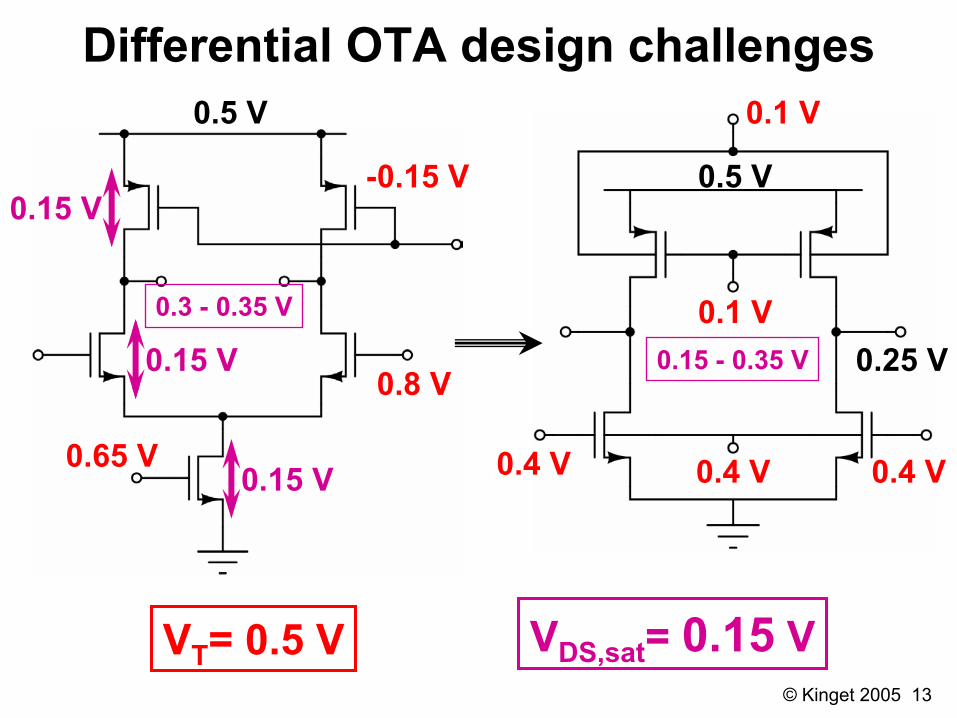
Differential OTA design challenges
0.15 V
0.5 V
0.65 V
0.8 V
-0.15 V
0.15 V
0.15 V
0.3 - 0.35 V
0.5 V
0.1 V
0.4 V0.4 V
0.1 V0.15 - 0.35 V
0.4 V
0.25 V
VT= 0.5 V VDS,sat= 0.15 V

© Kinget 2005 14
CMFB in Folded Cascode OTA
Common Mode Feedback requires ‘fast’ amplifier operating from Vout,CM= VDD/2 !?

© Kinget 2005 15
Challenges at 0.5 V• VDS,sat related challenges:
– Independent of region of operation!– Independent of VT!– Signal swings are limited.– Avoid transistor stacks.
• VGS related challenges:– Depend on region of operation & (VGS-VT).– Depend on VT!– Avoid signal swing on gate.

© Kinget/Chatterjee/Tsividis 16
‘Feedback to the rescue’
CM @ OTA-in > CM @ input and output
[Kar00] [Bul00]

© Kinget/Chatterjee/Tsividis 17
Opportunities at 0.5 V: MOS 4-terminal device
Body
Source
Drain
Gate
G D BS Sub
n+
n+n+n+ n+p+ p+
p
p
nMOS cross section(deep n-well process)
nMOS circuit equivalent(deep n-well process)

© Kinget/Chatterjee/Tsividis 18
Opportunities at 0.5 V• Body terminal
– Signal input: [Guz87]– VTH reduction & control
[Kob94], [Von94]– Bias control
• Latch-up not an issue– Assuming VDD and GND are
‘well behaved’.• Techniques can be ported
to ‘double gate’ devices
VBS 0.5 V
500
0
VTH
mV
300
430360
0.0
VGS 0.5 V0.2
3
0
IDS VBS ↑
µA
0.24µm/0.36µm nMOSin 0.18µm CMOS

0.5 V Body-input OTA

© Kinget/Chatterjee/Tsividis 20
Low-voltage differential-gain stage
0.15 - 0.35 V
0.5 V0.25 V
0.25 V
0.25 V
0.07 V

© Kinget/Chatterjee/Tsividis 21
Single-stage gain, CMRR
Differential mode load: gds
Common mode load: (gm1 + gm3)

© Kinget/Chatterjee/Tsividis 22
Two-stage fully-differential OTA
Pole splitting using Miller capacitor

© Kinget/Chatterjee/Tsividis 23
Setup for open-loop measurements
0.18 µm CMOS

© Kinget/Chatterjee/Tsividis 24
Open loop frequency response
DC gain: 52 dBGBW: 2.5 MHz
Phase Margin: 450
Frequency [Hz]
Simulation
Measurement

© Kinget/Chatterjee/Tsividis 25
Bulk-input OTA performanceC
lose
d lo
opO
pen
loop

0.5 V Gate-input OTA
© Kinget/Chatterjee/Tsividis 27
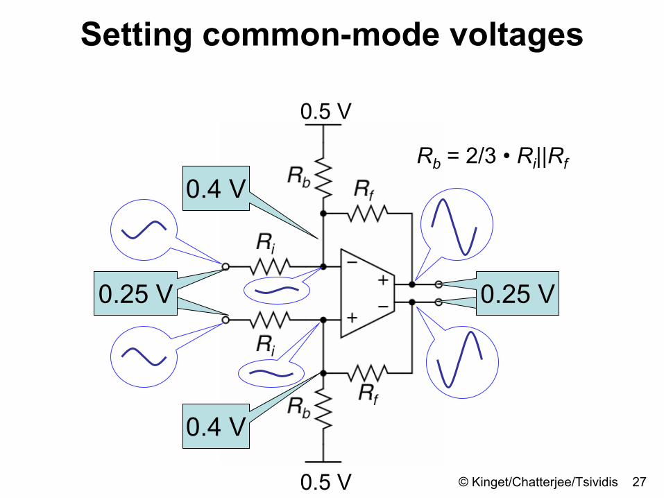
Setting common-mode voltages
0.5 V
0.4 V
0.4 V
0.5 V
Rb = 2/3 • Ri||Rf
0.25 V 0.25 V

© Kinget/Chatterjee/Tsividis 28
0.5 V OTA gate-input stage

© Kinget/Chatterjee/Tsividis 29
Two stage OTA
• Common-mode output of first stage is 0.4 V
0.25 V
0.4 V
0.4 V
© Kinget/Chatterjee/Tsividis 30
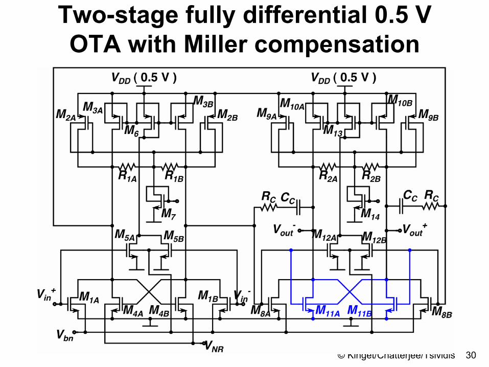
Two-stage fully differential 0.5 V OTA with Miller compensation

© Kinget/Chatterjee/Tsividis 31
Open Loop Performance (meas.)
Frequency [Hz]
Gai
n [d
B]
42 dB
GBW: 10 MHz
CL= 10pF (diff.)RL= 50kΩIDD= 150 µA
62 dB 350mV; automatic bias

© Kinget/Chatterjee/Tsividis 32
66.711.413289.5100 η [1/V]
----Depl.MOS
Lat.BJT
-Lat.BJT
SpecialDevices
0.180.180.50.72.50.50.352Techn. [um]
DDDSSSSSSE/Diff.101014-1220722CL [pF]75110-4600.5-5300Power [uW]102.541.36e-31.30.21.3GBW [MHz]
50/6252598470537049ADC [dB]0.50.50.91.30.90.811VDD [V]
G-IB-I[Pel98]
[Fer96]
[Sto02]
[Leh01]
[Las00]
[Bla98]
On-chip automatic biasing circuits

© Kinget/Chatterjee/Tsividis 34
On-chip biasing circuits
Vbn generating circuit
Level shift biasing circuit
(Simplified OTA)

© Kinget/Chatterjee/Tsividis 35
Error amplifier for biasing
• 20 kHz GBW for 1 pF load• 2 µA current• Controlled body voltage sets the amplifier threshold
Vin Vout
Vou
t[V
]
Vin [V]

© Kinget/Chatterjee/Tsividis 36
OTA dc transfer characteristics and VNR generation
VNR generating circuit
Replica of OTA stage 1
Input differential voltage [mV]
Out
put d
i ff v
olta
g e [V
]
Increasing VNR

© Kinget/Chatterjee/Tsividis 37
Open Loop Performance (meas.)
Frequency [Hz]
Gai
n [d
B]
42 dB
GBW: 10 MHz
CL= 10pF (diff.)RL= 50kΩIDD= 150 µA
62 dB 350mV; automatic bias

0.5 V Continuous time tunable active RC Filter
© Kinget/Chatterjee/Tsividis 39
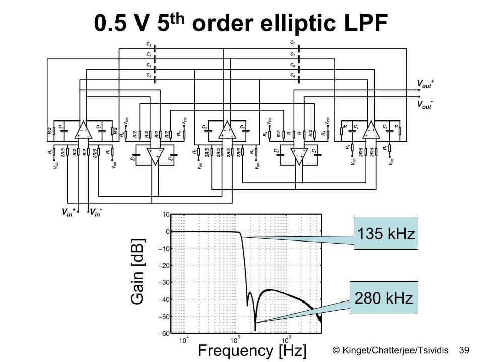
0.5 V 5th order elliptic LPF
Frequency [Hz]
Gai
n [d
B]
280 kHz
135 kHz

© Kinget/Chatterjee/Tsividis 40
Filter tuning challenges at 0.5 V• Gm-C• MOSFET-C• Switching banks of R’s and C’s• Varactor-R techniques
Vtune [V]
Cgs
/Cox
Gate (0.4 V) Source
Drain (0.25 V)
Body (Vtune)

© Kinget/Chatterjee/Tsividis 41
Low-voltage tunable integrator
0.25 V 0.25 V
0.4 V
+
-Vin Vout
+
-
VDD
VDD

© Kinget/Chatterjee/Tsividis 42
Die photograph
• 0.18 µm CMOS
• MIM capacitors
• High-res resistors
• Standard VT
• Triple well devices
Filter PLL
Biasing circuits
OTAs
1mm
1mm

© Kinget/Chatterjee/Tsividis 43Frequency [Hz]
Gai
n [d
B]
Measured filter response for different supply voltages

© Kinget/Chatterjee/Tsividis 44
Measured filter response for different tuning voltages
Frequency [Hz]
Gai
n [d
B]
88 - 154 kHz(1.75x)

© Kinget/Chatterjee/Tsividis 45
Measured filter response for different chips
Frequency [Hz]
Gai
n [d
B]
1.3 % std dev in cut-off
frequency for 20 samples

© Kinget/Chatterjee/Tsividis 46
Measured 3rd order inter-modulation
25 kHz
20 kHz
15 kHz
30 kHz
40 dB
Input differential rms amplitude [V]
Out
put d
iffe r
entia
l rm
s am
plitu
d e [ V
]

Effect of gain enhancement
Frequency [Hz]
Gai
n [d
B]
Without gain-enhancement
With gain-enhancement

© Kinget/Chatterjee/Tsividis 48
Performance summary at 27C
727285104VCO feed-thru @280kHz [µV rms]
69.0150.5
84.5148.0
88.0154.5
96.5153.0
Tuning range [kHz] Vtune = VDD
Vtune = 0.0 V
58575755Dynamic range [dB]5353Out-of-band IIP3 [dBV]-3-3-3-5In-band IIP3 [dBV]50505050Input [mV rms] (100kHz / 1% THD)65687487Noise [µV rms]4.33.32.21.5Total current [mA]
135.0135.0135.0135.0-3 dB cut-off frequency [kHz]0.600.550.500.45VDD [V]
Functionality tested from 5C to 85C at 0.5 V
• Measured CMRR (10 kHz common mode tone): 65 dB• Measured PSRR (10 kHz tone on power supply): 43 dB

© Kinget/Chatterjee/Tsividis 49
Conclusions• Developed true low voltage design
techniques for 0.5 V analog circuits.• Low voltage OTAs designed - can be used as
building block in other designs.• Automatic biasing and tuning through bodies
of devices.• PLL-tuned 5th order elliptic low-pass filter
demonstrated.• Step towards 0.5 V analog circuits for the
nano-scale CMOS era

© Kinget 2005 52
Acknowledgments
• Analog Devices for supporting part of this work.

© Kinget 2005 53
More details
• [Cha 05] S. Chatterjee, Y. Tsividis, and P. Kinget, "A 0.5 V filter with PLL-based tuning in 0.18 um CMOS technology," in IEEE International Solid-State Circuits Conference (ISSCC), pp. 506-507, February 2005.
• [Cha 04] S. Chatterjee, Y. Tsividis, and P. Kinget, "A 0.5 V bulk input fully differential operational transconductance amplifier," in European Solid-State Circuits Conference (ESSCIRC), pp.147-150, September 2004.

© Kinget 2005 54
References• [Guz 87] A. Guzinski, M. Bialko, and J. Matheau, "Body driven
differential amplifier for application in continuous-time active-C filter,''Proceedings of ECCD, pp. 315--319, 1987.
• [Bla 98] B. Blalock, P. Allen, and G. Rincon-Mora, "Designing 1-V op-amps using standard digital CMOS technology,'‘ IEEE Trans. Circuits Syst. II, vol. 45, pp. 769--780, July 1998.
• [Las 00] K. Lasanen, E. Raisanen-Ruotsalainen, and J. Kostamovaara, "A 1-V 5 µW CMOS-opamp with bulk-driven input transistors,'' 43rd IEEE Midwest Symposium on Circuits and Systems, pp. 1038--1041, 2000.
• [Leh 01] T. Lehmann and M. Cassia, "1-V power supply CMOS cascode amplifier,'' IEEE J. Solid-State Circuits, vol. 36, pp. 1082--1086, July 2001.
• [Sto 02] T. Stockstad and H. Yoshizawa, "A 0.9-V 0.5-µA rail-to-rail CMOS operational amplifier,'' IEEE J. Solid-State Circuits, vol. 37, no. 3, pp. 286--292, 2002.
• [Fer 96] G. Ferri and W. Sansen, "A 1.3V opamp in standard 0.7µmCMOS with constant gm and rail-to-rail input and output stages,''IEEE International Solid State Circuits Conference, pp. 382--383, 478, 1996.

© Kinget 2005 55
References• [Pel 98] V. Peluso, P. Vancorenland, A. M. Marques, M. Steyaert,
and W. Sansen, "A 900-mV low-power ∆Σ A/D converter with 77-dB dynamic range,'' IEEE J. Solid-State Circuits, vol. 33, no. 12, pp. 1887--1897, Dec. 1998.
• [Kob94] T. Kobayashi and T. Sakurai, “Self-adjusting threshold-voltage scheme (SATS) for low-voltage high-speed operation,” in IEEE Custom Integrated Circuits Conference (CICC), May 1994, pp. 271–274.
• [Von94] V. R. Kaenel, M. D. Pardoen, E. Dijkstra, and E. A. Vittoz, “Automatic adjustment of threshold and supply voltages for minimum power consumption in CMOS digital circuits,” in IEEE Symposium on Low Power Electronics, pp. 78–79, 1994.
• [Kar00] S. Karthikeyan, S. Mortezapour, A. Tammineedi, and E. Lee, “Low-voltage analog circuit design based on biased inverting opampconfiguration,” IEEE Trans. Circuits Syst. II, vol. 47, no. 3, pp. 176–184, March 2000.
• [Bul00] K. Bult, “Analog design in deep sub-micron CMOS,” in European Solid-State Circuits Conference (ESSCIRC),September 2000, pp. 11–17.
Related Documents