UNIVERSITY OF CALIFORNIA, IRVINE
Thermoelectric Behavior in Lead Selenide Nanocrystal Films
THESIS
Submitted in partial satisfaction of the requirements for the degree of
MASTER OF SCIENCE
in Materials Science and Engineering
by
Alvin Ly
Thesis Committee: Assistant Professor Allon Hochbaum, Chair
Professor Matthew Law Professor Julie Schoenung
2018

© 2018 Alvin Ly

ii
TABLE OF CONTENTS
Page LIST OF FIGURES...........................................................................................................iii ACKNOWLEDGMENTS..................................................................................................vii ABSTRACT....................................................................................................................viii 1. Introduction..................................................................................................................1
1.1 History of thermoelectrics......................................................................................1 1.2 Basic thermoelectricity concepts...........................................................................5 1.3 Thermoelectric device applications.......................................................................8 1.4 Thermoelectric Materials.....................................................................................11
1.3.1 Bulk Materials.............................................................................................12 1.3.2 Nanostructured Materials............................................................................14
2. Methodology..............................................................................................................21 2.1 Chemicals............................................................................................................21 2.2 Nanocrystal synthesis.........................................................................................21 2.3 Device fabrication................................................................................................22 2.3.1 Film deposition............................................................................................22 2.3.2 Hydrogen Sulfide Treatment and Atomic Layer Deposition........................24 2.4 Device characterization.......................................................................................25
3. Results and Discussion.............................................................................................28 3.1 Nanocrystal and ligand analysis..........................................................................28 3.2 Film structural analysis and stability....................................................................32 3.3 Electrical behavior...............................................................................................34 3.4 Thermoelectric behavior......................................................................................36
4. Conclusion.................................................................................................................43 5. Future Works.............................................................................................................45 6. References................................................................................................................47

iii
LIST OF FIGURES Figure 1.1 Thomas Seebeck and the instrument he used to observe a compass needle deflecting due to a current induced through the heating of one junction of two different metals. Figure 1.2 Gustav Magnus and the voltage difference, V, induced across the terminals of an open circuit between two different metals. The junctions of A and B, representing the two metals, held at different temperatures is directly proportional to the difference in temperature of the two sites. Figure 1.3 USA space missions that used a radioisotope thermoelectric generator as the electrical power source and the anatomy of a radioisotope thermoelectric generator that was used in the Voyager 1 and Voyager 2 space missions. Figure 1.4 Power generation efficiency equation. Figure 1.5 Thermoelectric figure of merit equation Figure 1.6 Dependence of ZT and power factor on Seebeck coefficient, electrical conductivity, thermal conductivity, and carrier concentration. Figure 1.7 Diagram showing the transport of phonons and electrons in a thermal gradient with defect and grain boundary scattering. Figure 1.8 Anatomy of a typical thermocouple temperature sensing probe. Figure 1.9 Schematics of thermoelectric modules for power generation, where a temperature gradient creates charge carrier movement inducing current flow with a complete circuit, and active refrigeration, where an applied current creates charge carrier movement inducing a temperature gradient across the material. Figure 1.10 Typical ZT values of common thermoelectric materials with respect to temperature. Figure 1.11 Schematic and diagram of the Czochralski single crystal growth method.

iv
Figure 1.12 Geometry of a two legged thermoelectric cooling device and scanning electron microscopy image of superlattice thin film. Figure 1.13 Thermoelectric maximum temperature differentials from room temperature of a standard two-leg thermoelectric cooling device made from current lead salt superlattice materials, commercial bulk solid solution alloyed materials, current one-leg superlattice device with parasitic losses, current one-leg bulk materials with parasitic losses. Figure 1.14 Scanning electron microscopy image of a single nanowire thermoelectric device and image of a nanowire array thermoelectric device. Both devices have resistive heating coils on opposite ends of the devices. Figure 1.15 Quantum dots, or colloidal nanocrystals, showing different photoluminescence colors depending on nanocrystal size and the splitting of energy levels in quantum dots due to confinement effects compared to bulk materials. Figure 2.1 Typical three-neck flask nanocrystal synthesis procedure with cadmium selenide precursors shown. Figure 2.2 Substrate patterns of double-side polished silicon, field effect transistor (FET), thermoelectric devices. Small scratches in the corner of the FET and thermoelectric substrates indicate where the oxide was typically scratched away to contact the back-gate. Figure 3.1 One-pot lead selenide nanocrystal synthesis set-up. Figure 3.2 Optical absorption spectrum of lead selenide nanocrystals showing red shift after ligand exchange Figure 3.3 Optical absorption spectrum of two separate synthesis batches absorbing around the target wavelength of 1800 nm. Figure 3.4 Fourier transform infrared spectroscopy (FTIR) spectra showing signature C-H stretching and carbonyl stretching of the oleate ligands.

v
Figure 3.5 Full FTIR spectra of oleate capped films and full exchanged 1,2-ethandithiol (EDT) capped nanocrystal films. Figure 3.6 Zoomed FTIR spectra of C-H stretching and COO- stretching in oleate capped and fully exchanged EDT capped nanocrystal films. Figure 3.7 Top down images at different magnifications of lead selenide nanocrystal films treated with 1,2-ethanedithiol showing crack-free, even distribution of nanocrystals with no long range ordering. Figure 3.8 Cross sectional view of field effect transistor and thermoelectric substrates showing the flat layers of lead selenide nanocrystals and alumina overcoating. Figure 3.9 Bias-stress effect showing transient behavior on linear and log scales with pre-ALD and post-ALD data. Figure 3.10 Pre-ALD field effect transistor behavior of lead selenide nanocrystal film devices. Figure 3.11 Post-ALD field effect transistor behavior of lead selenide nanocrystal film devices. Figure 3.12 Schematic and picture of the home built thermopower measurement system. Figure 3.13 Diagram of a temperature measurement set-up and equation to calculate the temperature from the resistance of our contact metal. Figure 3.14 Seebeck coefficient graphs of silicon standard samples and compiled table of dopant type, resistivities, and Seebeck coefficients of the standards. Figure 3.15 Example graphs of raw data plots for pre-ALD and post-ALD lead selenide nanocrystal film thermoelectric devices. Figure 3.16 Example graphs of calculated Seebeck coefficient and temperature different values of two pre-ALD lead selenide nanocrystal film thermoelectric devices.

vi
Figure 3.17 Example graphs of calculated Seebeck coefficient and temperature different values of two pre-ALD lead selenide nanocrystal film thermoelectric devices.

vii
ACKNOWLEDGEMENTS
First and foremost, I would like to offer my gratitude to my advisor, Professor Allon Hochbaum, for the opportunity to learn and grow under his guidance. Upon completion of a few of his courses, I knew that I could benefit immensely from working under him. I was thoroughly impressed by the amount of care and effort that he put into making sure that all of his students succeeded. I am very thankful for the opportunity to work under Prof. Hochbaum. I must also extend my gratitude to Professor Matthew Law, who allowed for this project to fully develop. Professor Law happily invited me to share his laboratory space in order to carry out this project to its potential. I am also extremely grateful of his offer in opening his doors for private and group meetings for me. During my studies here, students and colleagues were often my first source of advice. Mr. Benjamin Adam Wells, an undergraduate student in the Law Lab and my partner on the thermoelectric project, has helped immensely with the development of the project. Mr. Wells should be credited with designing the thermoelectric electric measurement station as well as implementing the code required for thermoelectric properties analysis. Without Mr. Wells, this project would have never made it as far as it did as quickly as it did. I would also like to extend my appreciation all of the members of the Hochbaum Lab and the Law Lab in accepting me as part of their group and aiding me in times of need. I would also like to thank all of the students, staff, and faculty of the Chemical Engineering and Materials Science department at University of California, Irvine for creating an incredible academic experience during my time here as a student. Lastly, I would like to thank my family who has been so supportive of me, financially and emotionally through all of my studies. I hope that my accomplishments and future works will make them proud.

viii
ABSTRACT
THERMOELECTRIC BEHAVIOR IN LEAD SELENIDE NANOCRYSTAL FILMS
By
Alvin Ly
University of California, Irvine, 2018
Master of Science, Materials Science and Engineering
Professor Allon I. Hochbaum, Chair
Thermoelectric power generation could be crucial in a sustainable energy future through
waste heat energy recycling. Typical nanoengineering of thermoelectric materials
requires energy intensive and expensive methods of device fabrication. We employ a
facile solution processed device fabrication method that can easily be scaled up for
manufacturing while maintaining its cost effectiveness. In this work, we establish and
qualify a thermopower measurement system for thin film and bulk devices. To qualify
the measurement system, we show that trends in the signs and magnitudes of the
Seebeck coefficients of known silicon standards are correct. We also show that PbSe
nanocrystal thin film devices exhibit a large Seebeck coefficient (~1500-2000 µV/K)
prior to alumina infilling and a reduced Seebeck coefficient (~800-1200 µV/K) post
alumina infilling. With this measurement tool, we are able to view differences in
thermopower before and after atomic layer deposition treatment within an oxygen-free
atmosphere.

1
1. Introduction
The rising demand for energy along with the degradation of the environment has
pushed research to look into more efficient alternative and “green” energies. Much of
the world’s energy is lost as heat and many thermoelectric materials are being
developed to harvest some of the wasted heat[1,2]. Waste heat is an essentially “free”
energy source for thermoelectric generators. However, thermoelectric devices have
typically been plagued by low efficiencies that outweigh the costs to manufacture such
devices[1]. Converting the world’s waste heat energy into electrical energy could
potentially play an important role in reducing greenhouse gases and conserving
nonrenewable energy sources. Thermoelectric devices could also be used in large-
scale solid-state refrigeration, small-scale electronics cooling, maintenance-free power
generation, and “power-less” implantable medical devices. Although thermoelectric
power generators will most likely not surpass conventional methods in efficiency and
output, these devices could still mitigate a large portion of our energy crisis from
recycling waste into power[1].
1.1 History of thermoelectrics
Thermoelectricity was originally discovered in the late 1700s, independently
rediscovered in the early 1800, but most famously credited to physicist Thomas Johann
Seebeck[3]. The Seebeck effect is the conversion of heat into electricity and was found
through the observation that a compass needle could be deflected by a closed loop or
circuit formed using two different metals with junctions at different temperatures[4]. The
Peltier effect was also discovered in the early 1800s and explains the cooling or heating
at the junction of two different conductors by the direction current flows through the

2
junctions. A supplemental effect named the Thomson effect was found that a
proportional heat is either absorbed or produced when current flows in a material with a
temperature gradient and that proportion depended on the magnitude of the electric
current and temperature gradient[5]. The Seebeck effect is commonly associated with
thermoelectric power generation whereas the Peltier effect is commonly associated with
thermoelectric cooling and refrigeration.
It was found later that the voltage induced in the metals through heating of a
junction was proportional to the temperature difference between the junctions. A
constant coefficient, often known as the Seebeck coefficient or thermopower, was
created to describe this potential. Another important finding during this time was that the
Seebeck voltage did not depend on any temperature distribution across the materials
but rather it was a thermodynamic state function[4]. This allowed for the development of
thermocouples, which are thermoelectric generators that produce dynamic voltages
Figure 1.1 Thomas Seebeck and the instrument he used to observe a compass needle deflecting due to a current induced through the heating of one junction of two different metals.[6]

3
depending on the temperature surrounding the materials that can be used to back-
calculate the temperature.
In the early 1900s, a relationship describing the efficiency of a thermoelectric
cooler or generator was developed and later named the “Figure of Merit” or ZT[7,10]. It
was found that good thermoelectric materials should have large Seebeck coefficients
with high electrical conductivity, to minimize Joule heating from resistance, and low
thermal conductivity, to stabilize a large temperature gradient. The typical material that
best fits these parameters was found to be heavily doped semiconductors, especially
antimony telluride, bismuth telluride, and lead telluride. H. Julian Goldsmid, a leader in
the push for thermoelectricity, was one of the first to realize that having a high mobility
and effective mass combination with low lattice thermal conductivity in properly doped
semiconductors made very good thermoelectric materials[8,11]. A general strategy for
discovering new materials to characterize for thermoelectric properties is choosing a
heavy element and small band gap semiconductor. In the field of thermoelectrics, the
Figure 1.2 Gustav Magnus. The voltage difference, V, induced across the terminals of an open circuit between two different metals. The junctions of A and B ,representing the two metals, held at different temperatures is directly proportional to the difference in temperature of the two sites.[6]

4
term often passed around for the ideal material is a “phonon-glass electron-crystal” type
due to phonons being disrupted the best in a glass and electrons having the best
mobility in crystalline materials[12].
During the mid 1900s, research in thermoelectricity especially in power
generation applications flourished and many thought that this technology would replace
conventional heat engines someday[8]. Progress boomed in the beginning and generator
efficiencies were able to reach ~5% and freezing temperature coolers were developed.
However, progress soon tapered and scientists believed that the upper limit of ZT might
exist around 1.
Although thermoelectric devices weren’t able to reach efficiencies of conventional
processes, the solid-state character of thermoelectric devices allowed it to be useful in
niche applications. Such applications include thermocouples (to take accurate
temperature readings), Peltier coolers (for optoelectronics, mini-refrigeration, and seat
heating/cooling), and radioisotope thermoelectric power generation in space electronics
(by using the radioactive decay heat of a source to generate electricity)[13]. In the last
decade or two, there has been a newfound push to optimize current and develop new
classes thermoelectric materials and devices[14]. Nanoscale engineering has revitalized
research in thermoelectricity and there is hope that engineering structures could
improve ZT for devices to reach conventional process efficiencies[15].

5
1.2 Basic thermoelectricity concepts
Generally, the efficiency of thermoelectric materials relies on a built up
temperature gradient across the material (ΔT) and its ability to efficiently produce
thermoelectric power (ZT). Power generation efficiency (η) is usually defined by the
amount of energy provided to the load over the amount of heat energy absorbed at the
hot junction and is quantitatively shown by combining the Carnot efficiency (ΔT/Thot) and
the dimensionless figure of merit (ZT) shown in the following equation 1.4.
η = !!!!!!!
!!!"!!
!!!"!!!!!
Th and Tc represent the temperatures of hot and cold sides in the thermoelectric device.
The ZT used in the equation takes into account the average temperature of the
gradient. The efficiency equation shows that materials with a large ZT value and the
ability to sustain a large temperature gradient will have the highest efficiencies.
(1.4)
Figure 1.3 USA space missions that used a radioisotope thermoelectric generator as the electrical power source. The anatomy of a radioisotope thermoelectric generator that was used in the Voyager 1 and Voyager 2 space missions.[6]

6
Currently, thermoelectric devices are mostly limited to ZT of ~1 with few materials
showing ZT values of ~2-4 and operate at efficiencies of about 5%.[15] If we are able to
increase ZT by a factor of 4, the projected efficiency may increase to ~25-30%.[15]
ZT, a dimensionless figure of merit, represents the ability of a given material to
efficiently produce thermoelectric power. It is defined by the following equation 1.5.
𝑍𝑇 = !!!"!
T represents the average temperature of the gradient, σ represents the electrical
conductivity, κ represents the thermal conductivity, and S represents the Seebeck
coefficient (a measure of the magnitude of induced voltage in response to a
temperature difference across the material). To obtain the best ZT values, we must
increase the Seebeck coefficient and electrical conductivity while decreasing the
thermal conductivity. This seems like a simple task, however these parameters are
determined by the material’s electronic structure and charge carrier (holes or electrons)
scattering and are not independent of each other. Note that the quantity S2σ is typically
known as the “power factor” and is key to achieving a high performing device. Materials
with a higher power factor value are able to extract more energy out of the temperature
difference, however a high power factor does not necessarily mean that the material is
more efficient at generating this energy.
(1.5)

7
For the best efficiency, materials with high electrical conductivity, low thermal
conductivity, and large Seebeck coefficient are preferred. The best thermoelectric
materials are usually found to be highly doped semiconductors. This is due to the
unique band structure and conductivities of semiconductor materials. Electrical
conductivity of insulating materials is too small to make an impact, even though the
thermal conductivity could be very low and although electrical conductivity of metals is
very high, the thermal conductivity is also very high. Thermal conductivity can be broken
down into two general portions, a contribution from the majority carrier, usually
electrons, and a contribution from phonons. From the Wiedemann-Franz law, we know
that the electron contribution to total thermal conductivity increases as electrical
conductivity increases. As a result, metals typically have a fixed ratio of thermal to
electrical conductivity due to electron domination as a charge carrier, but
semiconductors have a significant phonon contribution, which cannot be neglected. This
phonon contribution will reduce the efficiency, so a low ratio of phonon to electron
Figure 1.6 Dependence of ZT and Power Factor on Seebeck coefficient, electrical conductivity, thermal conductivity, and carrier concentration.[14]

8
contribution is preferred. Highly doped semiconductors are useful in order to reduce the
phonon contribution and keep electrical conductivity high.
The famous phrase “phonon-glass, electron-crystal” stems from the previous
thought. Phonons, responsible for thermal conductivity, should experience the material
as a glass with high degrees of scattering, thus lowering thermal conductivity. Electrons,
usually the primary charge carrier, should experience the material as a crystal with little
scattering, thus maintaining a high conductivity. Most of the work in the recent years has
been focused on attempting to tune these properties independently.
1.3 Thermoelectric Device Applications
Thermoelectric applications are broken down into three main categories: (1)
temperature measurement instruments, (2) thermoelectric cooling, and (3)
thermoelectric power generation.
Figure 1.7 Diagram showing the transport of phonons and electrons in a thermal gradient with defect and grain boundary scattering.[17]

9
Thermocouples are devices that use the Seebeck effect in order to measure a
temperature difference between two different materials. The standard configuration for
thermocouples is shown in figure. The ends of two dissimilar conductors are placed
together to form a probe, which senses the temperature of the environment it is placed
in. The two exposed ends of the two conductors are then connected to a circuit with a
voltmeter, which measures the voltage produced between the two conductors and
translates that voltage measurement into a temperature output through a quick
calculation with the known Seebeck coefficient. An advanced setup of thermocouples
electrically connected in series is known as a thermopile and can be used for high
sensitivity measurements of very small temperature differences.
Thermoelectric cooling is useful in manufacturing refrigerators that are compact
and have no circulating fluid/gas or moving parts. Thermoelectric refrigerators take
advantage of the Peltier effect in which two conductors are put together to form two
junctions and when a current is made to flow through the junctions then one end will be
cooled and one end will be heated. Peltier coolers have poor efficiency and high cost,
however in niche applications the coolers serve as important components that have a
long lifetime and are relatively invulnerable.[29] The cooling effect is the main effect that
is being developed, however there are also applications in which the heating effect is
Figure 1.8 Anatomy of a typical thermocouple temperature sensing probe.

10
used, such as some car seat warmers.[6] Most thermoelectric cooling applications have
not been able to manufactured into consumer products, but they have a wide variety of
use in science. A few of the applications include thermal cyclers used for polymerase
chain reaction (PCR) require rapid heating and cooling of the reaction mixture, stable
temperature controllers that require high precision temperature settings, and modified
computer component heat sink technology to allow for stable functioning when
overclocking.[30]
Thermoelectric power generation is the most widely researched topic within
thermoelectric materials due to its impact on society if successful. Historically,
thermoelectric generators had been researched in order to replace heat engines, which
are bulky and have moving parts, however thermoelectric generators are typically more
Figure 1.9 Schematics of thermoelectric modules for power generation (left), where a temperature gradient creates charge carrier movement inducing current flow with a complete circuit, and active refrigeration (right), where an applied current creates charge carrier movement inducing a temperature gradient across the material.[28]

11
expensive and less efficient. The more recent research thrusts have been to develop a
waste heat conversion thermoelectric generator in order to capture most of the waste
energy in our world that escapes as heat.[31,32,33] Since waste heat is an essentially free
source of input energy, thermoelectric generators can have very low efficiencies as long
as the cost of the material doesn’t outweigh the amount of energy converted. Waste
heat generator applications could be especially useful in power plants and automobiles
as it was found that approximately 75% of the energy produced during combustion is
lost in the exhaust or engine coolant in the form of heat.[6,33] A similar application is a
radioisotope thermoelectric generator, which feeds off a radioisotope as the heat source
for the temperature gradient and is used mainly in space exploration related
technologies due to its longevity and reliability.[6] Cogeneration power plants and
applications have also recently come into light, where the heat produced during
electricity generation is also redirected for conversion by thermoelectric generators. The
best cogeneration systems are ideally small scale (i.e. single family homes) because
the thermoelectric system would be small and silent and although efficiency would not
be maximized, the electricity produced would be enough to make an impact.[6] Coupled
systems have also been recently proposed and one example is using photovoltaic
materials to convert solar energy into electricity while using thermoelectric materials to
convert the solar thermal energy into electricity.[34]
1.4 Thermoelectric Materials
Recent research thrusts have included strategies to improve both bulk material
properties as well as engineering nanostructured materials. Most approaches attempt to
reduce lattice thermal conductivity while maintaining the electrical conductivity in order

12
to optimize ZT. Generally, the recent focus has been towards alloying (to create defects
for phonon scattering within a unit cell of the crystal), developing complex crystal types
(to separate the phonon scattering region from the electron conduction region by
combining a crystalline high-mobility semiconductor structure with disordered and defect
saturated structures), and engineering nanostructures (through homogenous
nanomaterials, nanocomposites materials, and thin film superlattices for grain boundary
phonon scattering).
1.4.1 Bulk Materials
Bulk semiconductor alloys are the most widely used materials in thermoelectric
applications because of their high efficiencies. The materials that were found to produce
the best ZTs in their respective temperature operating zones fall into three categories:
(1) V-VI compounds, typically bismuth chalcogenides, (2) IV-VI compounds, typically
lead chalcogenides, and (3) IV-IV compounds, typically silicon germanium.
Bulk bismuth telluride and bismuth selenide have been found to be some of the
best performing thermoelectric materials at room temperature (~300K) with a ZT of
around ~0.8-1.0. The typical method of synthesis and fabrication is the Czochralski
Figure 1.10 Typical ZT values with respect to temperature of common bulk thermoelectric materials.[14]

13
method or “crystal pulling” method in which a dangling seed is placed into a melt and
very slowly withdrawn to produce very high purity single crystals with very low defect
concentrations. These materials are typically doped through nonstoichiometric
composition or introducing dopant impurities into the melt.
Lead chalcogenides have also been found to have very high ZTs of ~1-2 at
higher temperatures (~700-900K) and are promising materials to use for waste heat
extraction due to the maximum efficiency operating temperature. It was found recently
that thallium and sodium doping could increase conductivity which provides some
thermal conductivity reduction through phonon scattering. There have also been claims
that selenium could potentially increase electrical conductivity and reduce thermal
conductivity, though unproved yet. Lead telluride has historically been one of the best
thermoelectric materials and was used in showcases (the world’s first “atomic battery”
shown to President Eisenhower was a lead telluride radioisotope thermoelectric
Figure 1.11 Schematic and diagram of the Czochralski single crystal growth method.[18]

14
generator) as well as in high precision scientific equipment (NASA’s rovers typically
carry a lead telluride based radioisotope thermoelectric generator).[6] And recently, a
team found that they could convert almost 20% of waste heat into electricity with a ZT of
nearly 2.2, the highest claim that has been reported.[19]
Silicon-germanium alloys are currently the top performing thermoelectric
materials at very high temperatures (~1200-1300K) although they have relatively low
ZTs of ~0.5-1. Therefore, these alloys are used in some radioisotope thermoelectric
generators and high temperature waste heat extraction. Silicon-germanium alloys are
less likely to be focused in research due to their high price, relatively low ZTs, and very
high operating temperatures.
1.4.2 Nanostructured Materials
Research thrusts into low-dimensional materials began relatively recently and
showed promising signs of greatly reducing lattice thermal conductivity when the grain
boundaries were smaller than the mean free path of a phonon. The main advantage of
nanomaterials is to allow electrons and holes flow freely like they would in bulk
materials to retain electrical conductivity yet heavily restricting the movement of
phonons in order to decrease thermal conductivity.[6] Doing this will allow for a large
increase of ZT through decreasing κ without the need to compromise in any of the other
parameters. Typical nanostructured materials include nanocrystals, nanotubes,
nanorods, nanowires, nanoscale thin films, quantum wells, and superlattices.

15
Superlattice structures have been proposed to be even better thermoelectric
materials due to their long range crystal order yet still maintaining many grain
boundaries for phonon scattering. Typically, superlattices are grown epitaxially using
either molecular beam epitaxy (MBE) or metal-organic chemical vapor deposition
(MOCVD) methods, both of which are non-trivial methods and have high costs and long
fabrication times. Harman et al. found that they were able to create a lead chalcogenide
thermoelectric superlattice thin film device that could cool nearly 45o below room
Figure 1.12 Geometry of two legged thermoelectric cooling device (left) and scanning electron microscopy image of superlattice film (right).[25]
Figure 1.13 Thermoelectric maximum temperature differentials from room temperature of a standard two-leg thermoelectric cooling device. A: Current lead salt superlattice materials, B: Commercial bulk solid solution alloyed materials, C: Current one-leg superlattice device with parasitic losses, D: Current one-leg bulk materials with parasitic losses.[24]

16
temperature (300K)[24] and Bulman et al. found that they were able to nearly triple the
cooling flux of current state-of-the-art thin-film cooling devices using their bismuth
chalcogenide superlattice thermoelectric module[25]. Zhang et al. modeled their
superlattice thermoelectric microcooler devices using the 3ω methods and found that, in
order to minimize thermal conductivity in the superlattice, there was a specific periodic
length required.[26] From this finding, they were able to fabricate an 80 x 80 µm2
microcooler that performed slightly better than their 120 x 120 µm2 microcooler.[26]
Venkatasubramanian achieved ZT’s of ~2.4 at room temperature with their bismuth
telluride and antimony telluride thin film superlattice devices, which held a temperature
gradient of 70K across 5.2µm.[52] These devices were shown to heat and cool locally
some 23,000 times faster than bulk devices could.[52] Another kind of superlattice
structure is the nanocrystal superlattice, where nanocrystals arrange themselves in a
pseudo-crystal structure. It was shown that nanocrystal superlattices exhibit a
thermopower enhancement of several hundred microvolts per Kelvin, which has been
attributed to the sharp peaks in the electronic density of states of nanocrystal solids.[46]
Also, the Seebeck coefficient decreased monotonically with increasing nanocrystal
diameter due to charge carrier concentration, a property that occurs within bulk lead
selenide as well.[46] These superlattice structures could potentially provide the much
higher efficiencies than bulk materials and typical ZT values are ~ 2-3 for thin film
superlattice structures and ~1-2 for nanocrystal superlattice structures. For superlattice
materials to have real applications, there must be more work done on establishing a
facile method of fabrication for heterogeneous superlattice structures and improving the
electrical conductivity of nanocrystal superlattice structures.

17
Semiconductor nanowires have also become an interesting class of materials to
research due to the ease of synthesis and device fabrication as well as being able to
drastically reduce thermal conductivity in materials while maintaining most of the other
properties as bulk materials. Bulk silicon was found to be a poor thermoelectric material
with a ZT of ~0.01 at room temperature and the reason why silicon nanowires was able
to reach much higher ZT values at the same temperatures is due to its phonon physics
and bulk-like electronic structure.[22] It was found that the lattice thermal conductivity of
nanowires depends on its surface roughness, which could be tuned with the synthesis
method and precursor material properties and is capable of approaching the limits of
minimum lattice thermal conductivity in silicon.[21] Hochbaum et al. obtained ZT values
of ~0.6 in rough silicon nanowires and suggested that with optimized doping, radius
reduction, and surface roughness control, the ZT of these rough silicon nanowires
would likely be much higher.[21] They also attributed much of the ZT enhancement to
efficient phonon scattering by introduction of nanostructures within the material, such as
diameter restriction, surface roughness, and point defects.[21] Boukai et al. also found
Figure 1.14 (Left) SEM image of a single nanowire thermoelectric device[21] and (Right) SEM image of a nanowire array, in green, thermoelectric device[22]. Both devices have resistive heating coils on opposite ends of the device.

18
that silicon nanowires could be optimized for high ZT values, but could also be tuned for
maximum efficiencies at different temperatures by dopant control and nanowire size
control.[22]
Colloidal nanocrystals have become an appealing choice of raw materials due to
the speed and ease of synthesis and fabrication. Our group is especially interested in
lead based chalcogenides because these bulk materials are the best performing
materials in the moderate to high temperature regime, which is perfect for waste heat
recovery.[51] Solution based processing such as spin coating, dip coating, and spray
coating allow for “roll-to-roll” fabrication, which could substantially reduce costs and
manufacturing time for devices.[35] However, solution processed devices have not been
able to reach performances comparable to conventional methods and many
improvements made to these devices give significant drawbacks to processing speed
and precision requirements. Some of the problems that arise are caused from the
insolubility of inorganic semiconductor due to their strong covalent bonds as well as
ligand choice and other surface chemistry problems.[51] Although there are still problems
with semiconductor nanocrystalline materials, they offer excellent control over size,
shape, and composition and devices can be quickly and easily fabricated with colloidal
nanocrystal as a starting material. The current state of nanomaterial thin film devices
lies in finding the optimal trade-off between device performance and fabrication speed
and costs. Lead chalcogenide nanocrystals have been heavily studied and in its bulk
form is known to be the best thermoelectric material at medium temperature ranges
(~600-800K). In order to effectively use these nanocrystals in a device format, a
nanoscale thin film is generally produced by suspending the nanocrystals in a solvent

19
solution and depositing that solution onto a substrate through dip coating, spin coating,
or drop casting. Each method has its benefits and drawbacks and the overall efficiency
of the device can be severely impacted by how the material is deposited and the
resulting morphology. Air stability has also been a plaguing problem for these materials,
however the ease of processing and device fabrication allows for short timescale
fundamental studies. Before the discovery of nanocrystal thin film deposition, typical
nanoscale thin film devices required technically demanding and expensive methods of
fabrication.[53] Solution processed nanocrystal thin films are believed to be just as
versatile with much better cost-effectiveness than those methods, and when applied to
thermoelectrics, the nanocrystals could significantly help in decoupling the Seebeck
coefficient, electrical and thermal conductivities.[53] This offers a huge advantage over
bulk materials because the nanocrystals could scatter phonons that propagate heat,
giving an enhanced thermal conductivity, as well as bringing about a local increase in
charge carrier density near the Fermi level, giving an enhanced Seebeck coefficient.[53]
Figure 1.15 Quantum dots, or colloidal nanocrystals, showing different photoluminescence colors depending on nanocrystal size (left) and the splitting of energy levels in quantum dots due to confinement effects compared to bulk materials (right).[20]

20
As a result, Ding showed that lead chalcogenide nanocrystal thin films were able to
reach exceptionally high values of ~0.3 at 400K and would continue to increase with
increasing temperature.[53] They also found that the thermal annealing could improve
electrical conductivity while maintaining grain boundaries and that mixing of different
nanocrystal compositions caused an energy filtering effect that led to an enhancement
of the Seebeck coefficient.[53] To give an example of an application, Choi was able to
fabricate a donut shaped thermoelectric array from heterostructured mercury
chalcogenide nanocrystal thin films that had a ZT of ~0.7, and was able to generate a
voltage of 170 mV from the temperature difference between a human finger and the
device platform.[54] Zhang and Stucky also investigated the heterostructured energy
filtering effect of hot carriers in solid state and solution phase fabrication methods and
found that the ZTs of newer technique of solution processed techniques nanocrystal
devices rapidly approached the typical solid state techniques.[56] Lynch et al. showed
that surface chemistry, specifically ligand choice, can also significantly impact
thermopower performance by demonstrating how the functionality of the polar
headgroup and symmetry of organic linkers was able to increase the device power
factor by almost 2 orders of magnitude.[55] For this project, we chose to investigate how
thermoelectric properties might be affected by nanocrystal surface chemistry through
atomic layer deposition treatment. Ligand choice is known to affect carrier mobilities[37]
and ALD treatment is known to improve electrical performance in PbSe nanocrystals[41].
We continue the investigation by using a well characterized ligand for PbSe
nanocrystals and taking thermoelectric measurements before and after ALD treatment.

21
2. Methodology
2.1 Chemicals
Lead oxide (PbO, 99.999%), selenium (99.99%), oleic acid (OA, technical grade,
90%), diphenylphosphine (DPP, 98%), trioctylphosphine (TOP, tech. grade, >90%), 1-
octadecene (ODE, 90%), 1,2-ethanedithiol (EDT, >98%), trimethylaluminum (97%),
millipore water, and solvents (acetone, 2-propanol, acetonitrile, hexanes) were used as
purchased from Sigma Aldrich. All chemicals used were found from previous synthesis
and ligand exchange procedures described elsewhere.[36,37,38]
2.2 Nanocrystal Synthesis
PbSe nanocrystals were synthesized and purified using standard air-free
techniques. During a typical synthesis, 1 gram of PbO, 5 grams, of oleic acid, and 15
grams of 1-octadecene were put into a three-neck flask and degassed at 80oC under
vacuum until the solution became clear. Once the solution became clear, the three-neck
flask was heated to 180oC for at least one hour to dry the mixture. While being kept on
heat, 15 milliliters of 1 M trioctylphosphine-selenium solution with 0.2 grams of
diphenylphosphine was injected rapidly into the mixture. The nanocrystals were then
allowed to grow in solution for two minutes to form nanocrystals with a diameter of
Figure 2.1 Typical three-neck flask nanocrystal synthesis procedure with CdSe precursors shown.[39]

22
approximately 6 nanometers. After growing, the reaction was immediately quenched by
placing the flask in a water bath and the solution injected with 15 milliliters of anhydrous
hexanes. The nanocrystals are then purified with three rounds of dispersion in hexanes
and precipitation in ethanol. The final solvent is then evaporated under vacuum and the
resulting nanocrystal powder is stored in a glovebox for further use. This synthesis
results in monodisperse, oleate-capped PbSe nanocrystals[38] and is a common
pathway for our lab’s colloidal nanocrystals dispersed in alkanes[36,37].
2.3 Device Fabrication
Most trials required side-by-side film deposition on three different substrates in
order to fully characterize FTIR spectroscopy data, field effect transistor properties data,
and thermoelectric properties data. These substrates include: (1) double side polished
intrinsic silicon for FTIR spectroscopy, (2) field effect transistor devices with three
channel paths (5/10/25µm length x 100µm width) per 200nm SiO2 on degenerately
doped Si die, (3) thermoelectric devices with one channel path (3/4/5mm length x 1cm
width) per 200nm SiO2 on degenerately doped Si die.
2.3.1 Film Deposition
Substrates must first undergo a rigorous cleaning to remove all residual gold
deposition, photoresist, and particulate contaminants. Double side polished silicon
substrates, field effect transistor substrates, and thermoelectric substrates are cleaned
by sonication with (1) acetone, (2) millipore water, and (3) isopropanol followed by
drying under N2 flow and immediate usage.

23
Three different methods were possible for nanocrystal film deposition, which
includes dip coating or layer-by-layer deposition, spin coating, and drop casting. All
three processes are performed within a nitrogen atmosphere glovebox.
Drop casting was rarely used due to very poor film topology and was only used, if
needed, for quick FTIR spectroscopy data collection. Due to the inconsistent deposition,
poor morphology, and poor topology of drop casted films, electrical and thermoelectrical
measurements were not taken on these devices. SEM images typically show large
amounts of unevenness and cracking in drop casted devices.[40]
Spin coating was used as a method to rapidly test a wide variety of conditions
qualitatively. A colloidal nanocrystal solution was made using a 5 mg/mL concentration
of PbSe nanocrystals dispersed in octane in order to allow for the best spreading across
the device while still allowing quick solvent evaporation and nanocrystal deposition.[36]
Typically 1-10 drops of ~100 uL are deposited and spun at 2000 rpm for 40 seconds
with no ramp-up time on Si substrates with 200 nm thick thermal oxide. A 10 second
immersion treatment in 1 mM 1,2-ethanedithiol in acetonitrile solution was done after
each layer of spun cast nanocrystals to ensure full ligand exchange throughout the film.
Figure 2.2 Substrate patterns of double-side polished silicon (left), field-effect transistor (middle) with exaggerated 5/10/25 length x 100 width um channels with single gold pad contacts on each side, and thermoelectric (right) with 3 mm x 1 cm channel and 4 gold pad contacts on each side for 4-point probe temperature measurements. Small scratches in corner of FET and thermoelectric substrates indicate where the oxide was typically scratched away to contact the back-gate (degenerately doped silicon).

24
The surface of the substrates was also dried under N2 flow after each ligand exchange
immersion before the next layer of nanocrystals were deposited. As-made films were
typically between ~30-300nm thick depending on the number of layers deposited and
confirmed through SEM cross-section imaging.
An overwhelming majority of devices were made using the layer-by-layer (or dip
coating) deposition method due to higher precision of film morphology and topology
control.[36] A mechanical dip coating machine (DC Multi-8) made by Nima Technology
was suspended inside of the glovebox to reduce vibrational movement of the stage from
the environment. Substrates are first clipped onto an automatic raising and lowering arm
with copper clips. Separate beakers for a 2 mg/mL colloidal PbSe nanocrystal in
hexanes solution and a 1 mM 1,2-ethanedithiol in acetonitrile solution were placed on
the rotating stage. All movement of the mechanical dip coater was driven by LabView
and allowed for precise raising/lowering speed as well as soak durations. Substrates
are alternately dipped in the solution with soak times of 1 second in the colloidal
nanocrystal solution and 5 seconds in the EDT ligand exchange solution. Typical
depositions ran for 20-40 total cycles (10-20 cycles of each solution) and produced films
with a thickness of 30-50 nm confirmed through SEM cross-section imaging.
2.3.2 Hydrogen Sulfide Treatment and Atomic Layer Deposition
Hydrogen sulfide treatment was used to replace the EDT surface ligands with an
even shorter thiol ligand. This procedure typically serves as a method for further
reducing surface charge trapping in PbSe nanocrystals when used in conjunction with
atomic layer deposition. For the hydrogen sulfide treatments, a single pulse of H2S gas
was introduced into the atomic layer deposition sample chamber and removed through

25
vacuum. The typical exposure conditions for H2S were 5 quick pulses equivalent to ~1
Torr.
Atomic layer deposition was done in a homemade cold-wall traveling wave
atomic layer deposition system that was housed inside of a nitrogen atmosphere
glovebox.[41] Amorphous alumina or titania was deposited from trimethylaluminum or
titanium chloride and water at a substrate temperature of 54oC or 75oC and an operating
pressure of ~80-100 mTorr. Precursors are introduced into the system as pulses of 20
milliseconds each and are removed from the system with a purge time of 120 seconds.
Typical thicknesses of alumina or titania are ~30 nm, which requires ~8 hours or 200
cycles of atomic layer deposition under these conditions.
2.4 Device Characterization
Optical absorption spectra of the nanocrystals are acquired by suspending a very
small amount of nanocrystalline powder in trichloroethylene and subsequent analysis
using a PerkinElmer Lambda 950 spectrophotometer. Typical UV-Vis spectra will show
data of nanocrystal size and monodispersity through the first exciton peak.
Fourier transform infrared spectroscopy was used to confirm full ligand exchange
of nanocrystals in the thin films. FTIR measurements were carried out in a Nicolet 5700
FTIR spectrometer by depositing nanocrystals on double side polished intrinsic silicon
substrates and briefly exposing the film to oxygen prior to analysis.
Scanning electron microscopy was used to characterize film morphologies and
thicknesses. Nanocrystal films are deposited using drop cast, spin coat, or dip coat
methods on degenerately doped silicon substrates with 200nm of thermal oxide and
scribed and broken in order to obtain a cross-sectional view. Substrates are then glued

26
to a substrate holder using colloidal graphite and imaged on an FEI Magellan 400
instrument.
Other structural characterization techniques, such as X-ray diffraction (XRD),
transmission electron microscopy (TEM), X-ray photoelectron spectroscopy (XPS), and
secondary ion mass spectrometry (SIMS), were performed by other lab members on
nanocrystalline powder synthesized using the same method and were not done first-
hand. The machines used for these characterization techniques include the Rigaku
Ultima III diffractometer for XRD, Philips CM20 for TEM, Physical Electronics 5600 for
XPS, and Cameca dynamic for SIMS.
Electrical characterization and field-effect transistor measurements are taken on
the FET substrates (degenerately doped silicon with 200nm thick thermal gate oxide
with three channel geometries (5/10/25µm length x 100µm width) and pre-patterned
5nm Ti/35nm Au source and drain electrodes) and Seebeck substrates (degenerately
doped silicon with 200nm thick thermal gate oxide with three channel geometries
(3/4/5mm length x 1cm width) and pre-patterned 10nm Ti/80nm Au source and drain
electrodes). Note that the gate “electrode” is created by scratching through the thermal
oxide at the corner of a substrate and contacting a probe tip to the exposed degenerate
silicon. Field-effect transistor measurements were taken on a homemade probe station
powered by LabVIEW software and housed in a nitrogen environment glovebox. The
probe station is equipped with an aluminum stage, camera, light, four micromanipulator
probes (for source, drain, gate, and spare probe), and uses a Keithley 2636B dual-
channel source-meter.

27
Thermoelectric measurements are done only on the Seebeck substrates
described in the previous section due to the temperature gradient build-up distance
requirement. Thermoelectric measurements were taken on a novel homemade
thermoelectric measurement station powered by LabVIEW software and housed in a
nitrogen environment glovebox. The thermoelectric measurement system is attached to
the homemade probe station set-up in order to utilize the same micromanipulator
probes, camera, and light and comprises of two large superconductive copper towers
with separate but identical thermoelectric heater/cooler pads attached to the tops.
Although we have the capabilities of daisy chaining the thermoelectric heater/cooler
pads to heat and cool simultaneously, we chose to control the temperature of only one
pad at a time to avoid non-linear temperature behavior of the cooled pad. The
thermoelectric heater/cooler pads are powered using a Keithley 2400C sourcemeter as
the current source. Seebeck voltage measurements and applied gate voltages are
controlled by the same Keithley 2636B used for field-effect transistor measurements.
Precise temperature measurements are taken using the four point probe technique
using a lock-in amplifier set at 1000 Hz frequency and zeroing the phase shift prior to
measurements and the resulting temperature is calculated based on the resistance of
the gold leads. Due to heavy noise and interference from human electromagnetic
radiation, a homemade aluminum Faraday cage shell was constructed and placed over
the probe station and thermoelectric measurement station during measurements.

28
3. Results and Discussion
3.1 Nanocrystal and ligand analysis
Nanocrystal sizes and monodispersity were estimated through the first exciton
peak position and width in UV-Vis spectrophotometry and ligand exchange percentages
were estimated through peak areas in IR spectroscopy. In order to estimate size, we
assume nanocrystals showing a first exciton peak around 1800 nm have an
approximate diameter of ~6 nm, calculated by other lab members from wide-angle X-ray
scattering (WAXS) patterns and the Scherrer equation[36], and normalize our optical
absorption data to that estimation. From our FTIR data, we conclude that there is
complete ligand exchange based on the extreme reduction of C-H and COO- stretching
peaks. A secondary method to confirm relative ligand exchange qualitatively is to
compare current magnitudes between untreated nanocrystal films and fully exchanged
nanocrystal films.

29
Figure 3.1 One-pot PbSe nanocrystal synthesis set-up. Pictured at: top is the vacuum line, center is three-neck flask with precursors, bottom is heating mantle and hotplate with thermocouple temperature controller. (Wells, 2018)
Figure 3.2 Optical absorption spectrum of PbSe nanocrystals showing red shift after ligand exchange.[36]

30
Figure 3.4 FTIR spectra showing signature C-H stretching (a) and carbonyl stretching (b) of the oleate ligands.[36]
Figure 3.3 Optical absorption spectrum of two separate synthesis batches absorbing around the target wavelength of 1800 nm.

31
Figure 3.5 Full FTIR spectra of oleate capped films (red) and fully exchanged 1,2-ethanedithiol capped nanocrystal films (blue).
Figure 3.6 FTIR spectra of COO- stretching (left) and C-H stretching (right) in oleate capped (blue) and fully exchanged 1,2-ethanedithiol capped (blue) nanocrystal films.
32
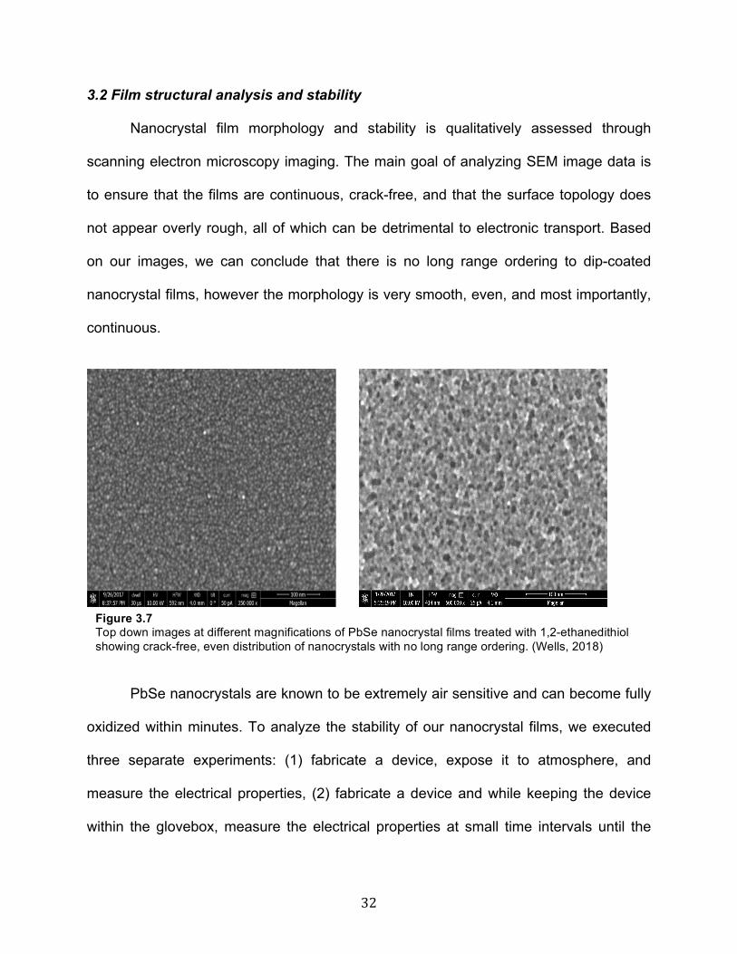
3.2 Film structural analysis and stability
Nanocrystal film morphology and stability is qualitatively assessed through
scanning electron microscopy imaging. The main goal of analyzing SEM image data is
to ensure that the films are continuous, crack-free, and that the surface topology does
not appear overly rough, all of which can be detrimental to electronic transport. Based
on our images, we can conclude that there is no long range ordering to dip-coated
nanocrystal films, however the morphology is very smooth, even, and most importantly,
continuous.
PbSe nanocrystals are known to be extremely air sensitive and can become fully
oxidized within minutes. To analyze the stability of our nanocrystal films, we executed
three separate experiments: (1) fabricate a device, expose it to atmosphere, and
measure the electrical properties, (2) fabricate a device and while keeping the device
within the glovebox, measure the electrical properties at small time intervals until the
Figure 3.7 Top down images at different magnifications of PbSe nanocrystal films treated with 1,2-ethanedithiol showing crack-free, even distribution of nanocrystals with no long range ordering. (Wells, 2018)

33
properties significantly decay, (3) fabricate a device, deposit alumina to infill and
overcoat the film, measure the electrical properties, expose it to atmosphere for
extended periods of time, and re-measure the electrical properties. From these
experiments, we are able to conclude that the as-made nanocrystal films oxidize
immediately upon exposure to air and the as-made nanocrystal films have an
approximate life-time of one hour when kept within the glovebox. However, the alumina
infilled and overcoated devices show no signs of degradation even after being kept in
atmosphere for months to years. From the device fabrication process, we learned that
PbSe nanocrystal films are highly sensitive to deposition methodology. The type of
deposition procedure (drop casting, spin coating, and dip coating) has a large effect on
film morphology, which, in turn, has a large effect on charge transport properties. The
ligand exchange process is very sensitive and requires the nanocrystals not to be over-
treated or under-treated, which can result in incomplete ligand exchange thus affecting
charge transport properties. The environment in which device fabrication and testing is
done is also extremely important due to the reactivity of PbSe nanocrystals with oxygen.
However, sufficient alumina overcoating (~150 cycles or ~20 nm) can prevent oxidation
risk of the nanocrystals and long-term air-stable thermoelectric devices have been
fabricated using this method.[41]

34
3.3 Electrical Behavior
Electrical behavior of our nanocrystal films was characterized through field-effect
transistor measurements on our three-channel silicon substrates with thermal gate
oxide. Measurements were taken before and after atomic layer deposition to capture the
changes to behavior that occurred during the alumina infilling and overcoating process.
Figure 3.9 Bias-stress effect showing transient behavior on linear (left) and log (right) scales with pre-ALD (blue) and post-ALD (green) data.
Figure 3.8 Cross-sectional view of field-effect transistor and thermoelectric substrates showing the flat layers of PbSe nanocrystals and alumina overcoating. (Wells, 2018)

35
The bias-stress effect is known to occur in lead chalcogenide nanomaterials and
heavily affects charge transport behavior in these materials.[42] The bias-stress effect
causes the drain current magnitude to quickly drop, in an Arrhenius fashion, upon
applying a gate bias as shown in figure 3.9. Although the exact origin and mechanism of
this effect is unknown, it is hypothesized to occur due to trap states on the surfaces of
nanocrystals. This effect is noticeably seen in the IV curve through the exponential
Figure 3.10 Pre-ALD field-effect transistor behavior of PbSe nanocrystal film devices. Left image shows positive gate bias IV curve and right image shows positive gate bias transconductance curve.
Figure 3.11 Post-ALD field-effect transistor behavior of PbSe nanocrystal film devices. Left image shows positive gate bias IV curve and right image shows positive gate bias transconductance curve.

36
growth-like curve portion of each gate bias in figure 3.10. It was found that the
magnitude of the bias-stress effect could be significantly reduced if a large negative
gate bias was applied for a period of time before scanning IV, transconductance, and
transient curves in the positive gate bias region. We are also unsure of why this effect
occurs, although we hypothesize that the large opposite pole gate bias may cause large
amounts of trapped opposite charges, which then causes the bias-stress effect to delay.
However, the Law group at University of California, Irvine has been able to significantly
reduce or eliminate the transient effects through atomic layer deposition.[41] The
mechanism is still unknown, although hypothesized to arise from alleviating trap states
in nanocrystals. Aside from the bias-stress effect, our electrical behavior data shows
that we have a mainly electron transport dominated device with some ambipolar
characteristics and that the gate bias works well in increasing drain current magnitudes.
These characteristics lead us to believe that we have a well performing semiconductor
thin film device that can be characterized for thermopower.
3.4 Thermoelectric Behavior
Thermoelectric behavior of our nanocrystalline films was characterized through
Seebeck voltage measurements on our single channel silicon substrates with thermal
gate oxide. A significant portion of this project was to build and qualify a thermopower
testing platform that can be integrated into the electrical testing station housed within a
glovebox. Although all thermopower measurement systems have similar components, it
was not a trivial task due to much of the literature on thermopower measurements
having methods of thermoelectric behavior testing unique to specific research groups.

37
The thermopower measurement station was created to integrate seamlessly with
the current homemade electrical testing station that is equipped with a camera and four
micromanipulator probes. The structure of the thermopower measurement station has
two high-purity copper towers attached to a split base with sliders to adjust the distance
between the two copper towers, which has been set to a default distance of 1 cm. This
split base can be completely detached and reattached by screws onto an electrical
testing aluminum platform. Thermoelectric resistive heating pads, driven by a dedicated
Keithley SMU, are cemented to the tops of the copper towers in order to independently
control the temperature of each tower. Substrates are typically fixed onto the resistive
heating pads using a small amount of silver paste in order to prevent movement during
probing and allow for even heat transport between the substrate and the heating pads.
A separate, optional tower, that is height adjustable, with a homemade integrated
thermocouple Teflon block head, driven by a J-KEM temperature controller, can be
mounted next to the copper towers to allow for quick estimates of temperature by
contacting the block head to the substrate. In order to take accurate temperature
measurements, the micromanipulator probes must be used in conjunction with the lock-
in amplifier. The thermopower measurement station must also be housed within the
glovebox, so dedicated electrical cable lines are connected to outer house of the
glovebox and further split within the glovebox. Due to noise problems caused by
electromagnetic induction effects and long electrical connection lengths, a removable
homemade Faraday cage was built to fit over the electrical and thermopower testing
stations.

38
This homebuilt measurement system has allowed us to characterize our
nanocrystal film devices with minimal transport and oxidation risk in order to obtain the
most accurate data. With this system, we are able to dynamically measure the Seebeck
voltage, or the voltage difference between source and drain electrodes, coupled with
accurate temperature increments driven by heating pads.
Figure 3.12 Schematic (left) and picture (right) of the home built thermopower measurement system. (Wells, 2018)
Figure 3.13 Diagram (left) of a temperature measurement set-up and equation (right) to calculate the temperature from the resistance of our contact metal. (Wells, 2018)

39
In order to establish and qualify our measurement system, we performed
thermopower measurements on four silicon standards with known resistivities, two of
which are p-doped and two of which are n-doped. Due to the geometry of electrical
contacts on our standard samples, only rough estimates of temperature are available to
be measured by a J-KEM temperature controller with thermocouple probes. The
Figure 3.14 (Top)Seebeck coefficient graphs of silicon standard samples. X axis shows the temperature gradient measured, Y-axis shows the Seebeck voltage measured, and the slope of the best-fit-line shows the Seebeck coefficient in V/K. (Bottom) Compiled table of dopant type, resistivities, and Seebeck coefficient of standards.
Standard Dopant Type Resistivity Seebeck Coefficient1 P 0.001-0.005 (ohm*cm)-1 400 µV/K2 P 10-20 (ohm*cm)-1 1100 µV/K3 N 0-100 (ohm*cm)-1 -700 µV/K4 N 320-480 (ohm*cm)-1 -1200 µV/K

40
purpose of this qualification test is to confirm that our measurement system can output
the correct sign and magnitude of the measured Seebeck voltage. From our data, we
can conclude that our measurement system does record the sign and magnitude of the
Seebeck voltage correctly for all of the standard samples.
Figure 3.15 Example graphs of raw data plots for pre-ALD (top two graphs) and post-ALD (bottom two graphs) PbSe nanocrystal film thermoelectric devices.

41
Figure 3.16 Example graphs of calculated Seebeck coefficient and temperature difference values of two pre-ALD PbSe nanocrystal film thermoelectric devices.
Figure 3.17 Example graphs of calculated Seebeck coefficient and temperature difference values of two post-ALD PbSe nanocrystal film thermoelectric devices.

42
The thermoelectric behavior of our PbSe nanocrystal films show much higher
magnitudes of Seebeck coefficient values compared to previous works[43,44,45,46] before
atomic layer deposition (ALD), however those magnitudes typically reduce by 25-50%
after alumina ALD. Because the Seebeck coefficient has an inverse relationship with
carrier concentration and carrier mobility, it is expected that we see a drop in our
Seebeck voltage measurements. However, this does not necessarily mean that the
alumina ALD creates a poor thermoelectric device, due to the order of magnitude
increase in electrical conductivity that occurs from the alumina infilling. The Seebeck
coefficient may be halved causing the power factor to be cut by 3/4, however the order
of magnitude increase in electrical conductivity causes the overall power factor to
increase. It was found that the pre-ALD Seebeck coefficient is around 1500-2000 µV/K,
while the post-ALD Seebeck coefficient is around 800-1200 µV/K. The pre-ALD
conductivity is around 0.001 to 0.01 S/cm, while the post-ALD conductivity is around
0.01 to 0.1 S/cm. This gives the post-ALD power factor an overall increase of around 2-
3 times the pre-ALD power factor. Although the power factor isn’t exhibiting an
enormous increase, the alumina infilling and overcoating creates a shield for the
nanocrystal film making the film air-stable over months or even years.
We have shown during this project that we can reliably measure thermopower in
thermoelectric materials with our current unique measurement system. Typical
thermoelectric measurement set-ups utilize thermocouples as temperature monitors, do
not allow for optimal heat conduction away from the substrate, and cannot efficiently
test small substrate sizes. Our novel thermoelectric measurement station utilizes ultra
high purity copper stands to effectively remove heat in order to establish a large, stable

43
temperature gradient. Temperature measurements are taken more accurately than
using thermocouples by using the lock-in amplifier to measure the resistance of a gold
lead and using that resistance to back-calculate the temperature. The separation
distance between the hot stack and cold stack is typically set to 1 cm, however the base
is mounted on an adjustable platform that can be set between a few millimeters of
separation to several inches of separation. It was also found to be extremely sensitive to
noise and interference from electromagnetic radiation, so we constructed homemade
aluminum Faraday cage shell to fit over the entire thermoelectric measurement and
probe station. Our results show that PbSe nanocrystal films exhibit high Seebeck
coefficient values that decrease upon alumina atomic layer deposition, but also have a
noticeable increase in overall power factor. Alumina infilling by atomic layer deposition
is confirmed to significantly improve the electrical properties of PbSe nanocrystalline
thin films. The exact mechanism is still unknown, however, it is hypothesized to be due
to the alumina alleviating surface charge trap states and/or also preventing ion transport
within the film, which may significantly increase effective charge carrier concentration,
charge mobility, or both. The electrical properties of the nanocrystal films are improved,
however, the Seebeck coefficient decreases by about a factor of 2 after ALD treatment.
4. Conclusion
We investigated the thermoelectric properties of lead selenide nanocrystal films
and to have maximum control in device performance, we began with the optimization of
the nanocrystal synthesis and device fabrication from as-bought precursor materials. In
this work, we set to establish a new thermopower measurement system within a
glovebox to measure thin film devices before and after atomic layer deposition

44
treatment without the risk of oxidation. To qualify our system, we characterized a variety
of silicon chip standards with known resistivities and charge carrier type, which all
showed correct trends in Seebeck coefficient signs and magnitudes. We also show, in
of our PbSe nanocrystal devices, large Seebeck coefficient values prior to atomic layer
deposition treatment and diminished Seebeck coefficient values post treatment. Our
thermoelectric data indicates that the Seebeck coefficient values typically decrease by a
factor of 2, whereas our electrical data indicate that conductivity values typically
increase by a factor of 10 with treatment. Overall, the power factor of our material
increases by a factor of 2-3 with treatment. However, the origin of this increase is still
unknown and might arise from an increased mobility contribution or from an increased
charge carrier concentration. The mechanism of the treatment that causes the increase
charge mobility and effective charge concentration is also not completely understood,
but may be due to passivation of surface trap states. Further studies must be done in
order to fully understand the thermoelectric behavior and outlook of these materials in
applications.
Thermoelectric materials have had a relatively brief history and constant emerging
improvements have been made to the performance of thermoelectric devices. In recent
years, lab thermoelectric data have seen several-fold increases in ZT along with many
emerging start-up companies working to produce consumer thermoelectric devices.[48] I
hope that the results from this project will aid in the advancement of thermoelectric
materials and that one day thermoelectric materials will be able to make a real impact in
the world’s energy crisis.

45
5. Future Work
I believe that this project was only the tip of the iceberg for lead selenide
nanocrystalline thermoelectrics and hope that much more work can be done on lead
chalcogenide nanomaterial thermoelectric devices. For future advancements, I would
like to see the following:
1) For nanocrystal synthesis, a combinations of sizes and compositions should be
tested to optimize the perfect nanocrystal thin film morphology and energy
filtering performance.
2) Although a lot of work has been put towards optimizing device fabrication
conditions, I believe that a few more slight modifications to film deposition
conditions could improve the behavior slightly or produce more stable behavior
and reduce variation from device to device. Such modifications may include
higher resolution adjustments of ligand exchange solution concentration,
nanocrystal concentration, substrate pattern adjustments, dip coating speed/time,
and spin coating speed/time.
3) Working with 1,2-ethanedithiol as a ligand and alumina as an atomic layer
deposition infilling material are good starting points for developing high
performance PbSe nanocrystalline thermoelectric devices due to the amount of
literature and research on these materials. However, it would also be worth
testing other ligands and atomic layer deposition materials that are thought to
improve performance such as thiocyanate ligands and titanium oxide or hafnium
oxide ALD infilling.

46
4) Our current thermoelectric measurement set-up can accurately take
measurements with microvolt precision and is more than enough resolution for
the current state of the project. However, I believe that the measurement station
can be further optimized by reducing the amount of noise signal from many
sources.
5) The culmination of the project would be assembling and packaging the PbSe
nanocrystalline devices into a working thermoelectric generator or thermoelectric
heater/cooler, however much more development would need to be done before
the efficiency can be comparable to those on the current consumer market.
I hope that with this project, I could push the current state of nanoscale thermoelectrics
further towards the ultimate goal of producing cost-efficient waste heat generators. I
believe that this ultimate goal would be able to amend some of the world’s energy
concerns and would aid in the current mission of humanity in moving towards cleaner
sources of energy for a greener Earth.

47
6. References
[1] Vining, C. B. (2009, February 1). An inconvenient truth about thermoelectrics [Comments and Opinion]. https://doi.org/10.1038/nmat2361
[2] Hochbaum, A. I., Chen, R., Delgado, R. D., Liang, W., Garnett, E. C., Najarian, M., Yang, P. (2008). Enhanced thermoelectric performance of rough silicon nanowires. Nature, 451(7175), 163–167. https://doi.org/10.1038/nature06381
[3] Seebeck, Th. J. "Magnetische Polarisation der Metalle und Erze Durch Temperatur-Differenz"1822-23 in Ostwald's Klassiker der Exakten Wissenshaften Nr. 70 (1895). Seebeck Biography 1. Seebeck Biography 2.
[4] Magnus, G. Poggendorf's Annalen der Physik 83 p469 (1851) [5] Thomson, W. "On the Dynamical Theory of Heat. Trans." R. Soc. Edinburgh:
Earth Sci. 3, 91–98 (1851). Thomson Biography. [6] Snyder, G. J. (2018). Thermoelectrics: Northwestern Materials Science and
Engineering. Retrieved May 9, 2018, from http://thermoelectrics.matsci.northwestern.edu/
[7] Altenkirch, E. Physikalische Zeitschrift 10, 560–580 (1909); Physikalische Zeitschrift 12, 920 (1911)
[8] Eucken, A. and Kuhn, G. Z. Phys. Chem. 134 p193 (1928) [9] Heikes, R.R. and Ur, R.W. "Thermoelectricity: Science and Engineering"
Interscience Publishers, (1961); I. B. Cadoff and E. Miller "Thermoelectric Materials and Devices" Materials Technology Series. Reinhold Publishing Cooperation (1960); P. H. Egli "Thermoelectricity" John Wiley & Sons (1960)
[10] Vedernikov, M.V. and Iordanishvili, E.K. "A. F. Ioffe and origin of modern semiconductor thermoelectric energy conversion" 17th Int. Conf. on Thermoelectrics vol 1, pp 37–42 (1998); A. F. Ioffe "Semiconductor Thermoelements and Thermoelectric Cooling"
[11] Goldsmid, H.J. and Douglas, R.W. "The use of semiconductors in thermoelectric refrigeration" British J. Appl. Phys. 5, 386 (1954)
[12] Glen Slack in CRC Handbook of Thermoelectrics (ed. Rowe, M.) p407–440 (1995).
[13] Bell, L. "Cooling, Heating, Generating Power, and Recovering Waste Heat with Thermoelectric Systems" Science Vol. 321. pp. 1457 (2008)
[14] Snyder, G.J. and Toberer, E. "Complex Thermoelectric Materials" Nature Materials 7, 105-114 (2008)
[15] Dresselhaus, M.S. et al. "New directions for low-dimensional thermoelectric materials" Adv. Mater. 19, 1043–1053 (2007); M. G. Kanatzidis "Nanostructured thermoelectrics: the new paradigm?" Chem. Mater. 22, 648–659 (2010)
[16] Wood, C. (1988). Materials for thermoelectric energy conversion. Reports on Progress in Physics, 51(4), 459. https://doi.org/10.1088/0034-4885/51/4/001
[17] GHI - Institut für Gesteinshüttenkunde der RWTH-Aachen. (n.d.). Retrieved May 13, 2018, from https://www.ghi.rwth-aachen.de/simulation
[18] Silicon crystal structure and defects. - ppt video online download. (n.d.). Retrieved May 13, 2018, from http://slideplayer.com/slide/4645797/#
[19] Biswas, K., He, J., Blum, I. D., Wu, C.-I., Hogan, T. P., Seidman, D. N., … Kanatzidis, M. G. (2012). High-performance bulk thermoelectrics with all-scale

48
hierarchical architectures. Nature, 489(7416), 414–418. https://doi.org/10.1038/nature11439
[20] Quantum Dots. (n.d.). Retrieved May 13, 2018, from https://www.sigmaaldrich.com/technical-documents/articles/materials-science/nanomaterials/quantum-dots.html
[21] Hochbaum, A. I., Chen, R., Delgado, R. D., Liang, W., Garnett, E. C., Najarian, M., Yang, P. (2008). Enhanced thermoelectric performance of rough silicon nanowires. Nature, 451(7175), 163–167. https://doi.org/10.1038/nature06381
[22] Boukai, A. I., Bunimovich, Y., Tahir-Kheli, J., Yu, J.-K., Iii, W. A. G., & Heath, J. R. (2008). Silicon nanowires as efficient thermoelectric materials. Nature, 451(7175), 168–171. https://doi.org/10.1038/nature06458
[23] Nanocrystal self-assembly sheds its secrets. (n.d.). Retrieved May 14, 2018, from http://news.mit.edu/2016/self-assembly-nanocrystals-sheds-secrets-0321
[24] Harman, T. C., Taylor, P. J., Walsh, M. P., & LaForge, B. E. (2002). Quantum Dot Superlattice Thermoelectric Materials and Devices. Science, 297(5590), 2229–2232. https://doi.org/10.1126/science.1072886
[25] Bulman, G., Barletta, P., Lewis, J., Baldasaro, N., Manno, M., Bar-Cohen, A., & Yang, B. (2016). Superlattice-based thin-film thermoelectric modules with high cooling fluxes. Nature Communications, 7, 10302. https://doi.org/10.1038/ncomms10302
[26] Zhang, Y., Chen, Y., Gong, C., Yang, J., Qian, R., & Wang, Y. (2007). Optimization of Superlattice Thermoelectric Materials and Microcoolers. Journal of Microelectromechanical Systems, 16(5), 1113–1119. https://doi.org/10.1109/JMEMS.2007.900884
[27] Thermocouple Temperature Sensors, how they work, color codes, recommended limits, limits of accuracy, calibration tables, vendor links and more. (n.d.). Retrieved June 7, 2018, from https://www.temperatures.com/tcs.html
[28] Thermoelectric materials - Smart Material. (n.d.). Retrieved May 13, 2018 [29] Zhang, G. Nanowire Applications: Thermoelectric Cooling and Energy
Harvesting: INTECH Open Access Publisher, 2011. [30] Fylladitakis, E. The Phononic HEX 2.0 TEC CPU Cooler Review. Retrieved May
14, 2018, from https://www.anandtech.com/show/10695/the-phononic-hex-2-0-tec-cpu-cooler-review
[31] Zhou, Y., Paul, S., & Bhunia, S. (2008). Harvesting Wasted Heat in a Microprocessor Using Thermoelectric Generators: Modeling, Analysis and Measurement. In 2008 Design, Automation and Test in Europe (pp. 98–103). https://doi.org/10.1109/DATE.2008.4484669
[32] Glosch, H., Ashauer, M., Pfeiffer, U., & Lang, W. (1999). A thermoelectric converter for energy supply. Sensors and Actuators A: Physical, 74(1), 246–250. https://doi.org/10.1016/S0924-4247(98)00298-2
[33] Orr, B., Akbarzadeh, A., Mochizuki, M., & Singh, R. (2016). A review of car waste heat recovery systems utilising thermoelectric generators and heat pipes. Applied Thermal Engineering, 101, 490–495. https://doi.org/10.1016/j.applthermaleng.2015.10.081

49
[34] Kraemer, D., Hu, L., Muto, A., Chen, X., Chen, G., & Chiesa, M. (2008). Photovoltaic-thermoelectric hybrid systems: A general optimization methodology. Applied Physics Letters, 92(24), 243503. https://doi.org/10.1063/1.2947591
[35] Kagan, C. R., Lifshitz, E., Sargent, E. H., & Talapin, D. V. (2016). Building devices from colloidal quantum dots. Science, 353(6302), aac5523. https://doi.org/10.1126/science.aac5523
[36] Law, M., Luther, J. M., Song, Q., Hughes, B. K., Perkins, C. L., & Nozik, A. J. (2008). Structural, Optical, and Electrical Properties of PbSe Nanocrystal Solids Treated Thermally or with Simple Amines. Journal of the American Chemical Society, 130(18), 5974–5985. https://doi.org/10.1021/ja800040c
[37] Liu, Y., Gibbs, M., Puthussery, J., Gaik, S., Ihly, R., Hillhouse, H. W., & Law, M. (2010). Dependence of Carrier Mobility on Nanocrystal Size and Ligand Length in PbSe Nanocrystal Solids. Nano Letters, 10(5), 1960–1969. https://doi.org/10.1021/nl101284k
[38] Murphy, J. E., Beard, M. C., Norman, A. G., Ahrenkiel, S. P., Johnson, J. C., Yu, P., Nozik, A. J. (2006). PbTe Colloidal Nanocrystals: Synthesis, Characterization, and Multiple Exciton Generation. Journal of the American Chemical Society, 128(10), 3241–3247. https://doi.org/10.1021/ja0574973
[39] CdSe_nanocrystal_growth.jpg (2963×900). Retrieved May 19, 2018, from https://upload.wikimedia.org/wikipedia/commons/5/57/CdSe_nanocrystal_growth.jpg
[40] Talapin, D. V., & Murray, C. B. (2005). PbSe Nanocrystal Solids for n- and p-Channel Thin Film Field-Effect Transistors. Science, 310(5745), 86–89. https://doi.org/10.1126/science.1116703
[41] Liu, Y., Tolentino, J., Gibbs, M., Ihly, R., Perkins, C. L., Liu, Y., Law, M. (2013). PbSe Quantum Dot Field-Effect Transistors with Air-Stable Electron Mobilities above 7 cm2 V–1 s–1. Nano Letters, 13(4), 1578–1587. https://doi.org/10.1021/nl304753n
[42] Osedach, T. P., Zhao, N., Andrew, T. L., Brown, P. R., Wanger, D. D., Strasfeld, D. B., Bulović, V. (2012). Bias-Stress Effect in 1,2-Ethanedithiol-Treated PbS Quantum Dot Field-Effect Transistors. ACS Nano, 6(4), 3121–3127. https://doi.org/10.1021/nn3008788
[43] Kogo, G., Pradhan, A. K., & Roy, U. N. (2017). Thermoelectric Behavior of PbSe Single Crystals. ECS Journal of Solid State Science and Technology, 6(3), N3006–N3009. https://doi.org/10.1149/2.0021703jss
[44] Liang, W., Rabin, O., Hochbaum, A. I., Fardy, M., Zhang, M., & Yang, P. (2009). Thermoelectric properties of p-type PbSe nanowires. Nano Research, 2(5), 394–399. https://doi.org/10.1007/s12274-009-9039-2
[45] Parker, D., Singh, D. J., Zhang, Q., & Ren, Z. (2012). Thermoelectric properties of n-type PbSe revisited. Journal of Applied Physics, 111(12), 123701. https://doi.org/10.1063/1.4728229
[46] Wang, R. Y., Feser, J. P., Lee, J.-S., Talapin, D. V., Segalman, R., & Majumdar, A. (2008). Enhanced Thermopower in PbSe Nanocrystal Quantum Dot Superlattices. Nano Letters, 8(8), 2283–2288. https://doi.org/10.1021/nl8009704
[47] Urban, J. J. (2015, December 3). Prospects for thermoelectricity in quantum dot hybrid arrays [Comments and Opinion]. https://doi.org/10.1038/nnano.2015.289

50
[48] Vining, C. B. (2009, February 1). An inconvenient truth about thermoelectrics [Comments and Opinion]. https://doi.org/10.1038/nmat2361
[49] Majumdar, A. (2004). Thermoelectricity in Semiconductor Nanostructures. Science, 303(5659), 777–778. https://doi.org/10.1126/science.1093164
[50] Young, D. L., Coutts, T. J., & Kaydanov, V. I. (2000). Density-of-states effective mass and scattering parameter measurements by transport phenomena in thin films. Review of Scientific Instruments, 71(2), 462–466. https://doi.org/10.1063/1.1150224
[51] Wang, R. (2017). Thermoelectric Thin Films and Nanocomposites Synthesized Via Solution-Phase Chemistry. Meeting Abstracts, MA2017-02(27), 1180–1180.
[52] Venkatasubramanian, R., Siivola, E., Colpitts, T., & O’Quinn, B. (2001). Thin-film thermoelectric devices with high room-temperature figures of merit. Nature, 413(6856), 597–602. https://doi.org/10.1038/35098012
[53] Ding, D., Wang, D., Zhao, M., Lv, J., Jiang, H., Lu, C., & Tang, Z. (n.d.). Interface Engineering in Solution-Processed Nanocrystal Thin Films for Improved Thermoelectric Performance. Advanced Materials, 29(1), 1603444. https://doi.org/10.1002/adma.201603444
[54] Choi, J., Cho, K., Yun, J., Park, Y., Yang, S., & Kim, S. (n.d.). Large Voltage Generation of Flexible Thermoelectric Nanocrystal Thin Films by Finger Contact. Advanced Energy Materials, 7(21), 1700972. https://doi.org/10.1002/aenm.201700972
[55] Lynch, J., Kotiuga, M., Doan-Nguyen, V. V. T., Queen, W. L., Forster, J. D., Schlitz, R. A., … Urban, J. J. (2014). Ligand Coupling Symmetry Correlates with Thermopower Enhancement in Small-Molecule/Nanocrystal Hybrid Materials. ACS Nano, 8(10), 10528–10536. https://doi.org/10.1021/nn503972v
[56] Zhang, Y., & Stucky, G. D. (2014). Heterostructured Approaches to Efficient Thermoelectric Materials. Chemistry of Materials, 26(1), 837–848. https://doi.org/10.1021/cm402150j