


DescriptionThe Allegro® A8735 is a Xenon photoflash charger IC designed to meet the needs of ultra low power, small form factor cameras, particularly camera phones. By using primary-side voltage sensing, the need for a secondary-side resistive voltage divider is eliminated. This has the additional benefit of reducing leakage currents on the secondary side of the transformer. To extend battery life, the A8735 features very low supply current draw (0.5 たA max in shutdown mode). The IGBT driver also has internal gate resistors for minimum external component count. The charge and trigger voltage logic thresholds are set at 1 VHI(min) to support applications implementing low-voltage control logic.
The A8735 is available in an 8-contact 2 mm × 2 mm DFN/MLP package with a 0.60 maximum overall package height, and an exposed pad for enhanced thermal performance. It is lead (Pb) free with 100% matte tin leadframe plating.
8735-DS
Features and Benefitsザ Ultra small 2 × 2 DFN/MLP-8 packageザ Low quiescent current draw (0.5 たA max. in shutdown mode)ザ Primary-side output voltage sensing; no resistor divider requiredザ Fixed 1 A peak current limitザ 1V logic (VHI(min)) compatibilityザ Integrated IGBT driver with internal gate resistorsザ Optimized for mobile phone, 1-cell Li+ battery applicationsザ Zero-voltage switching for lower lossザ >75% efficiencyザ Charge complete indicationザ Integrated 50 V DMOS switch with self-clamping protection
Ultra Small Mobile Phone Xenon Photoflash Capacitor Charger with IGBT Driver
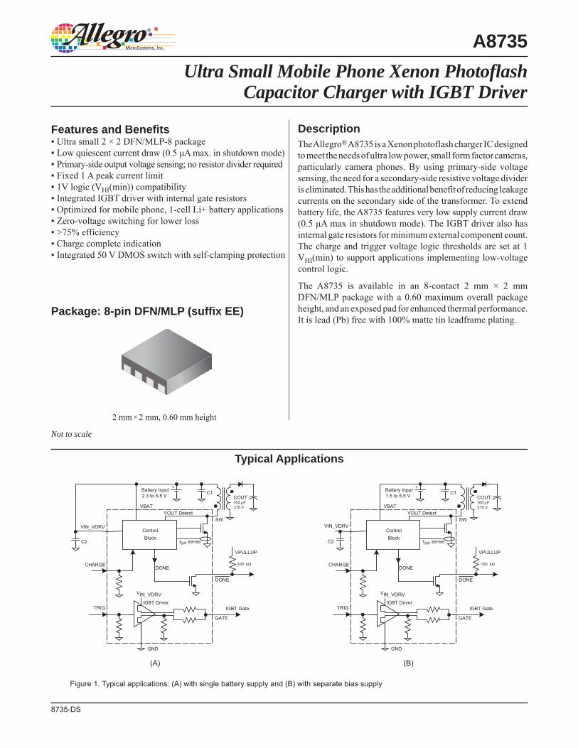
Package: 8-pin DFN/MLP (suffix EE)
Typical Applications
Not to scale
A8735
2 mm × 2 mm, 0.60 mm height
+
SW
VBAT
VIN_VDRV
Control
Block
CHARGE
VIN_VDRV
DONE
GND
TRIG
VPULLUP
VOUT Detect
ISW sense
DONE
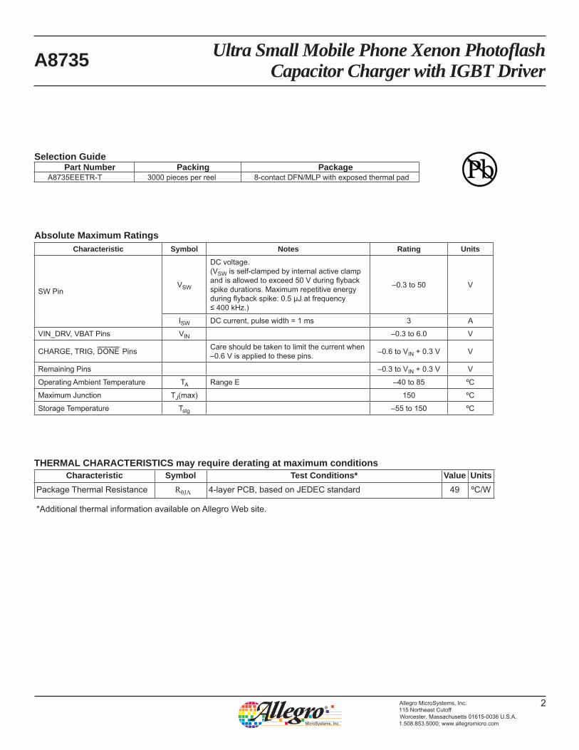
Battery Input2.3 to 5.5 V
C2
COUT100F315 V
C1
100 kΩ
IGBT Gate
GATE
IGBT Driver
+
SW
VBAT
VIN_VDRV
Control
Block
CHARGE
VIN_VDRV
DONE
GND
TRIG
VPULLUP
VOUT Detect
ISW sense
DONE
Battery Input1.5 to 5.5 V
C2
COUT100F315 V
C1
100 kΩ
IGBT Gate
GATE
IGBT Driver
Figure 1. Typical applications: (A) with single battery supply and (B) with separate bias supply
(A) (B)
Ultra Small Mobile Phone Xenon Photoflash Capacitor Charger with IGBT Driver
2Allegro MicroSystems, Inc.115 Northeast CutoffWorcester, Massachusetts 01615-0036 U.S.A.1.508.853.5000; www.allegromicro.com
A8735
Selection GuidePart Number Packing Package
A8735EEETR-T 3000 pieces per reel 8-contact DFN/MLP with exposed thermal pad
Absolute Maximum RatingsCharacteristic Symbol Notes Rating Units
SW PinVSW
DC voltage.(VSW is self-clamped by internal active clamp and is allowed to exceed 50 V during flyback spike durations. Maximum repetitive energy during flyback spike: 0.5 μJ at frequency ≤ 400 kHz.)
–0.3 to 50 V
ISW DC current, pulse width = 1 ms 3 A
VIN_DRV, VBAT Pins VIN –0.3 to 6.0 V
CHARGE, TRIG, D O N E PinsCare should be taken to limit the current when –0.6 V is applied to these pins.
–0.6 to VIN + 0.3 V V
Remaining Pins –0.3 to VIN + 0.3 V V
Operating Ambient Temperature TA Range E –40 to 85 ºC
Maximum Junction TJ(max) 150 ºC
Storage Temperature Tstg –55 to 150 ºC
THERMAL CHARACTERISTICS may require derating at maximum conditionsCharacteristic Symbol Test Conditions* Value Units
Package Thermal Resistance RしJA 4-layer PCB, based on JEDEC standard 49 ºC/W
*Additional thermal information available on Allegro Web site.
Ultra Small Mobile Phone Xenon Photoflash Capacitor Charger with IGBT Driver
3Allegro MicroSystems, Inc.115 Northeast CutoffWorcester, Massachusetts 01615-0036 U.S.A.1.508.853.5000; www.allegromicro.com
A8735
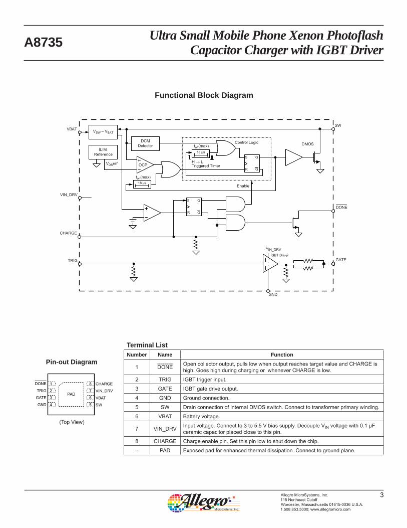
Functional Block Diagram
VBATSW
GND
OCP
CHARGE
VDSref
ton(max)
toff(max)
DONE
TRIG
VIN_DRV
DMOS
VSW – VBAT
Q
QS
R
Q
QS
R
DCMDetector
ILIM Reference
H LTriggered Timer
Control Logic
18 μs
18 μsEnable
VIN_DRV
IGBT Driver
GATE
Pin-out Diagram
(Top View)
DONE
TRIG
GATE
GND
CHARGE
VIN_DRV
VBAT
SW
PAD
1
2
3
4
8
7
6
5
Terminal ListNumber Name Function
1 D O N E Open collector output, pulls low when output reaches target value and CHARGE is high. Goes high during charging or whenever CHARGE is low.
2 TRIG IGBT trigger input.
3 GATE IGBT gate drive output.
4 GND Ground connection.
5 SW Drain connection of internal DMOS switch. Connect to transformer primary winding.
6 VBAT Battery voltage.
7 VIN_DRVInput voltage. Connect to 3 to 5.5 V bias supply. Decouple VIN voltage with 0.1 たF ceramic capacitor placed close to this pin.
8 CHARGE Charge enable pin. Set this pin low to shut down the chip.
– PAD Exposed pad for enhanced thermal dissipation. Connect to ground plane.
Ultra Small Mobile Phone Xenon Photoflash Capacitor Charger with IGBT Driver
4Allegro MicroSystems, Inc.115 Northeast CutoffWorcester, Massachusetts 01615-0036 U.S.A.1.508.853.5000; www.allegromicro.com
A8735
ELECTRICAL CHARACTERISTICS Typical values are valid at VIN = VBAT = 3.6 V; TA = 25°C, except indicates specifications guaranteed from −40°C to 85°C ambient, unless otherwise noted
Characteristics Symbol Test Conditions Min. Typ. Max. Unit
VBAT Voltage Range1 VBAT 1.5 – 5.5 V
VIN_DRV Voltage Range1 VIN 2.3 – 5.5 V
UVLO Enable Threshold VINUV VIN rising – 2.05 2.2 V
UVLO Hysteresis VINUV(hys) – 150 – mV
VIN Supply Current IIN
Shutdown (CHARGE = 0 V, TRIG = 0 V) – 0.02 0.5 たA
Charging complete – 50 100 たA
Charging (CHARGE = VIN, TRIG = 0 V) – 2 – mA
VBAT Pin Supply Current IBAT
Shutdown (CHARGE = 0 V, TRIG = 0 V) – 0.01 1 たA
Charging done (CHARGE = VIN, D O N E = 0 V)
– – 5 たA
Charging (CHARGE = VIN, TRIG = 0 V) – – 50 たA
Current Limit
Primary-Side Current Limit2 ISWLIM 0.9 1.0 1.1 A
Switch On-Resistance RSWDS(on) VIN_DRV = 3.6 V, ID = 600 mA, TA = 25°C – 0.4 – っ
Switch Leakage Current1 ISWLK VSW = 5.5, over full temperature range – – 2 たA
CHARGE Input Current ICHARGE VCHARGE = VIN – 36 – たA
CHARGE Input Voltage1 VCHARGE High, over input supply range 1.0 – – V
Low, over input supply range – – 0.4 V
CHARGE On/Off Delay tCH Time between CHARGE = 1 and charging enabled
– 20 – us
Switch-Off Timeout toff(max) – 18 – たs
Switch-On Timeout ton(max) – 18 – たs
Output Comparator Trip Voltage3 VOUTTRIP Measured as VSW – VBAT 31.0 31.5 32.0 V
Output Comparator Voltage Overdrive VOUTOV Pulse width = 200 ns (90% to 90%) – 200 400 mV
D O N E Output Leakage Current1 IDONELK 1 μA
D O N E Output Low Voltage1 VDONEL 32 たA into D O N E pin – – 100 mV
dV/dt Threshold for ZVS Comparator dV/dt Measured at SW pin – 20 – V/μs
IGBT Driver
TRIG Input Voltage1 VTRIG(H) Input = logic high, over input supply range 1 – – V
VTRIG(L) Input = logic low, over input supply range – – 0.4 V
TRIG Pull-Down Resistor RTRIGPD – 100 – kっ
GATE Resistance to VIN_DRV RSrcDS(on) VGATE = 1.8 V – 21 – っ
GATE Resistance to GND RSnkDS(on) VGATE = 1.8 V – 27 – っ
Propagation Delay (Rising)4,5 tDr Measurement taken at D O N E pin, CL= 6500 pF
– 25 – ns
Propagation Delay (Falling)4,5 tDf – 60 – ns
Output Rise Time4,5 tr – 290 – ns
Output Fall Time4,5 tf – 380 – ns
GATE Pull-Down Resistor RGTPD – 20 – kっ1Specifications throughout the range TA = –40°C to 85°C guaranteed by design and characterization.2Current limit guaranteed by design and correlation to static test.3Specifications throughout the range TA = –20°C to 85°C guaranteed by design and characterization.4Guaranteed by design and characterization.5See IGBT Drive Timing Definition diagram for further information.
Ultra Small Mobile Phone Xenon Photoflash Capacitor Charger with IGBT Driver
5Allegro MicroSystems, Inc.115 Northeast CutoffWorcester, Massachusetts 01615-0036 U.S.A.1.508.853.5000; www.allegromicro.com
A8735
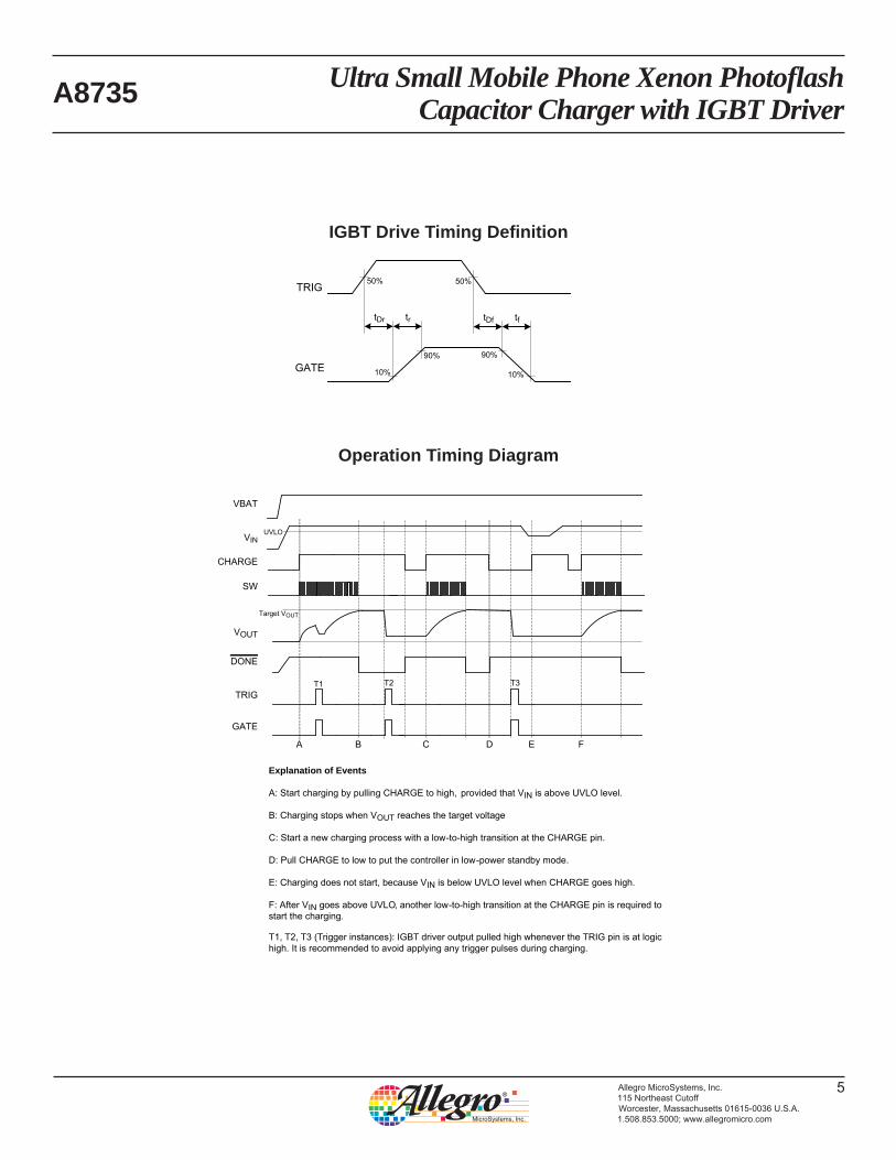
IGBT Drive Timing Definition
GATE
TRIG
tDr tr tDf tf
50%
10%
90%
50%
10%
90%
Operation Timing Diagram
high transition at the CHARGE pin.
VOUT
CHARGE
DONE
VIN
VBAT
TRIG
GATE
SW
A B
Explanation of Events
A: Start charging by pulling CHARGE to high, provided that VIN is above UVLO level. B: Charging stops when VOUT reaches the target voltage. C: Start a new charging process with a low-to-
D: Pull CHARGE to low to put the controller in low-power standby mode. E: Charging does not start, because VIN is below UVLO level when CHARGE goes high.
F: After VIN goes above UVLO, another low-to-high transition at the CHARGE pin is required to start the charging.
UVLO
Target VOUT
C D E F
T3T1 T2
T1, T2, T3 (Trigger instances): IGBT driver output pulled high whenever the TRIG pin is at logic high. It is recommended to avoid applying any trigger pulses during charging.
Ultra Small Mobile Phone Xenon Photoflash Capacitor Charger with IGBT Driver
6Allegro MicroSystems, Inc.115 Northeast CutoffWorcester, Massachusetts 01615-0036 U.S.A.1.508.853.5000; www.allegromicro.com
A8735
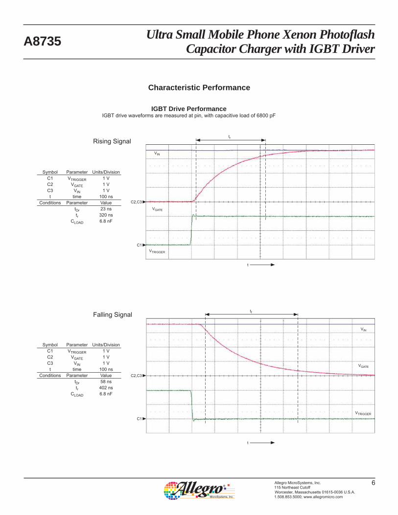
Characteristic Performance
IGBT Drive PerformanceIGBT drive waveforms are measured at pin, with capacitive load of 6800 pF
Rising Signal
Symbol Parameter Units/Division
C1 VTRIGGER 1 V
C2 VGATE 1 V
C3 VIN 1 V
t time 100 ns
Conditions Parameter Value
tDr 23 ns
tr 320 ns
CLOAD 6.8 nF
C1
C2,C3
t
VGATE
VTRIGGER
VIN
tr
Symbol Parameter Units/Division
C1 VTRIGGER 1 V
C2 VGATE 1 V
C3 VIN 1 V
t time 100 ns
Conditions Parameter Value
tDr 58 ns
tr 402 ns
CLOAD 6.8 nF
C1
C2,C3
Falling Signal
VGATE
VIN
VTRIGGER
t
tf
Ultra Small Mobile Phone Xenon Photoflash Capacitor Charger with IGBT Driver
7Allegro MicroSystems, Inc.115 Northeast CutoffWorcester, Massachusetts 01615-0036 U.S.A.1.508.853.5000; www.allegromicro.com
A8735
Characteristic Performance
0
2
4
6
8
10
12
14
16
18
20
1.5 2.0 2.5 3.0 3.5 4.0 4.5 5.0 5.5
Tim
e (
Se
c)
Battery Voltage (V)
54%
56%
58%
60%
62%
64%
66%
68%
70%
72%
74%
76%
78%
80%
82%
84%
86%
1.5 2.0 2.5 3.0 3.5 4.0 4.5 5.0 5.5
Eff
icie
ncy
(%
)
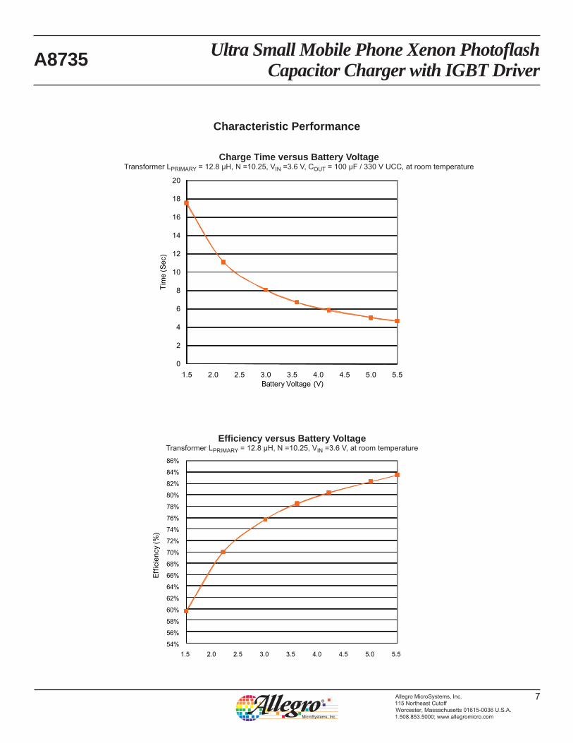
Efficiency versus Battery VoltageTransformer LPRIMARY = 12.8 μH, N =10.25, VIN =3.6 V, at room temperature
Charge Time versus Battery VoltageTransformer LPRIMARY = 12.8 μH, N =10.25, VIN =3.6 V, COUT = 100 μF / 330 V UCC, at room temperature
Ultra Small Mobile Phone Xenon Photoflash Capacitor Charger with IGBT Driver
8Allegro MicroSystems, Inc.115 Northeast CutoffWorcester, Massachusetts 01615-0036 U.S.A.1.508.853.5000; www.allegromicro.com
A8735
320
321
322
323
324
325
326
327
328
1.5 2.0 2.5 3.0 3.5 4.0 4.5 5.0 5.5Battery Voltage (V)
VO
UT (
V)
0.20
0.25
0.30
0.35
0.40
0.45
0.50
1.5 2.0 2.5 3.0 3.5 4.0 4.5 5.0 5.5
Cu
rre
nt
(A)
Battery Voltage (V)
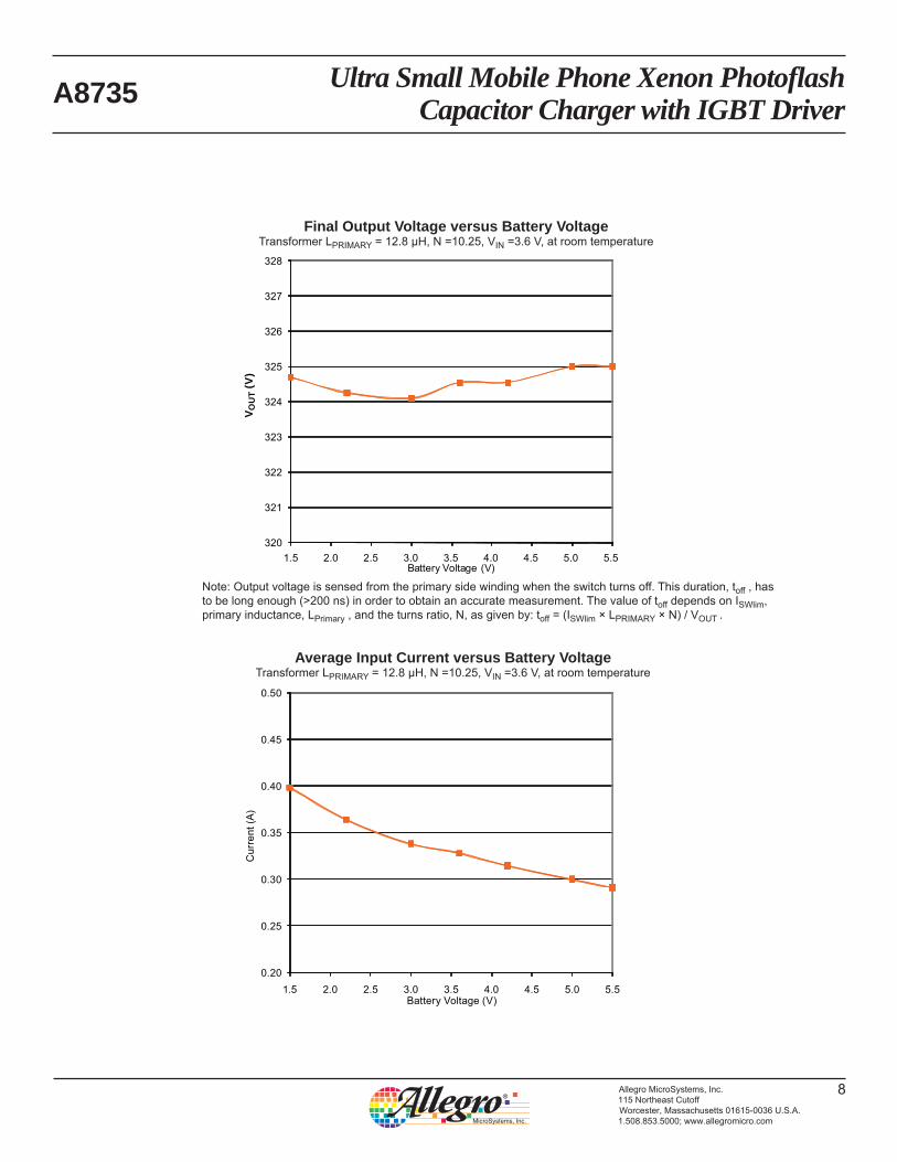
Note: Output voltage is sensed from the primary side winding when the switch turns off. This duration, toff , has to be long enough (>200 ns) in order to obtain an accurate measurement. The value of toff depends on ISWlim, primary inductance, LPrimary , and the turns ratio, N, as given by: toff = (ISWlim × LPRIMARY × N) / VOUT .
Final Output Voltage versus Battery VoltageTransformer LPRIMARY = 12.8 μH, N =10.25, VIN =3.6 V, at room temperature
Average Input Current versus Battery VoltageTransformer LPRIMARY = 12.8 μH, N =10.25, VIN =3.6 V, at room temperature
Ultra Small Mobile Phone Xenon Photoflash Capacitor Charger with IGBT Driver
9Allegro MicroSystems, Inc.115 Northeast CutoffWorcester, Massachusetts 01615-0036 U.S.A.1.508.853.5000; www.allegromicro.com
A8735
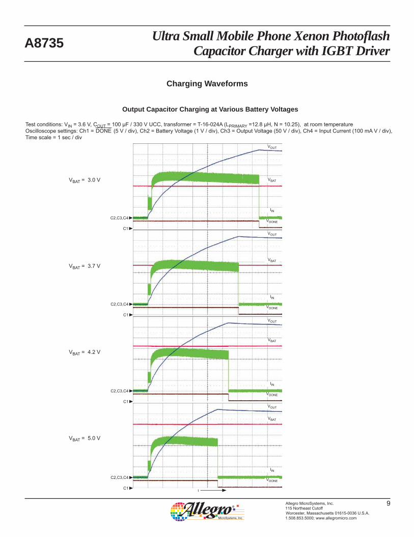
Output Capacitor Charging at Various Battery Voltages
Test conditions: VIN = 3.6 V, COUT = 100 μF / 330 V UCC, transformer = T-16-024A (LPRIMARY =12.8 μH, N = 10.25), at room temperatureOscilloscope settings: Ch1 = D O N E (5 V / div), Ch2 = Battery Voltage (1 V / div), Ch3 = Output Voltage (50 V / div), Ch4 = Input Current (100 mA V / div),Time scale = 1 sec / div
t
C2,C3,C4
C1
VOUT
IIN
VDONE
VBAT
C2,C3,C4
C1
VOUT
IIN
VDONE
VBAT
C2,C3,C4
C1
VOUT
IIN
VDONE
VBAT
VOUT
IIN
VDONE
VBAT
C2,C3,C4
C1
VBAT = 4.2 V
VBAT = 3.7 V
VBAT = 3.0 V
VBAT = 5.0 V
Charging Waveforms
Ultra Small Mobile Phone Xenon Photoflash Capacitor Charger with IGBT Driver
10Allegro MicroSystems, Inc.115 Northeast CutoffWorcester, Massachusetts 01615-0036 U.S.A.1.508.853.5000; www.allegromicro.com
A8735
General Operation OverviewThe charging operation is started by a low-to-high signal on the
CHARGE pin, provided that VIN is above the VUVLO level. It is
strongly recommended to keep the CHARGE pin at logic low
during power-up. After VIN exceeds the UVLO level, a low-
to-high transition on the CHARGE pin is required to start the
charging. The D ¯ O N E open-drain indicator is pulled low when
CHARGE is high and target output voltage is reached.
When a charging cycle is initiated, the transformer primary side
current, IPRIMARY , ramps-up linearly at a rate determined by the
combined effect of the battery voltage, VBAT , and the primary
side inductance, LPRIMARY . When IPRIMARY reaches the current
limit, ISWLIM , the internal MOSFET is turned off immediately,
allowing the energy to be pushed into the photoflash capacitor,
COUT , from the secondary winding. The secondary side current
drops linearly as COUT charges. The switching cycle starts again,
either after the transformer flux is reset, or after a predetermined
time period, tOFF(max) (18 たs), whichever occurs first.
The A8735 senses output voltage indirectly on primary side. This
eliminates the need for high voltage feedback resistors required
for secondary sensing. Flyback converter stops switching when
output voltage reaches:
VOUT = K × N – Vd ,
Where:
K = 31.5 V typically,
Vd is the forward drop of the output diode (approximately 2 V),
and
N is transformer turns ratio.
Switch On-Time and Off-Time ControlThe A8735 implements an adaptive on-time/off-time control. On-
time duration, ton , is approximately equal to
ton = ISWlim × LPRIMARY / VBAT .
Off-time duration, toff , depends on the operating conditions
during switch off-time. The A8735 applies two charging modes:
Fast Charging mode and Timer mode, according to the conditions
described in the next section.
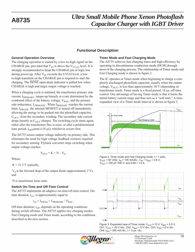
Timer Mode and Fast Charging ModeThe A8735 achieves fast charging times and high efficiency by operating in discontinuous conduction mode (DCM) through most of the charging process. The relationship of Timer mode and Fast Charging mode is shown in figure 2.
The IC operates in Timer mode when beginning to charge a com-pletely discharged photoflash capacitor, usually when the output voltage, VOUT , is less than approximately 30 V (depending on transformer used). Timer mode is a fixed period, 18 たs, off-time control. One advantage of having Timer mode is that it limits the initial battery current surge and thus acts as a “soft-start.” A time-expanded view of a Timer mode interval is shown in figure 3.
Functional Description
Figure 2. Timer mode and Fast Charging mode: t = 1 s/div; VOUT = 50 V/div; IIN = 100 mA/div., VIN = VBAT = 3.6 V; COUT = 100 たF / 330 V; and ILIM = 1.0 A.
VOUT
IIN
Figure 3. Expanded view of Timer mode: VOUT ≤ 10 V, VBAT = 5.5 V, Ch1: VOUT = 20 V / div., Ch2: VBAT = 5 V / div., Ch3: VSW = 5 V / div., Ch4: ISW = 500 mA / div., t = 5 たs / div.
C2,C3
C4
C1
VOUT
VSW
ISW
VBAT
Ultra Small Mobile Phone Xenon Photoflash Capacitor Charger with IGBT Driver
11Allegro MicroSystems, Inc.115 Northeast CutoffWorcester, Massachusetts 01615-0036 U.S.A.1.508.853.5000; www.allegromicro.com
A8735
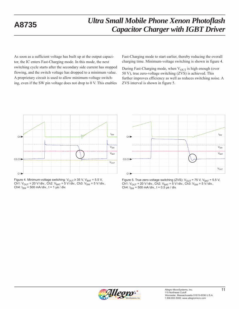
As soon as a sufficient voltage has built up at the output capaci-
tor, the IC enters Fast-Charging mode. In this mode, the next
switching cycle starts after the secondary side current has stopped
flowing, and the switch voltage has dropped to a minimum value.
A proprietary circuit is used to allow minimum-voltage switch-
ing, even if the SW pin voltage does not drop to 0 V. This enables
Fast-Charging mode to start earlier, thereby reducing the overall
charging time. Minimum-voltage switching is shown in figure 4.
During Fast-Charging mode, when VOUT is high enough (over
50 V), true zero-voltage switching (ZVS) is achieved. This
further improves efficiency as well as reduces switching noise. A
ZVS interval is shown in figure 5.
Figure 4. Minimum-voltage switching: VOUT ≥ 35 V, VBAT = 5.5 V, Ch1: VOUT = 20 V / div., Ch2: VBAT = 5 V / div., Ch3: VSW = 5 V / div., Ch4: ISW = 500 mA / div., t = 1 たs / div.
Figure 5. True zero-voltage switching (ZVS): VOUT = 75 V, VBAT = 5.5 V, Ch1: VOUT = 20 V / div., Ch2: VBAT = 5 V / div., Ch3: VSW = 5 V / div., Ch4: ISW = 500 mA / div., t = 0.5 たs / div.
C2,C3
C4
C1
VOUT
VSW
ISW
VBAT
C2,C3
C4
C1
VOUT
VSW
ISW
VBAT
Ultra Small Mobile Phone Xenon Photoflash Capacitor Charger with IGBT Driver
12Allegro MicroSystems, Inc.115 Northeast CutoffWorcester, Massachusetts 01615-0036 U.S.A.1.508.853.5000; www.allegromicro.com
A8735
Applications Information
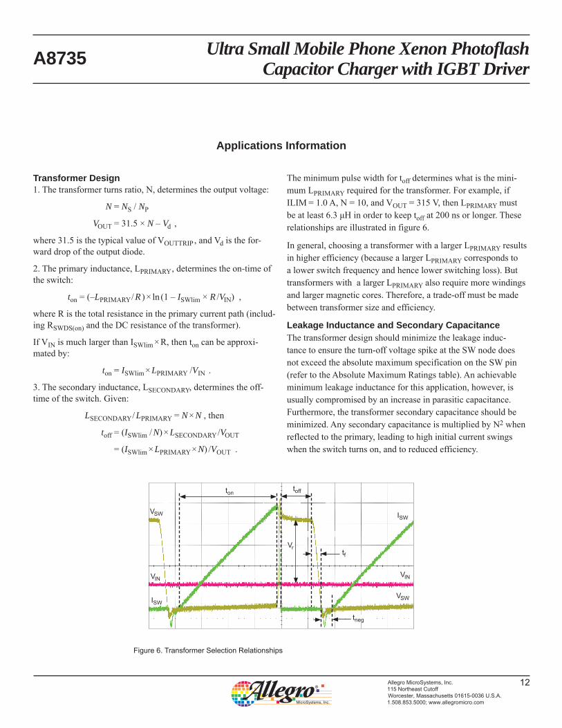
Transformer Design1. The transformer turns ratio, N, determines the output voltage:
N = NS / NP
VOUT = 31.5 × N – Vd ,
where 31.5 is the typical value of VOUTTRIP , and Vd is the for-
ward drop of the output diode.
2. The primary inductance, LPRIMARY , determines the on-time of
the switch:
ton = (–LPRIMARY / R ) × ln (1 – ISWlim × R /VIN) ,
where R is the total resistance in the primary current path (includ-
ing RSWDS(on) and the DC resistance of the transformer).
If VIN is much larger than ISWlim × R, then ton can be approxi-
mated by:
ton = ISWlim × LPRIMARY /VIN .
3. The secondary inductance, LSECONDARY, determines the off-
time of the switch. Given:
LSECONDARY / LPRIMARY = N × N , then
toff = (ISWlim / N) × LSECONDARY /VOUT
= (ISWlim × LPRIMARY × N) /VOUT .
The minimum pulse width for toff determines what is the mini-
mum LPRIMARY required for the transformer. For example, if
ILIM = 1.0 A, N = 10, and VOUT = 315 V, then LPRIMARY must
be at least 6.3 たH in order to keep toff at 200 ns or longer. These
relationships are illustrated in figure 6.
In general, choosing a transformer with a larger LPRIMARY results
in higher efficiency (because a larger LPRIMARY corresponds to
a lower switch frequency and hence lower switching loss). But
transformers with a larger LPRIMARY also require more windings
and larger magnetic cores. Therefore, a trade-off must be made
between transformer size and efficiency.
Leakage Inductance and Secondary CapacitanceThe transformer design should minimize the leakage induc-
tance to ensure the turn-off voltage spike at the SW node does
not exceed the absolute maximum specification on the SW pin
(refer to the Absolute Maximum Ratings table). An achievable
minimum leakage inductance for this application, however, is
usually compromised by an increase in parasitic capacitance.
Furthermore, the transformer secondary capacitance should be
minimized. Any secondary capacitance is multiplied by N2 when
reflected to the primary, leading to high initial current swings
when the switch turns on, and to reduced efficiency.
Figure 6. Transformer Selection Relationships
VSW
VSW
VINVIN
ISW
ISW
tontoff
Vrtf
tneg
Ultra Small Mobile Phone Xenon Photoflash Capacitor Charger with IGBT Driver
13Allegro MicroSystems, Inc.115 Northeast CutoffWorcester, Massachusetts 01615-0036 U.S.A.1.508.853.5000; www.allegromicro.com
A8735
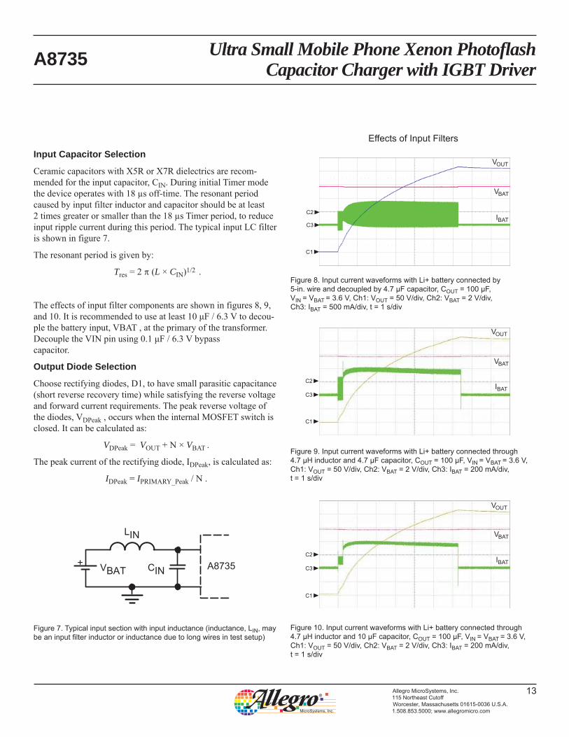
Input Capacitor Selection
Ceramic capacitors with X5R or X7R dielectrics are recom-mended for the input capacitor, CIN. During initial Timer mode the device operates with 18 μs off-time. The resonant period caused by input filter inductor and capacitor should be at least 2 times greater or smaller than the 18 μs Timer period, to reduce input ripple current during this period. The typical input LC filter is shown in figure 7.
The resonant period is given by:
Tres = 2 ° (L × CIN)1/2 .
The effects of input filter components are shown in figures 8, 9, and 10. It is recommended to use at least 10 たF / 6.3 V to decou-ple the battery input, VBAT , at the primary of the transformer. Decouple the VIN pin using 0.1 たF / 6.3 V bypass capacitor.
Output Diode Selection
Choose rectifying diodes, D1, to have small parasitic capacitance (short reverse recovery time) while satisfying the reverse voltage and forward current requirements. The peak reverse voltage of the diodes, VDPeak , occurs when the internal MOSFET switch is closed. It can be calculated as:
VDPeak = VOUT + N × VBAT .
The peak current of the rectifying diode, IDPeak, is calculated as:
IDPeak = IPRIMARY_Peak / N .
+ CIN A8735VBAT
LIN
Figure 7. Typical input section with input inductance (inductance, LIN, may be an input filter inductor or inductance due to long wires in test setup)
Effects of Input Filters
Figure 9. Input current waveforms with Li+ battery connected through 4.7 たH inductor and 4.7 たF capacitor, COUT = 100 μF, VIN = VBAT = 3.6 V, Ch1: VOUT = 50 V/div, Ch2: VBAT = 2 V/div, Ch3: IBAT = 200 mA/div, t = 1 s/div
Figure 10. Input current waveforms with Li+ battery connected through 4.7 たH inductor and 10 たF capacitor, COUT = 100 μF, VIN = VBAT = 3.6 V, Ch1: VOUT = 50 V/div, Ch2: VBAT = 2 V/div, Ch3: IBAT = 200 mA/div, t = 1 s/div
VOUT
VBAT
IBAT
C2
C3
C1
VOUT
VBAT
IBAT
C2
C3
C1
Figure 8. Input current waveforms with Li+ battery connected by 5-in. wire and decoupled by 4.7 たF capacitor, COUT = 100 μF, VIN = VBAT = 3.6 V, Ch1: VOUT = 50 V/div, Ch2: VBAT = 2 V/div, Ch3: IBAT = 500 mA/div, t = 1 s/div
VOUT
VBAT
IBATC3
C2
C1
Ultra Small Mobile Phone Xenon Photoflash Capacitor Charger with IGBT Driver
14Allegro MicroSystems, Inc.115 Northeast CutoffWorcester, Massachusetts 01615-0036 U.S.A.1.508.853.5000; www.allegromicro.com
A8735
Recommended Components
Component Rating Part Number Source
C1, Input Capacitor 10 たF, ±10%, 6.3 V, X5R ceramic capacitor (0805)
JMK212BJ106K Taiyo Yuden
C2 0.1 μF, 6.3 V X5R ceramic capacitor
COUT, Photoflash Capacitor
100 たF / 330 V EPH-31ELL101B131S Chemi-Con
D1, Output Diode 2 x 250 V, 225 mA, 5 pF BAV23S Philips Semiconductor, Fairchild Semiconductor
T1, Transformer
LPRIMARY = 12.8 μH, N= 10.25, 6.5 × 8 × 4 mm
T-16-024A Tokyo Coil Electric
LPRIMARY = 7.8 μH, N= 9.9, 4.6 × 4.6 × 2.4 mm
MTF-S2 Union
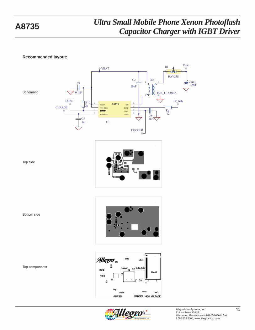
Layout GuidelinesKey to a good layout for the photoflash capacitor charger circuit
is to keep the parasitics minimized on the power switch loop
(transformer primary side) and the rectifier loop (secondary side).
Use short, thick traces for connections to the transformer primary
and SW pin. It is important that the D ¯ O N E signal trace and other
signal traces be routed away from the transformer and other
switching traces, in order to minimize noise pickup. In addition,
high voltage isolation rules must be followed carefully to avoid
breakdown failure of the circuit board.
Avoid placing any ground plane area underneath the transformer
secondary and diode, to minimize parasitic capacitance.
For low threshold logic (<1.2 V) add 1 nF capacitors across the
CHARGE and TRIGGER pins to GND to avoid malfunction due
to noise.
Connect the EE package PAD to the ground pad for better ther-
mal performance. Use ground planes on the top and bottom layers
below the IC and connect them through multiple thermal vias.
Refer to the figures on page 18 for recommended layout.
Ultra Small Mobile Phone Xenon Photoflash Capacitor Charger with IGBT Driver
15Allegro MicroSystems, Inc.115 Northeast CutoffWorcester, Massachusetts 01615-0036 U.S.A.1.508.853.5000; www.allegromicro.com
A8735
Recommended layout:
Schematic
Top side
Bottom side
Top components
0.1uF
C410uF
C2
VBAT
TRIGGER
CHARGE
DONE
Cout1100uF
3
4
1
2X2
TCE_T-16-024A
12Rg
SW5
CHARGE8
GATE3
DONE1
VIN_DRV7
TRIG2
GND4
VBAT6
U1
Vout
TP_Gate
2kR10
3
1 2
D1
BAV23S
1nF
C5 1nFC6
A8735
Ultra Small Mobile Phone Xenon Photoflash Capacitor Charger with IGBT Driver
16Allegro MicroSystems, Inc.115 Northeast CutoffWorcester, Massachusetts 01615-0036 U.S.A.1.508.853.5000; www.allegromicro.com
A8735
Copyright ©2010, Allegro MicroSystems, Inc.The products described here are manufactured under one or more U.S. patents or U.S. patents pending. Allegro MicroSystems, Inc. reserves the right to make, from time to time, such de par tures from the detail spec i fi ca tions as may be required to per-
mit improvements in the per for mance, reliability, or manufacturability of its products. Before placing an order, the user is cautioned to verify that the information being relied upon is current.
Allegro’s products are not to be used in life support devices or systems, if a failure of an Allegro product can reasonably be expected to cause the failure of that life support device or system, or to affect the safety or effectiveness of that device or system.
The in for ma tion in clud ed herein is believed to be ac cu rate and reliable. How ev er, Allegro MicroSystems, Inc. assumes no re spon si bil i ty for its use; nor for any in fringe ment of patents or other rights of third parties which may result from its use.
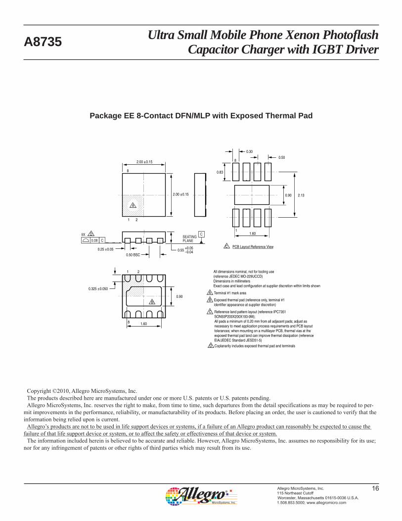
Package EE 8-Contact DFN/MLP with Exposed Thermal Pad
1.60
8
8
21
21
A
A Terminal #1 mark area
B Exposed thermal pad (reference only, terminal #1
identifier appearance at supplier discretion)
All dimensions nominal, not for tooling use
(reference JEDEC MO-229UCCD)
Dimensions in millimeters
Exact case and lead configuration at supplier discretion within limits shown
C Reference land pattern layout (reference IPC7351
SON50P200X200X100-9M);
All pads a minimum of 0.20 mm from all adjacent pads; adjust as
necessary to meet application process requirements and PCB layout
tolerances; when mounting on a multilayer PCB, thermal vias at the
exposed thermal pad land can improve thermal dissipation (reference
EIA/JEDEC Standard JESD51-5)
B
PCB Layout Reference View
0.90
1.60
0.30
1
80.50
0.83
2.13
C
0.90
0.55+0.05–0.04
2.00 ±0.15
2.00 ±0.15
0.25 ±0.05
0.325 ±0.050
0.50 BSC
C0.08
D
D
Coplanarity includes exposed thermal pad and terminals
CSEATINGPLANE
9X


![[New Symmetry Issue] Xenon, Xenon Everywhere; A Measurement to Watch](https://static.cupdf.com/doc/110x72/563db844550346aa9a9221ed/new-symmetry-issue-xenon-xenon-everywhere-a-measurement-to-watch.jpg)

