Types of Materials• Metals:
– Strong, ductile– high thermal & electrical conductivity– opaque
• Polymers/plastics: Covalent bonding sharing of e’s– Soft, ductile, low strength, low density– thermal & electrical insulators– Optically translucent or transparent.
• Ceramics: ionic bonding (refractory) – compounds of metallic & non-metallic elements (oxides, carbides, nitrides, sulfides)– Brittle, glassy, elastic– non-conducting (insulators)
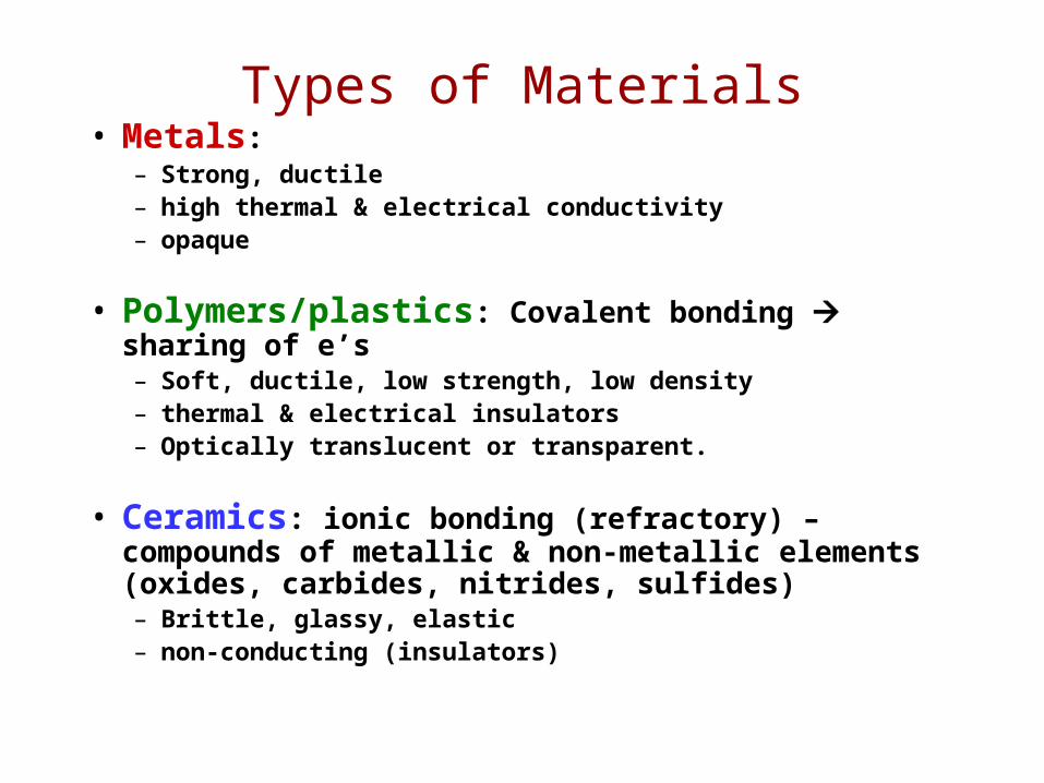
Material Density

Material Stiffness
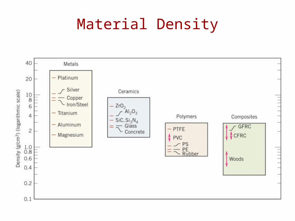
Material Resistance to Fracture

Material Electrical Conductivity

The Materials Selection Process
ApplicationsFunctions
Properties
Materials
Processes
EnvironmentLoad
StructureShape
CompositionMechanical
ElectricalThermal
OpticalEtc.

ex: hardness vs structure of steel • Properties depend on structure
Steel with 0.4 wt% C d) Martensite
c) Martensite (tempered at 371 C)
b) Fine pearlite
a) Spheroidite
ex: structure vs cooling rate of steel • Processing can change structure
Structure, Processing, & PropertiesH
ardn
ess
(BH
N)
Cooling Rate (ºC/s)
100
200
300
400
500
600
0.01 0.1 1 10 100 1000
(d)
30 m(c)
4 m
(b)
30 m
(a)
30 m
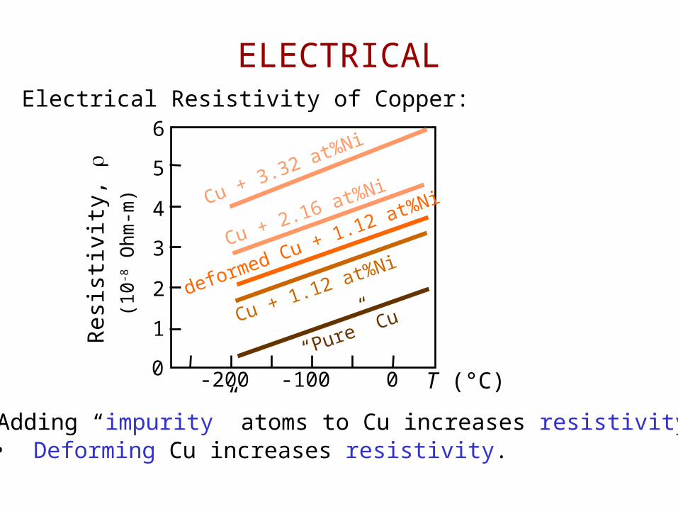
ELECTRICAL• Electrical Resistivity of Copper:
• Adding “impurity” atoms to Cu increases resistivity.• Deforming Cu increases resistivity.
T (°C)-200 -100 0
Cu + 3.32 at%Ni
Cu + 2.16 at%Ni
deformed Cu + 1.12 at%Ni
1
2
3
4
5
6
Res
istiv
ity,
(10-8
Oh
m-m
)
0
Cu + 1.12 at%Ni
“Pure” Cu
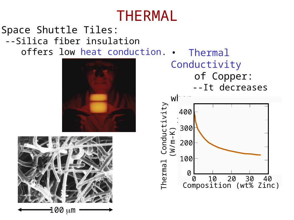
THERMAL• Space Shuttle Tiles: --Silica fiber insulation offers low heat conduction. • Thermal Conductivity
of Copper: --It decreases when you add zinc!
Composition (wt% Zinc)
The
rmal
Con
duct
ivity
(W
/m-K
)
400
300
200
100
00 10 20 30 40
100 m

MAGNETIC
• Magnetic Permeability vs. Composition: --Adding 3 atomic % Si makes Fe a better recording medium!
• Magnetic Storage: --Recording medium is magnetized by recording head.
Magnetic Field
Ma
gn
etiz
atio
n Fe+3%Si
Fe
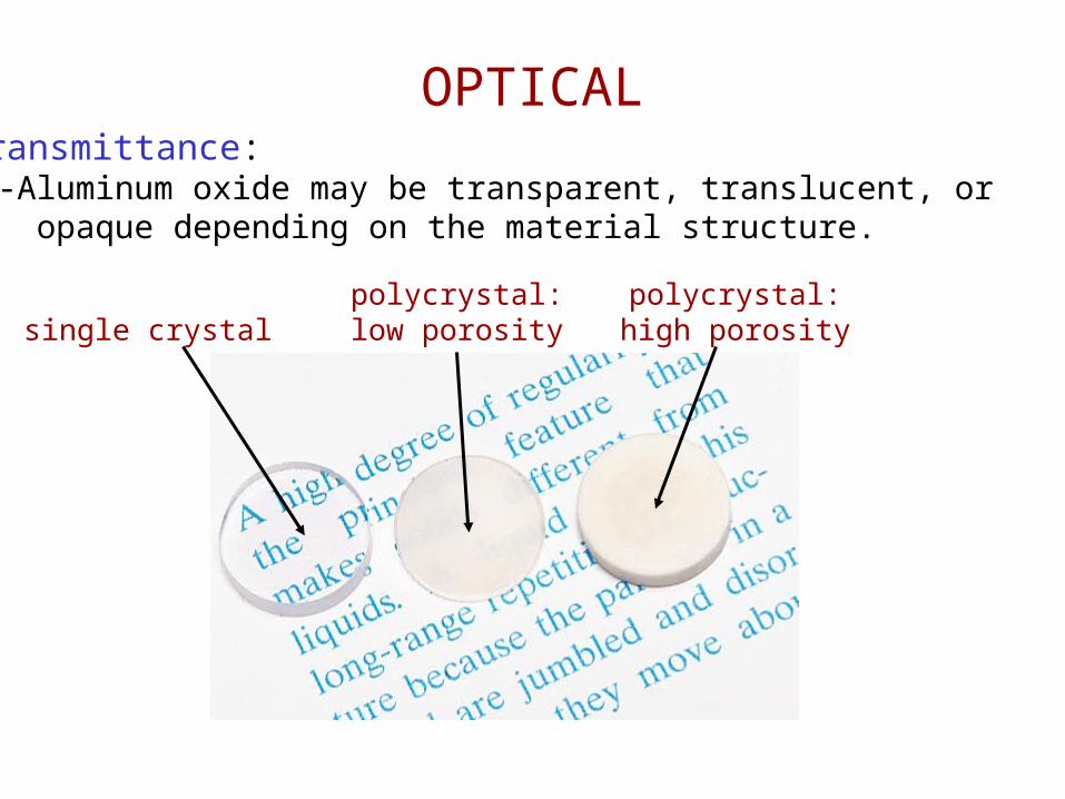
• Transmittance: --Aluminum oxide may be transparent, translucent, or opaque depending on the material structure.
single crystalpolycrystal:low porosity
polycrystal:high porosity
OPTICAL
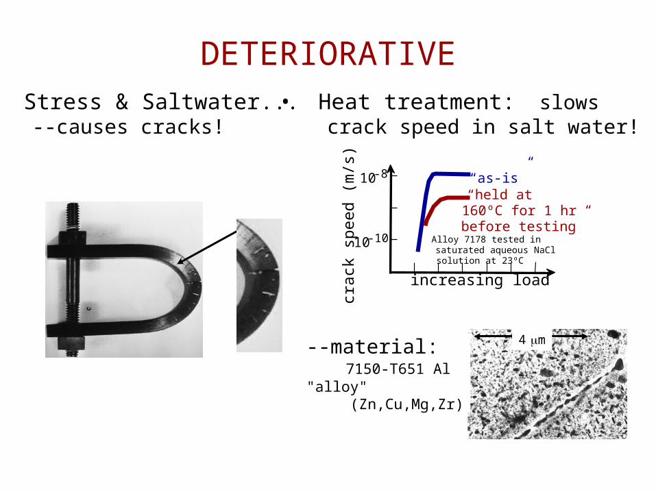
DETERIORATIVE• Stress & Saltwater... --causes cracks!
4 m--material: 7150-T651 Al "alloy" (Zn,Cu,Mg,Zr)
• Heat treatment: slows crack speed in salt water!
“held at 160ºC for 1 hr before testing”
increasing loadcrac
k sp
eed
(m
/s)
“as-is”
10-10
10-8
Alloy 7178 tested in saturated aqueous NaCl solution at 23ºC

• Bond length, r
• Bond energy, Eo
• Melting Temperature, Tm
Tm is larger if Eo is larger.
Properties From Bonding: Tm
r o r
Energyr
larger Tm
smaller Tm
Eo =
“bond energy”
Energy
r o r
unstretched length
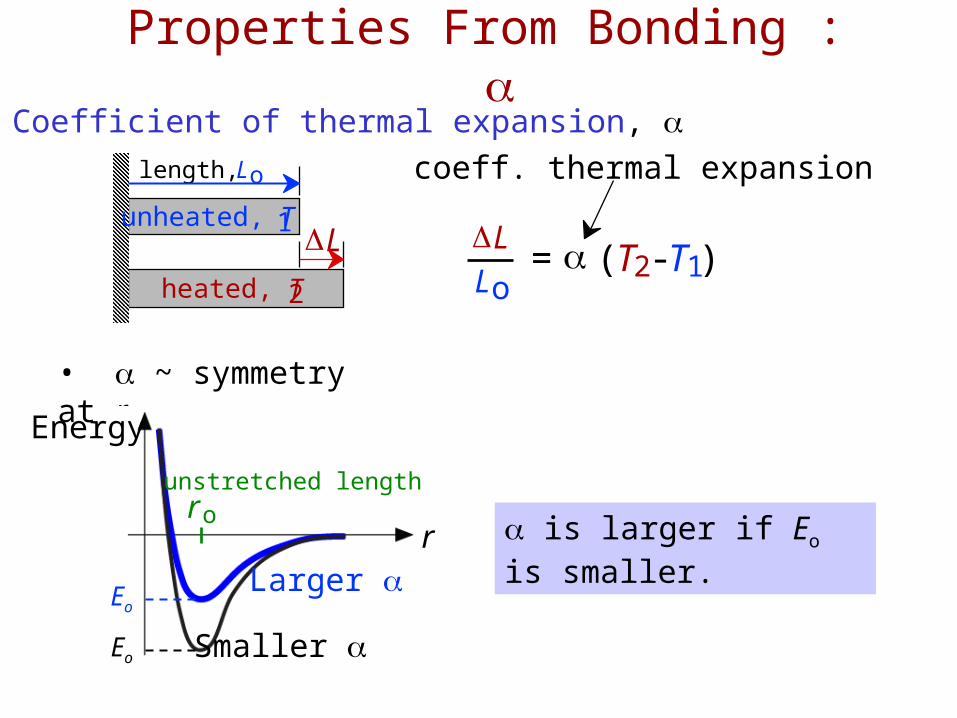
• Coefficient of thermal expansion,
• ~ symmetry at ro
is larger if Eo is smaller.
Properties From Bonding :
= (T2 -T1)LLo
coeff. thermal expansion
L
length, Lo
unheated, T1
heated, T2
r or
Smaller
Larger
Energy
unstretched length
Eo
Eo

Ceramics(Ionic & covalent bonding):
Metals(Metallic bonding):
Polymers(Covalent & Secondary):
Large bond energylarge Tmlarge Esmall
Variable bond energymoderate Tmmoderate Emoderate
Secondary bonding dominates small Tm small E large
Summary: Primary Bonds
secondary bonding
Brief of Metal

The Periodic Table
• Columns: Similar Valence Structure
O
Se
Te
Po At
I
He
Ne
Ar
Kr
Xe
Rn
F
ClS
Li Be
H
Na Mg
BaCs
RaFr
CaK Sc
SrRb Y
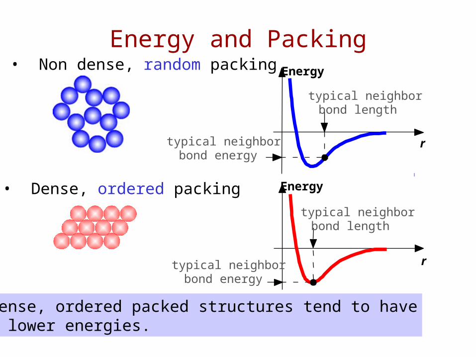
• Non dense, random packing
• Dense, ordered packing
Dense, ordered packed structures tend to have lower energies.
Energy and PackingEnergy
r
typical neighbor bond length
typical neighbor bond energy
Energy
r
typical neighbor bond length
typical neighbor bond energy

• atoms pack in periodic, 3D arraysCrystalline materials...
-metals-many ceramics-some polymers
• atoms have no periodic packingNoncrystalline materials...
-complex structures-rapid cooling
crystalline SiO2
noncrystalline SiO2"Amorphous" = Noncrystalline
Materials and Packing
Si Oxygen
• typical of:
• occurs for:
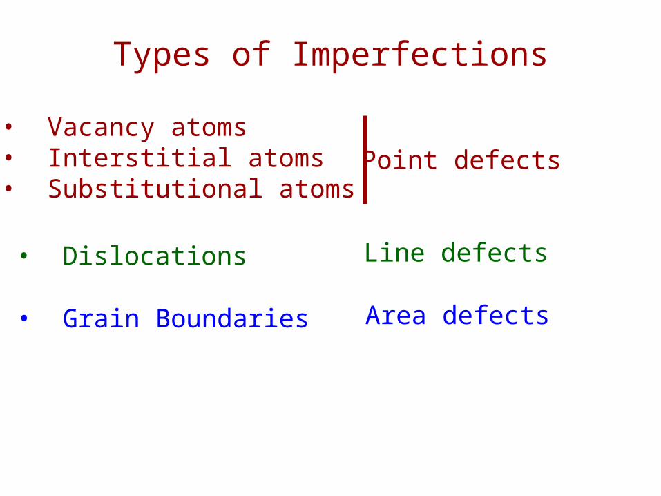
• Vacancy atoms• Interstitial atoms• Substitutional atoms
Point defects
Types of Imperfections
• Dislocations Line defects
• Grain Boundaries Area defects
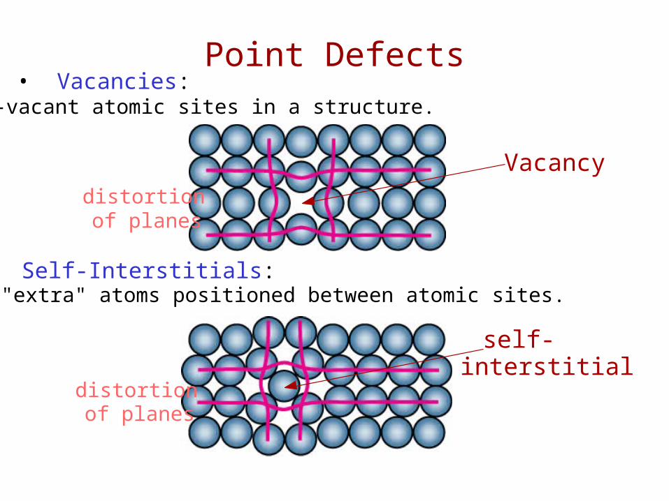
• Vacancies:-vacant atomic sites in a structure.
• Self-Interstitials:-"extra" atoms positioned between atomic sites.
Point Defects
Vacancydistortion of planes
self-interstitial
distortion of planes

Two outcomes if impurity (B) added to host (A):• Solid solution of B in A (i.e., random dist. of point defects)
• Solid solution of B in A plus a new phase (usually for a larger amount of B)
OR
Substitutional solid soln.(e.g., Cu in Ni)
Interstitial solid soln.(e.g., C in Fe)
Second phase particle--different composition--often different structure.
Point Defects in Alloys

• are line defects,• slip between crystal planes result when dislocations move,• produce permanent (plastic) deformation.
Dislocations:
Schematic of Zinc (HCP):• before deformation • after tensile elongation
slip steps
Line Defects
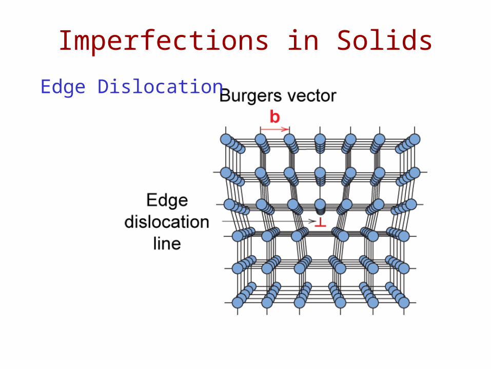
Imperfections in Solids
Edge Dislocation
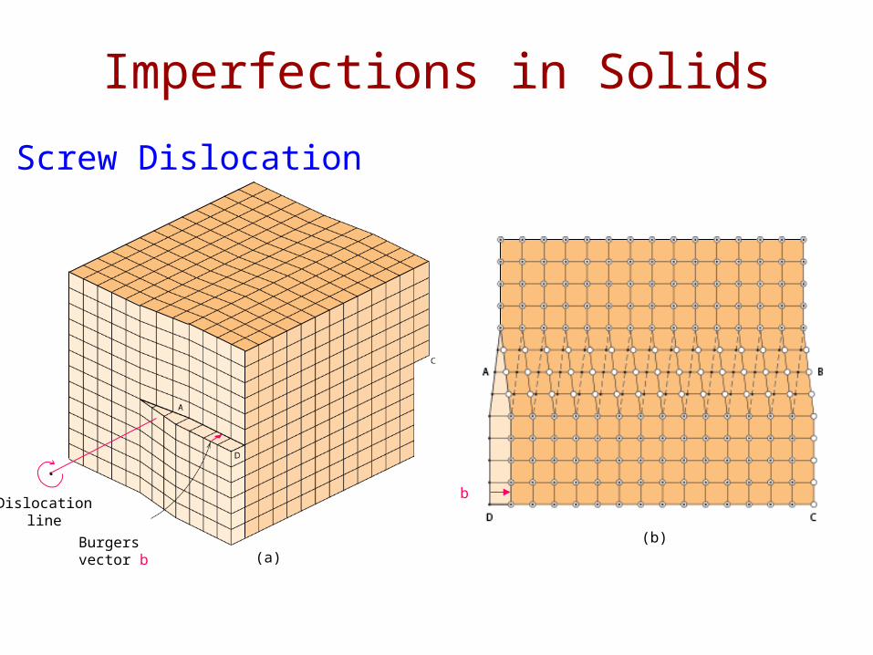
Imperfections in Solids
Screw Dislocation
Burgers vector b
Dislocationline
b
(a)(b)
Screw Dislocation

Edge, Screw, and Mixed Dislocations
Edge
Screw
Mixed
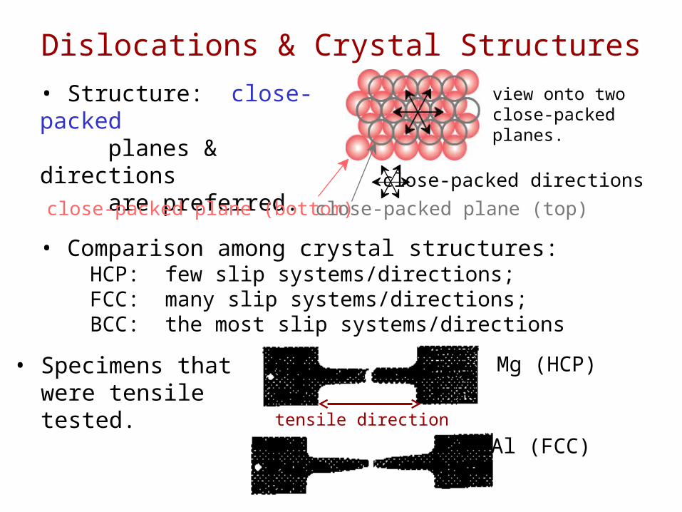
Dislocations & Crystal Structures
• Structure: close-packed planes & directions are preferred.
view onto twoclose-packedplanes.
close-packed plane (bottom) close-packed plane (top)
close-packed directions
• Comparison among crystal structures: HCP: few slip systems/directions; FCC: many slip systems/directions; BCC: the most slip systems/directions
• Specimens that were tensile tested.
Mg (HCP)
Al (FCC)tensile direction
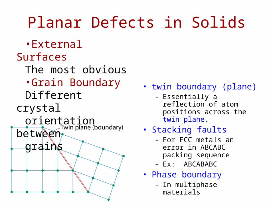
Planar Defects in Solids
• twin boundary (plane) – Essentially a reflection of
atom positions across the twin plane.
• Stacking faults– For FCC metals an error in
ABCABC packing sequence
– Ex: ABCABABC
• Phase boundary– In multiphase materials
•External SurfacesThe most obvious•Grain BoundaryDifferent crystal orientation between grains

Polycrystalline Materials
Grain Boundaries• regions between crystals• transition from lattice of one
region to that of the other• slightly disordered• low density in grain
boundaries– high mobility– high diffusivity– high chemical reactivity