
To learn more about ON Semiconductor, please visit our website at www.onsemi.com
Is Now Part of
ON Semiconductor and the ON Semiconductor logo are trademarks of Semiconductor Components Industries, LLC dba ON Semiconductor or its subsidiaries in the United States and/or other countries. ON Semiconductor owns the rights to a number of patents, trademarks, copyrights, trade secrets, and other intellectual property. A listing of ON Semiconductor’s product/patent coverage may be accessed at www.onsemi.com/site/pdf/Patent-Marking.pdf. ON Semiconductor reserves the right to make changes without further notice to any products herein. ON Semiconductor makes no warranty, representation or guarantee regarding the suitability of its products for any particular purpose, nor does ON Semiconductor assume any liability arising out of the application or use of any product or circuit, and specifically disclaims any and all liability, including without limitation special, consequential or incidental damages. Buyer is responsible for its products and applications using ON Semiconductor products, including compliance with all laws, regulations and safety requirements or standards, regardless of any support or applications information provided by ON Semiconductor. “Typical” parameters which may be provided in ON Semiconductor data sheets and/or specifications can and do vary in different applications and actual performance may vary over time. All operating parameters, including “Typicals” must be validated for each customer application by customer’s technical experts. ON Semiconductor does not convey any license under its patent rights nor the rights of others. ON Semiconductor products are not designed, intended, or authorized for use as a critical component in life support systems or any FDA Class 3 medical devices or medical devices with a same or similar classification in a foreign jurisdiction or any devices intended for implantation in the human body. Should Buyer purchase or use ON Semiconductor products for any such unintended or unauthorized application, Buyer shall indemnify and hold ON Semiconductor and its officers, employees, subsidiaries, affiliates, and distributors harmless against all claims, costs, damages, and expenses, and reasonable attorney fees arising out of, directly or indirectly, any claim of personal injury or death associated with such unintended or unauthorized use, even if such claim alleges that ON Semiconductor was negligent regarding the design or manufacture of the part. ON Semiconductor is an Equal Opportunity/Affirmative Action Employer. This literature is subject to all applicable copyright laws and is not for resale in any manner.
Application Note AN4149Design Guidelines for Quasi-Resonant Converters Using KA5Q-series Fairchild Power Switch (FPSTM)
www.fairchildsemi.com
©2005 Fairchild Semiconductor Corporation
AbstractIn general, a Quasi-Resonant Converter (QRC) shows lowerEMI and higher power conversion efficiency compared tothe conventional hard switched converter with a fixedswitching frequency. Therefore, it is well suited for color TVapplications that are noise sensitive. This application notepresents practical design considerations of Quasi-Resonant
Converters for color TV applications employing KA5Q-series FPSTM (Fairchild Power Switch). It includesdesigning the transformer, output filter and sync network,selecting the components and closing the feedback loop. Thestep-by-step design procedure described in this applicationnote will help engineers design quasi-resonant convertereasily.
Rev. 1.0.0
1. IntroductionThe KA5Q-series FPSTM (Fairchild Power Switch) is anintegrated Pulse Width Modulation (PWM) controller and aSense FET specifically designed for quasi-resonant off-lineSwitch Mode Power Supplies (SMPS) with minimal externalcomponents. Compared with a discrete MOSFET and PWMcontroller solution, it can reduce total cost, component count,size and weight while simultaneously increasing efficiency,
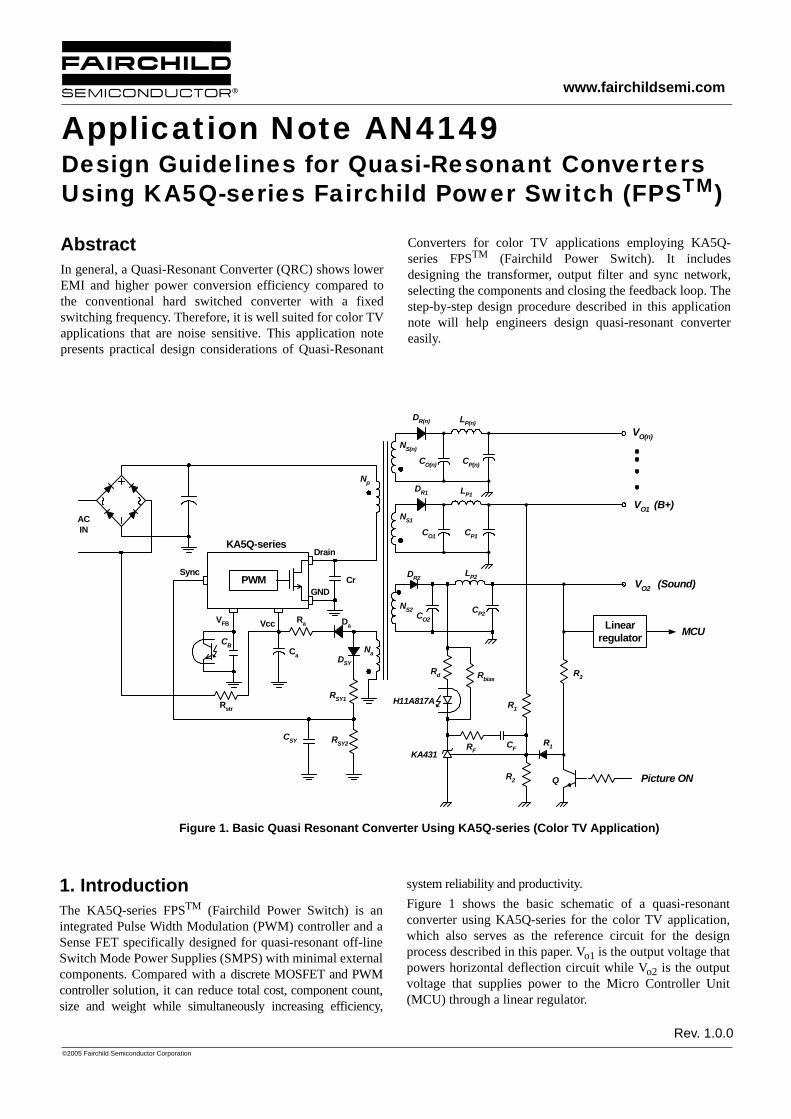
system reliability and productivity.Figure 1 shows the basic schematic of a quasi-resonantconverter using KA5Q-series for the color TV application,which also serves as the reference circuit for the designprocess described in this paper. Vo1 is the output voltage thatpowers horizontal deflection circuit while Vo2 is the outputvoltage that supplies power to the Micro Controller Unit(MCU) through a linear regulator.
Figure 1. Basic Quasi Resonant Converter Using KA5Q-series (Color TV Application)
Vcc
GND
Drain
SyncPWM
VFB
ACIN
KA5Q-series
NS2
DR2
CO2
KA431
H11A817A
Rd Rbias
R1
R2
RFCF
LP2
CP2
VO1 (B+)
VO2 (Sound)
DR1 LP1
CO1 CP1
Linearregulator MCU
Picture ON
R3
R1
Q
Na
Np
NS1
Cr
DSY
RSY1
RSY2CSY
CB
Ra
Ca
DR(n) LP(n)
CO(n) CP(n)
NS(n)
VO(n)
Da
Rstr

AN4149 APPLICATION NOTE
2
©2005 Fairchild Semiconductor Corporation
2. Step-by-step Design Procedure
Figure 2. Flow Chart of Design Procedure
In this section, a design procedure is presented using theschematic of Figure 1 as a reference. Figure 2 illustrates thedesign flow chart. The detailed design procedures are asfollows:
[STEP-1] Define the system specifications
- Line voltage range (Vlinemin and Vline
max). - Line frequency (fL). - Maximum output power (Po). - Estimated efficiency (Eff) : The power conversionefficiency must be estimated to calculate the maximum inputpower. If no reference data is available, set Eff = 0.7~0.75 forlow voltage output applications and Eff = 0.8~0.85 for highvoltage output applications. In the case of Color TVapplications, the typical efficiency is 80~83%.
With the estimated efficiency, the maximum input power isgiven by
For multiple output SMPS, the load occupying factor foreach output is defined as
where Po(n) is the maximum output power for the n-thoutput. For single output SMPS, KL(1)=1. It is assumed thatVo1 is the reference output that is regulated by the feedbackcontrol in normal operation.
[STEP-2] Determine DC link capacitor (CDC) and the DC link voltage range.
It is typical to select the DC link capacitor as 2-3uF per wattof input power for universal input range (85-265Vrms) and1uF per watt of input power for European input range (195V-265Vrms). With the DC link capacitor chosen, the minimumDC link voltage is obtained as
where CDC is the DC link capacitor and Dch is the duty cycleratio for CDC to be charged as defined in Figure 3, which istypically about 0.2. Pin, Vline
min and fL are specified inSTEP-1.
The maximum DC link voltage is given as
where Vlinemax is specified in STEP-1.
1. Define the system specifications(Vline
min, Vlinemax, fL , Po , Eff )
2. Determine DC link capacitor (CDC) and DC link voltage range
3. Determine the reflected output voltage(VRO)
6. Determine the proper core and theminimum primary turns (Np
min)
7. Determine the number of turns for eachoutput
5. Choose proper FPS considering inputpower and Ids
peak
4. Determine the transformer primary sideinductance (Lm)
Is the winding windowarea (Aw) enough ?
Y
N
Is it possible to change the core ?Y
N
8. Determine the startup resistor
9. Determine the wire diameter for eachwinding
13. Design the voltage drop circuit for burstoperation
Design finished
14. Design the feedback control circuit
12. Design the synchronization network
11. Determine the output capacitors
10. Choose the secondary side rectifier diodes
PinPoEff-------= (1)
KL n( )Po n( )
Po-------------= (2)
VDCmin 2 Vline
min( )⋅2 Pin 1 Dch–( )⋅
CDC fL⋅------------------------------------–= (3)
VDCmax 2Vline
max= (4)
APPLICATION NOTE AN4149
3
©2005 Fairchild Semiconductor Corporation
Figure 3. DC Link Voltage Waveform
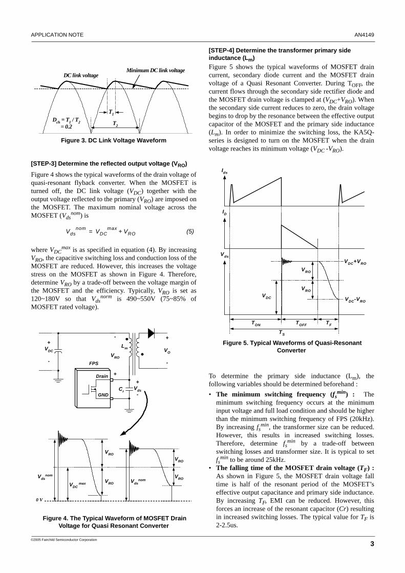
[STEP-3] Determine the reflected output voltage (VRO)
Figure 4 shows the typical waveforms of the drain voltage ofquasi-resonant flyback converter. When the MOSFET isturned off, the DC link voltage (VDC) together with theoutput voltage reflected to the primary (VRO) are imposed onthe MOSFET. The maximum nominal voltage across theMOSFET (Vds
nom) is
where VDCmax is as specified in equation (4). By increasing
VRO, the capacitive switching loss and conduction loss of theMOSFET are reduced. However, this increases the voltagestress on the MOSFET as shown in Figure 4. Therefore,determine VRO by a trade-off between the voltage margin ofthe MOSFET and the efficiency. Typically, VRO is set as120~180V so that Vds
norm is 490~550V (75~85% ofMOSFET rated voltage).
Figure 4. The Typical Waveform of MOSFET Drain Voltage for Quasi Resonant Converter
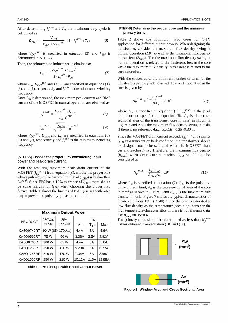
[STEP-4] Determine the transformer primary side inductance (Lm)Figure 5 shows the typical waveforms of MOSFET draincurrent, secondary diode current and the MOSFET drainvoltage of a Quasi Resonant Converter. During TOFF, thecurrent flows through the secondary side rectifier diode andthe MOSFET drain voltage is clamped at (VDC+VRO). Whenthe secondary side current reduces to zero, the drain voltagebegins to drop by the resonance between the effective outputcapacitor of the MOSFET and the primary side inductance(Lm). In order to minimize the switching loss, the KA5Q-series is designed to turn on the MOSFET when the drainvoltage reaches its minimum voltage (VDC -VRO).
Figure 5. Typical Waveforms of Quasi-Resonant Converter
To determine the primary side inductance (Lm), thefollowing variables should be determined beforehand :• The minimum switching frequency (fs
min) : Theminimum switching frequency occurs at the minimuminput voltage and full load condition and should be higherthan the minimum switching frequency of FPS (20kHz).By increasing fs
min, the transformer size can be reduced.However, this results in increased switching losses.Therefore, determine fs
min by a trade-off betweenswitching losses and transformer size. It is typical to setfs
min to be around 25kHz. • The falling time of the MOSFET drain voltage (TF) :
As shown in Figure 5, the MOSFET drain voltage falltime is half of the resonant period of the MOSFET’seffective output capacitance and primary side inductance.By increasing TF, EMI can be reduced. However, thisforces an increase of the resonant capacitor (Cr) resultingin increased switching losses. The typical value for TF is2-2.5us.
DC link voltageMinimum DC link voltage
T1
T2Dch = T1 / T2
= 0.2
Vdsnom VDC
max VRO+= (5)
-
VRO
+
+VDC
-
Drain
GND
FPS
+Vds
-
0 V
VDC max
VRO
VRO
Vdsnom
Lm
Cr
+
VO
-
VRO
VROVdsnom
VDC
VRO
VRO
Vds
Ids
TFTOFFTON
TS
ID
VDC+VRO
VDC-VRO
AN4149 APPLICATION NOTE
4
©2005 Fairchild Semiconductor Corporation
After determining fsmin and TF, the maximum duty cycle iscalculated as
where VDCmin is specified in equation (3) and VRO is
determined in STEP-3.Then, the primary side inductance is obtained as
where Pin, VDCmin and Dmax are specified in equations (1),
(3), and (6), respectively and fsmin is the minimum switchingfrequency.Once Lm is determined, the maximum peak current and RMScurrent of the MOSFET in normal operation are obtained as
where VDCmin, Dmax and Lm are specified in equations (3),
(6) and (7), respectively and fsmin is the minimum switching
frequency.
[STEP-5] Choose the proper FPS considering input power and peak drain current.
With the resulting maximum peak drain current of theMOSFET (Ids
peak) from equation (8), choose the proper FPSwhose pulse-by-pulse current limit level (ILIM) is higher thanIds
peak. Since FPS has ± 12% tolerance of ILIM, there shouldbe some margin for ILIM when choosing the proper FPSdevice. Table 1 shows the lineups of KA5Q-series with ratedoutput power and pulse-by-pulse current limit.
Table 1. FPS Lineups with Rated Output Power
[STEP-6] Determine the proper core and the minimum primary turns.
Table 2 shows the commonly used cores for C-TVapplication for different output powers. When designing thetransformer, consider the maximum flux density swing innormal operation (∆B) as well as the maximum flux densityin transient (Bmax). The the maximum flux density swing innormal operation is related to the hysteresis loss in the corewhile the maximum flux density in transient is related to thecore saturation.
With the chosen core, the minimum number of turns for thetransformer primary side to avoid the over temperature in thecore is given by
where Lm is specified in equation (7), Idspeak is the peak
drain current specified in equation (8), Ae is the cross-sectional area of the transformer core in mm2 as shown inFigure 6 and ∆B is the maximum flux density swing in tesla.If there is no reference data, use ∆B =0.25~0.30 T.
Since the MOSFET drain current exceeds Idspeak and reaches
ILIM in a transient or fault condition, the transformer shouldbe designed not to be saturated when the MOSFET draincurrent reaches ILIM . Therefore, the maximum flux density(Bmax) when drain current reaches ILIM should be alsoconsidered as
where Lm is specified in equation (7), ILM is the pulse-by-pulse current limit, Ae is the cross-sectional area of the corein mm2 as shown in Figure 6 and Bmax is the maximum fluxdensity in tesla. Figure 7 shows the typical characteristics offerrite core from TDK (PC40). Since the core is saturated atlow flux density as the temperature goes high, consider thehigh temperature characteristics. If there is no reference data,use Bmax =0.35~0.4 T.The primary turns should be determined as less than Np
min
values obtained from equation (10) and (11).
Figure 6. Window Area and Cross Sectional Area
Maximum Output Power
PRODUCT 230Vac ±15%
85~265Vac
ILIM
Min Typ MaxKA5Q0740RT 90 W (85~170Vac) 4.4A 5A 5.6A
KA5Q0565RT 75 W 60 W 3.08A 3.5A 3.92A
KA5Q0765RT 100 W 85 W 4.4A 5A 5.6A
KA5Q1265RT 150 W 120 W 5.28A 6A 6.72A
KA5Q1265RF 210 W 170 W 7.04A 8A 8.96A
KA5Q1565RF 250 W 210 W 10.12A 11.5A 12.88A
DmaxVRO
VRO VDCmin+
------------------------------------- 1 fsmin TF×–( )⋅= (6)
LmVDC
min Dmax⋅( )2
2 fsmin Pin⋅ ⋅
----------------------------------------------= (7)
Idspeak VDC
min Dmax
Lm fsmin
-----------------------------------= (8)
Idsrms Dmax
3-------------- Ids
peak⋅= 9( )
NPmin LmIds
peak
∆BAe-------------------------- 106 ×= (10)
NPmin LmILIM
BmaxAe-------------------- 106 ×= (11)
Aw(mm2)
Ae(mm2)

APPLICATION NOTE AN4149
5
©2005 Fairchild Semiconductor Corporation
Figure 7. Typical B-H Characteristics of Ferrite Core (TDK/PC40)
Table 2. Commonly Used Cores for C-TV Applications
[STEP-7] Determine the number of turns for each output
Figure 8 shows the simplified diagram of the transformer. Itis assumed that Vo1 is the reference output which is regulatedby the feedback control in normal operation. It is alsoassumed that the linear regulator is connected to Vo2 to sup-ply a stable voltage for MCU.First, calculate the turns ratio (n) between the primarywinding and reference output (Vo1) winding as a reference
where VRO is determined in STEP-3 and Vo1 is the referenceoutput voltage and VF1 is the forward voltage drop of diode(DR1).
Then, determine the proper integer for Ns1 so that theresulting Np is larger than Np
min as
where n is obtained in equation (12) and Np and Ns1 are thenumber of turns for the primary side and the referenceoutput, respectively.
The number of turns for the other output (n-th output) isdetermined as
where Vo(n) is the output voltage and VF(n) is the diode(DR(n)) forward voltage drop of the n-th output.
Figure 8. Simplified Diagram of the Transformer
- Vcc winding design : KA5Q-series drops all the outputsincluding the Vcc voltage in standby mode in order tominimize the power consumption. Once KA5Q-series entersinto standby mode, Vcc voltage is hysteresis controlledbetween 11V and 12V as shown in Figure 9. The syncthreshold voltage is also reduced from 2.6V to 1.3V in burstmode. Therefore, design the Vcc voltage to be around 24V innormal operation for proper quasi-resonant switching instandby mode as can be observed by
Output Power Core
70-100W EER35
100-150W EER40EER42
150-200W EER49
100
500
400
300
200
800 16000
0Magnetic field H (A/m)
Flux
den
sity
B (m
T)
Magnetization Curves (typical)Material :PC40
100
60
25
nVR0
Vo1 VF1+--------------------------= (12)
Np n Ns1 Npmin>⋅= (13)
Ns n( )Vo n( ) VF n( )+
Vo1 VF1+---------------------------------= Ns1⋅ 14( )
Np
NS1
-
VRO
+
DR1
Na
Da
NS2
DR2 VO2+
-
+
VO1
-
+ VF2 -
+ VF1 -- VFa +
NS(n)
DR(n) +VO(n)
-
+ VF(n) -
LinearRegulator
Vcc+
-
Ra
11 12+( ) 2⁄24
-------------------------------- 1.32.6--------≅ (15)
AN4149 APPLICATION NOTE
6
©2005 Fairchild Semiconductor Corporation
Figure 9. Burst operation in standby mode
In general, switched mode power supply employs an erroramplifier and an opto-coupler to regulate the output voltage.However, Primary Side Regulation (PSR) can be used for alow cost design if output regulation requirements are notvery tight. PSR scheme regulates the output voltageindirectly by controlling the Vcc voltage without an opto-coupler. KA5Q-series has an internal error amplifier with afixed reference voltage of 32.5V for PSR applications. IfPSR is used, set Vcc to 32.5V.
After determining Vcc voltage in normal operation, thenumber of turns for the Vcc auxiliary winding (Na) isobtained as
where VFa is the forward voltage drop of Da as defined inFigure 8.
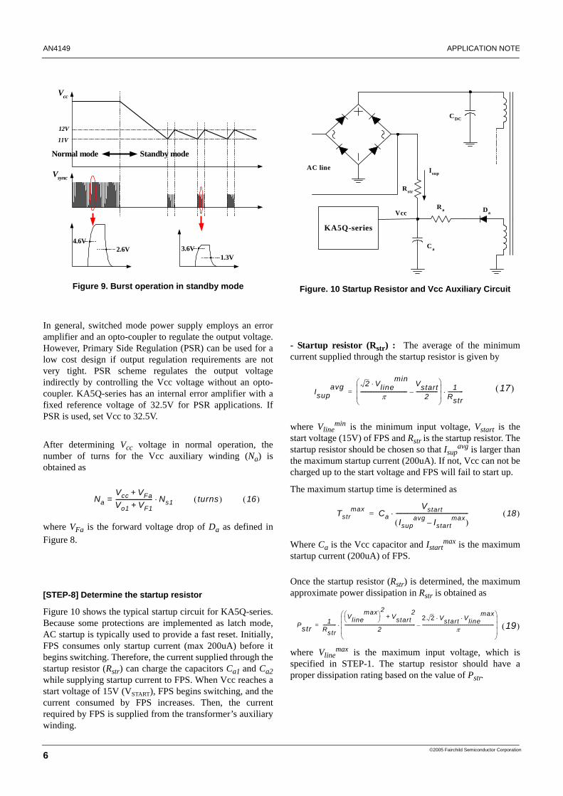
[STEP-8] Determine the startup resistor
Figure 10 shows the typical startup circuit for KA5Q-series.Because some protections are implemented as latch mode,AC startup is typically used to provide a fast reset. Initially,FPS consumes only startup current (max 200uA) before itbegins switching. Therefore, the current supplied through thestartup resistor (Rstr) can charge the capacitors Ca1 and Ca2while supplying startup current to FPS. When Vcc reaches astart voltage of 15V (VSTART), FPS begins switching, and thecurrent consumed by FPS increases. Then, the currentrequired by FPS is supplied from the transformer’s auxiliarywinding.
Figure. 10 Startup Resistor and Vcc Auxiliary Circuit
- Startup resistor (Rstr) : The average of the minimumcurrent supplied through the startup resistor is given by
where Vline
min is the minimum input voltage, Vstart is thestart voltage (15V) of FPS and Rstr is the startup resistor. Thestartup resistor should be chosen so that Isup
avg is larger thanthe maximum startup current (200uA). If not, Vcc can not becharged up to the start voltage and FPS will fail to start up.
The maximum startup time is determined as
Where Ca is the Vcc capacitor and Istartmax is the maximum
startup current (200uA) of FPS.
Once the startup resistor (Rstr) is determined, the maximumapproximate power dissipation in Rstr is obtained as
where Vlinemax is the maximum input voltage, which is
specified in STEP-1. The startup resistor should have aproper dissipation rating based on the value of Pstr.
11V
Standby modeNormal mode
12V
Vcc
Vsync
4.6V2.6V 3.6V
1.3V
NaVcc VFa+Vo1 VF1+--------------------------= Ns1⋅ turns( ) 16( )
KA5Q-series
Rstr
Vcc
Ca
Da
IsupAC line
CDC
Ra
Isupavg 2 Vline
min⋅
π-------------------------------------
Vstart2
-----------------–⎝ ⎠⎜ ⎟⎜ ⎟⎛ ⎞ 1
Rstr------------⋅= 17( )
Tstrmax Ca
Vstart
Isupavg Istart
max–( )---------------------------------------------------⋅= 18( )
Pstr1
Rstr------------
Vlinemax
⎝ ⎠⎛ ⎞
2Vstart
2+
2----------------------------------------------------------------
2 2 Vstart Vlinemax
⋅ ⋅
π-----------------------------------------------------------------–
⎝ ⎠⎜ ⎟⎜ ⎟⎜ ⎟⎛ ⎞
⋅= 19( )
APPLICATION NOTE AN4149
7
©2005 Fairchild Semiconductor Corporation
[STEP-9] Determine the wire diameter for each winding based on the RMS current of each output.
The RMS current of the n-th secondary winding is obtainedas
where Dmax and Idsrms are specified in equations (6) and (9),
Vo(n) is the output voltage of the n-th output, VF(n) is thediode (DR(n)) forward voltage drop, VRO is specified inSTEP-3 and KL(n) is the load occupying factor for n-thoutput defined in equation (2). The current density is typically 5A/mm2 when the wire islong (>1m). When the wire is short with a small number ofturns, a current density of 6-10 A/mm2 is also acceptable. Donot use wire with a diameter larger than 1 mm to avoidsevere eddy current losses as well as to make winding easier. For high current output, it is recommended using parallelwindings with multiple strands of thinner wire to minimizeskin effect.
Check if the winding window area of the core, Aw (refer toFigure 6) is enough to accommodate the wires. The requiredwinding window area (Awr) is given by
where Ac is the actual conductor area and KF is the fill factor.Typically the fill factor is 0.2~0.25 for single outputapplications and 0.15~0.2 for multiple output applications. If the required window (Awr) is larger than the actual windowarea (Aw), go back to the STEP-6 and change the core to abigger one. Sometimes it is impossible to change the coredue to cost or size constraints. In that case, reduce VRO inSTEP-3 or increase fsmin, which reduces the primary sideinductance (Lm) and the minimum number of turns for theprimary (Np
min) as can be seen in equation (7) and (10).
[STEP-10] Choose the proper rectifier diodes in the secondary side based on the voltage and current ratings.The maximum reverse voltage and the rms current of therectifier diode (DR(n)) of the n-th output are obtained as
where KL(n), VDCmax, Dmax and Ids
rms are specified inequations (2), (4), (6) and (9), respectively, VRO is specifiedin STEP-3, Vo(n) is the output voltage of the n-th output andVF(n) is the diode (DR(n)) forward voltage drop. The typical
voltage and current margins for the rectifier diode are asfollows
where VRRM is the maximum reverse voltage and IF is theaverage forward current of the diode.
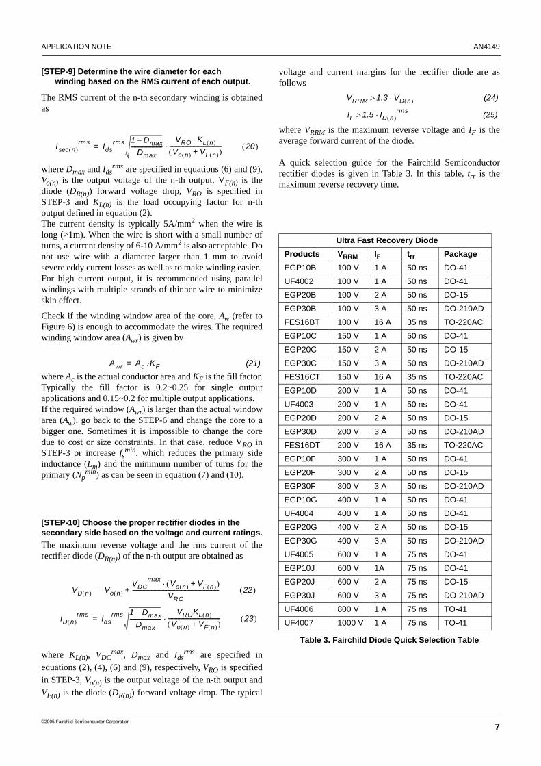
A quick selection guide for the Fairchild Semiconductorrectifier diodes is given in Table 3. In this table, trr is themaximum reverse recovery time.
Table 3. Fairchild Diode Quick Selection Table
I n( )secrms Ids
rms 1 Dmax–Dmax
-----------------------VRO KL n( )⋅
Vo n( ) VF n( )+( )--------------------------------------⋅= 20( )
Awr Ac KF⁄= (21)
VD n( ) Vo n( )VDC
max Vo n( ) VF n( )+( )⋅VRO
----------------------------------------------------------------+= 22( )
ID n( )rms Ids
rms 1 Dmax–Dmax
-----------------------VROKL n( )
Vo n( ) VF n( )+( )--------------------------------------⋅= 23( )
Ultra Fast Recovery DiodeProducts VRRM IF trr PackageEGP10B 100 V 1 A 50 ns DO-41
UF4002 100 V 1 A 50 ns DO-41
EGP20B 100 V 2 A 50 ns DO-15
EGP30B 100 V 3 A 50 ns DO-210AD
FES16BT 100 V 16 A 35 ns TO-220AC
EGP10C 150 V 1 A 50 ns DO-41
EGP20C 150 V 2 A 50 ns DO-15
EGP30C 150 V 3 A 50 ns DO-210AD
FES16CT 150 V 16 A 35 ns TO-220AC
EGP10D 200 V 1 A 50 ns DO-41
UF4003 200 V 1 A 50 ns DO-41
EGP20D 200 V 2 A 50 ns DO-15
EGP30D 200 V 3 A 50 ns DO-210AD
FES16DT 200 V 16 A 35 ns TO-220AC
EGP10F 300 V 1 A 50 ns DO-41
EGP20F 300 V 2 A 50 ns DO-15
EGP30F 300 V 3 A 50 ns DO-210AD
EGP10G 400 V 1 A 50 ns DO-41
UF4004 400 V 1 A 50 ns DO-41
EGP20G 400 V 2 A 50 ns DO-15
EGP30G 400 V 3 A 50 ns DO-210AD
UF4005 600 V 1 A 75 ns DO-41
EGP10J 600 V 1A 75 ns DO-41
EGP20J 600 V 2 A 75 ns DO-15
EGP30J 600 V 3 A 75 ns DO-210AD
UF4006 800 V 1 A 75 ns TO-41
UF4007 1000 V 1 A 75 ns TO-41
VRRM 1.3 VD n( )⋅> (24)
IF 1.5 ID n( )rms⋅> (25)

AN4149 APPLICATION NOTE
8
©2003 Fairchild Semiconductor Corporation
[STEP-11] Determine the output capacitors considering the voltage and current ripple.
The ripple current of the n-th output capacitor (Co(n)) isobtained as
where Io(n) is the load current of the n-th output and ID(n)rms
is specified in equation (23). The ripple current should besmaller than the maximum ripple current specification of thecapacitor. The voltage ripple on the n-th output is given by
where Co(n) is the capacitance, Rc(n) is the effective seriesresistance (ESR) of the n-th output capacitor, KL(n), Dmax andIds
peak are specified in equations (2), (6) and (8) respectively,VRO is specified in STEP-3, Io(n) and Vo(n) are the loadcurrent and output voltage of the n-th output, respectivelyand VF(n) is the diode (DR(n)) forward voltage drop.
Sometimes it is impossible to meet the ripple specificationwith a single output capacitor due to the high ESR of theelectrolytic capacitor. In those cases, additional L-C filterstages (post filter) can be used to reduce the ripple on theoutput.
[STEP-12] Design the synchronization network.
KA5Q-series employs a quasi resonant switching techniqueto minimize the switching noise as well as switching loss. Inthis technique, a capacitor (Cr) is added between theMOSFET drain and source as shown in Figure 11. The basicwaveforms of a quasi-resonant converter are shown in Figure12. The external capacitor lowers the rising slope of drainvoltage, which reduces the EMI caused by the MOSFETturn-off. To minimize the MOSFET switching loss, theMOSFET should be turned on when the drain voltagereaches its minimum value as shown in Figure 12.
The optimum MOSFET turn-on time is indirectly detectedby monitoring the Vcc winding voltage as shown in Figure11 and 12. The output of the sync detect comparator (CO)becomes high when the sync voltage (Vsync) exceeds 4.6Vand low when the Vsync reduces below 2.6V. The MOSFET isturned on at the falling edge of the sync detect comparatoroutput (CO).
Figure. 11 Synchronization Circuit
The peak value of the sync signal is determined by thevoltage divider network RSY1 and RSY2 as
Choose the voltage divider RSY1 and RSY2 so that the peakvalue of sync voltage (Vsync
pk) is lower than the OVPthreshold voltage (12V) in order to avoid triggering OVP innormal operation. Typically, Vsync
pk is set to 8~10V. To synchronize the Vsync with the MOSFET drain voltage,choose the sync capacitor (CSY) so that TF is same as TQ asshown in Figure 12. TF and TQ are given, respectively, as
where Lm is the primary side inductance of the transformer,Ns and Na are the number of turns for the output winding andVcc winding, respectively and Ceo is the effective MOSFEToutput capacitance (Coss+Cr).
Icap n( )rms ID n( )
rms( )2
Io n( )2–= (26)
∆Vo n( )Io n( )Dmax
Co n( )fsmin
--------------------------Ids
peakVRORC n( )KL n( )Vo n( ) VF n( )+( )
----------------------------------------------------------- (27)+=
Vcc
Ca
Da
GND
Cr
Drain
Ids
Rcc
RSY1
RSY2
Sync
Vo1
CSY
+Vds
-
Ns1Np
Lm+
-CO
4.6/2.6V
DSY
Na
KA5Q-series
Vsync
Sync comparator
Vsyncpk RSY2
RSY1 RSY2+---------------------------------- Vcc⋅= 28( )
TF π Lm Ceo⋅⋅= (29)
TQ RSY2 CSYVcc2.6---------
RSY2RSY1 RSY2+----------------------------------⋅⎝ ⎠
⎛ ⎞ln⋅ ⋅= (30)

APPLICATION NOTE AN4149
9
©2005 Fairchild Semiconductor Corporation
Figure. 12 Synchronization Waveforms
[STEP-13] Design voltage drop circuit for the burst operation.
To minimize the power consumption in the standby mode,KA5Q-series employs burst operation. Once FPS enters intoburst mode, all the output voltages as well as effectiveswitching frequencies are reduced as shown in Figure 13.Figure 14 shows the typical output voltage drop circuit forC-TV applications. Under normal operation, the picture onsignal is applied and the transistor Q1 is turned on, which de-couples R3 and D1 from the feedback network. Therefore,only Vo1 is regulated by the feedback circuit in normaloperation and is determined as
In standby mode, the picture on signal is disabled and thetransistor Q1 is turned off, which couples R3 and D1 to thereference pin of KA431. If R3 is small enough to make thereference pin voltage of KA431 higher than 2.5V, the currentthrough the opto LED pulls down the feedback voltage (VFB)of FPS and forces FPS to stop switching. Once FPS stopsswitching, Vcc decreases, and when Vcc reaches 11V, itresumes switching with a predetermined peak drain currentuntil Vcc reaches 12V. When Vcc reaches 12V, the switchingoperation is terminated again until Vcc reduces to 11V. Inthis way, Vcc is hysteresis controlled between 11V and 12Vin the burst mode operation.
Assuming that both Vo1 and Vo2 drop to half of their normalvalues, the maximum value of R3 for proper burst operationis given by
Figure 13. Burst Operation Waveforms
Figure 14. Typical Feedback Circuit to Drop Output Voltage in Standby Mode
[STEP-14] Design the feedback control circuit.Since the KA5Q-series employs current mode control asshown in Figure 15, the feedback loop can be easilyimplemented with a one-pole and one-zero compensationcircuit. The current control factor of FPS, K is defined as
VDC
VRO
VRO
Vds
TF
4.6V
Vsync
TQ
2.6V
Vsyncpk
CO
MOSFET Gate
ONON
Vovp (12V)
Vo1 2.5R1 R2+
R2--------------------⎝ ⎠
⎛ ⎞⋅= (31)
R3V02 2⁄ 0.7– 2.5–( ) R1 R2⋅ ⋅
2.5 R1 R2+( )⋅ R2 V01 2⁄⋅( )–------------------------------------------------------------------------------= (32)
VFB
11V
Standby ModeNormal Mode
12V
Vcc
Ids
Ibpk
1V
Picture ON
MicomLinearRegulator
VO2
VO1 (B+)
KA431R2
R1R3
Rbias
RD
RFCF D1Q1
A
CR

AN4149 APPLICATION NOTE
10
©2005 Fairchild Semiconductor Corporation
where Ipk is the peak drain current and VFB is the feedbackvoltage for a given operating condition, ILIM is the currentlimit of the FPS and VFBsat is the internal feedback saturationvoltage, which is typically 2.5V.
Figure 15. Control Block Diagram
For quasi-resonant flyback converters, the control-to-outputtransfer function using current mode control is given by
where VDC is the DC input voltage, RL is the effective totalload resistance of the controlled output, which is defined asVo1
2/Po. Additionally, Np and Ns1 are specified in STEP-7,VRO is specified in STEP-3, Vo1 is the reference outputvoltage, Po is specified in STEP-1 and K is specified inequation (33). The pole and zeros of equation (34) aredefined as
where Lm is specified in equation (7), D is the duty cycle ofthe FPS, Co1 is the output capacitor of Vo1 and RC1 is theESR of Co1.
When the converter has more than one output, the lowfrequency control-to-output transfer function is proportionalto the parallel combination of all load resistance, adjusted bythe square of the turns ratio. Therefore, the effective loadresistance is used in equation (34) instead of the actual loadresistance of Vo1. Notice that there is a right half plane(RHP) zero (wrz) in the control-to-output transfer function ofequation (34). Because the RHP zero reduces the phase by90 degrees, the crossover frequency should be placed belowthe RHP zero. The Figure 16 shows the variation of a quasi-resonantflyback converter’s control-to-output transfer function fordifferent input voltages. This figure shows the system polesand zeros together with the DC gain change for differentinput voltages. The gain is highest at the high input voltagecondition and the RHP zero is lowest at the low input voltagecondition.
Figure 17 shows the variation of a quasi-resonant flybackconverter’s control-to-output transfer function for differentloads. This figure shows that the gain between fp and fz doesnot change for different loads and the RHP zero is lowest atthe full load condition. The feedback compensation network transfer function ofFigure 15 is obtained as
and RB is the internal feedback bias resistor of FPS, which istypically 2.8kΩ, CTR is the current transfer ratio of optocoupler and R1, RD, RF, CF and CB are shown in Figure 15.
Figure 16. QR Flyback Converter Control-to Output Transfer Function Variation for Different Input Voltages
KIpk
VFB----------
ILIMVFBsat-----------------= = (33)
.ˆˆ 1oFB vandv
In order to express the small signal AC transfer functions,the small signal variations of feedback voltage (vFB) andcontrolled output voltage (vo1) are introduced as
vo1
RD
iDRbias
R1
R2
ibias
CB
vFB
CTR :1
FPSvbias
CFRF
KA431
Ipk
MOSFETcurrent
RB
Gvcvo1vFB---------=
K RLVDC Np Ns1⁄( )⋅2 2VRO vDC+( )
-----------------------------------------------------1 s+ wz⁄( ) 1 s– wrz⁄( )
1 s+ wp⁄----------------------------------------------------------⋅= 34( )
wz1
Rc1Co1--------------------, wrz
RL 1 D–( )2
DLm Ns1 Np⁄( )2----------------------------------------- and wp
1 D+( )RLCo1-------------------= ==
vFBˆ
vo1ˆ--------- -
wis-----
1 s wzc⁄+1 s wpc⁄+--------------------------⋅= 35( )
where wiRB CTR⋅R1RDCF------------------------- , wzc
1RFCF--------------- , wpc
1RBCB---------------===
0 dB
20 dB
-20 dB
-40 dB
40 dB
10Hz 100Hz 10kHz1kHz1Hz 100kHz
Low input voltage
High input voltage
fp
fp
fz
fz frzfrz

APPLICATION NOTE AN4149
11
©2005 Fairchild Semiconductor Corporation
Figure 17. QR Flyback Converter Control-to Output Transfer Function Variation for Different Loads
When the input voltage and the load current vary over a widerange, determining the worst case for the feedback loopdesign is difficult. The gain together with zeros and polesvaries according to the operating conditions.One simple and practical solution to this problem isdesigning the feedback loop for low input voltage and fullload condition with enough phase and gain margin. The RHPzero is lowest at low input voltage and full load condition.The gain increases only about 6dB as the operating conditionis changed from the lowest input voltage to the highest inputvoltage condition under universal input condition.
The procedure to design the feedback loop is as follows
(a) Set the crossover frequency (fc) below 1/3 of RHP zero tominimize the effect of the RHP zero. Set the crossoverfrequency below half of the minimum switching frequency(fsmin).
(b) Determine the DC gain of the compensator (wi/wzc) tocancel the control-to-output gain at fc.
(c) Place a compensator zero (fzc) around fc/3.
(d) Place a compensator pole (fpc) around 3fc.
Figure 18. Compensator Design
When determining the feedback circuit component, there are some restrictions as described below:
(a) Design the voltage divider network of R1 and R2 toprovide 2.5V to the reference pin of the KA431. Therelationship between R1 and R2 is given as
where Vo1 is the reference output voltage.
(b) The capacitor connected to feedback pin (CB) is related to the shutdown delay time in an overload condition by
where VSD is the shutdown feedback voltage and Idelay is theshutdown delay current. Typical values for VSD and Idelayare 7.5V and 5uA, respectively. In general, a delay of 20 ~50 ms is typical for most applications. Because CB alsodetermines the high frequency pole (wpc) of the compensatortransfer function as shown in equation (35), too large a CBcan limit the control bandwidth by placing wpc at too low afrequency. Typical value for CB is 10-50nF. Applicationcircuit to extend the shutdown time without limiting thecontrol bandwidth is shown in Figure 19. By setting thezener breakdown voltage (Vz) slightly higher than 2.7V, theadditional delay capacitor (Cz) is de-coupled from thefeedback circuit in normal operation. When the feedbackvoltage exceeds the zener breakdown voltage (Vz), Cz andCB determine the shutdown time.
Figure 19. Delayed Shutdown
0 dB
20 dB
-20 dB
-40 dB
40 dB
10Hz 100Hz 10kHz1kHz1Hz 100kHz
Heavy load
Light loadfp
fp
fz frzfrz
0 dB
20 dB
-20 dB
-40 dB
40 dB
10Hz 100Hz 10kHz1kHz1Hz 100kHz
Control to output
fp
fz
frz
Compensator
Loop gain T
fzc
fpc
fc
R22.5 R1⋅
Vo1 2.5–------------------------= (36)
Tdelay VSD 2.5–( )= CB⋅ Idelay⁄ (37)
CB
vFB
FPS
IFBIdelay
Cz
Vz
VSD
VZ
2.7V
Tdelay
AN4149 APPLICATION NOTE
12
©2005 Fairchild Semiconductor Corporation
(c) The resistors Rbias and RD used together with the opto-coupler H11A817A and the shunt regulator KA431 shouldbe designed to provide proper operating current for theKA431 and to guarantee the full swing of the feedbackvoltage for the FPS device chosen. In general, the minimumvalues of cathode voltage and current for the KA431 are2.5V and 1mA, respectively. Therefore, Rbias and RD shouldbe designed to satisfy the following conditions:
where Vbias is the KA431 bias voltage as shown in Figure 16and VOP is opto-diode forward voltage drop, which istypically 1V. IFB is the feedback current of FPS, which istypically 1mA.
Vbias VOP– 2.5–RD
--------------------------------------------- IFB> 38( )
VOPRbias-------------- 1mA> (39)
APPLICATION NOTE AN4149
13
©2005 Fairchild Semiconductor Corporation
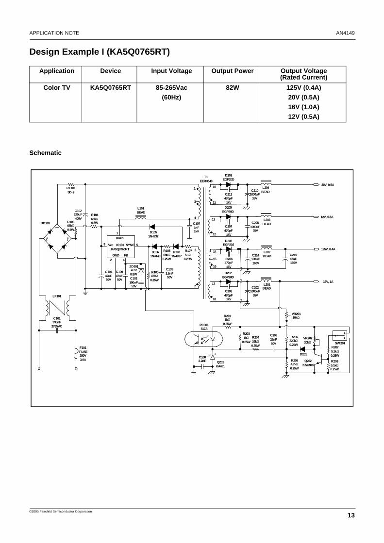
Design Example I (KA5Q0765RT)
Schematic
Application Device Input Voltage Output Power Output Voltage (Rated Current)
Color TV KA5Q0765RT 85-265Vac(60Hz)
82W 125V (0.4A)20V (0.5A)16V (1.0A)12V (0.5A)
C10447uF50V
1
3
4
10
T1EER3540
20V, 0.5A
C2101000uF
35V
D201EGP20D
11
LF101
C101330nF
275VAC
F101 FUSE250V3.0A
C102220uF400V
RT1015D-9
BD101
D1031N4937
R1075.1Ω
0.25W
6
7
R106680Ω0.25W2 4
5
1
3
GND
Drain
SYNC
FB
Vcc
D1061N4148
IC101KA5Q0765RT
C10947nF50V
R105470Ω0.25W
C1053.9nF50V
ZD1014.7V0.5WC103100nF
50V
C1071nF1kV
L101BEAD
D1051N4937
C212470pF
1kV
L204BEAD
12V, 0.5A
D205EGP20D
C2081000uF
35V
13
C207470pF
1kV
L203BEAD
12
125V, 0.4A
D203EGP20J
C214100uF160V
14
C206470pF1kV
L202BEAD
16
C21547uF160V
16V, 1A
D202EGP20D
C2021000uF
35V
17
C205470pF
1kV
L201BEAD
18
PC301817A
R2011kΩ
0.25W
C20322nF50V
C1082.2nF Q201
KA431
R20439kΩ0.25W
R2031kΩ
0.25WR206
220kΩ0.25W
R2054.7kΩ0.25W
VR20130kΩ
D201
VR20230kΩ
Q202KSC945
R2085.1kΩ0.25W
R2075.1kΩ0.25W
SW201
15
R10468kΩ0.5WR103
68kΩ0.5W

AN4149 APPLICATION NOTE
14
©2005 Fairchild Semiconductor Corporation
Transformer Specifications
Transformer Schematic Diagram
Winding Specifications
Electrical Characteristics
Core & BobbinCore : EER 3540Bobbin : EER3540Ae : 109 mm2
No Pin (s→f) Wire Turns Winding MethodNp1 1 - 3 0.6φ × 1 35 Center Winding
N125V/2 16 - 15 0.6φ × 1 28 Center WindingN16V 18 - 17 0.4φ × 2 8 Center WindingN12V 12 - 13 0.5φ × 1 6 Center WindingNp2 3 - 4 0.6φ × 1 35 Center Winding
N125V/2 15 - 14 0.5φ × 1 28 Center WindingN20V 11 - 10 0.5φ × 1 10 Center WindingNa 7 - 6 0.3φ × 1 11 Center Winding
Pin Specification RemarksInductance 1 - 4 565uH ± 5% 1kHz, 1VLeakage Inductance 1 - 4 10uH Max 2nd all short
EER3540
N16V
Na7
13
14
15
16
17
18
N125V/2
N12 V
N20 V
Np1
N p2
1
2
3
4
5
6
8
9 10
11
12
N125V /2
N125V/2
Np2
N12V
N125V/2
N16V
Np1
N20V
Na
APPLICATION NOTE AN4149
15
©2005 Fairchild Semiconductor Corporation
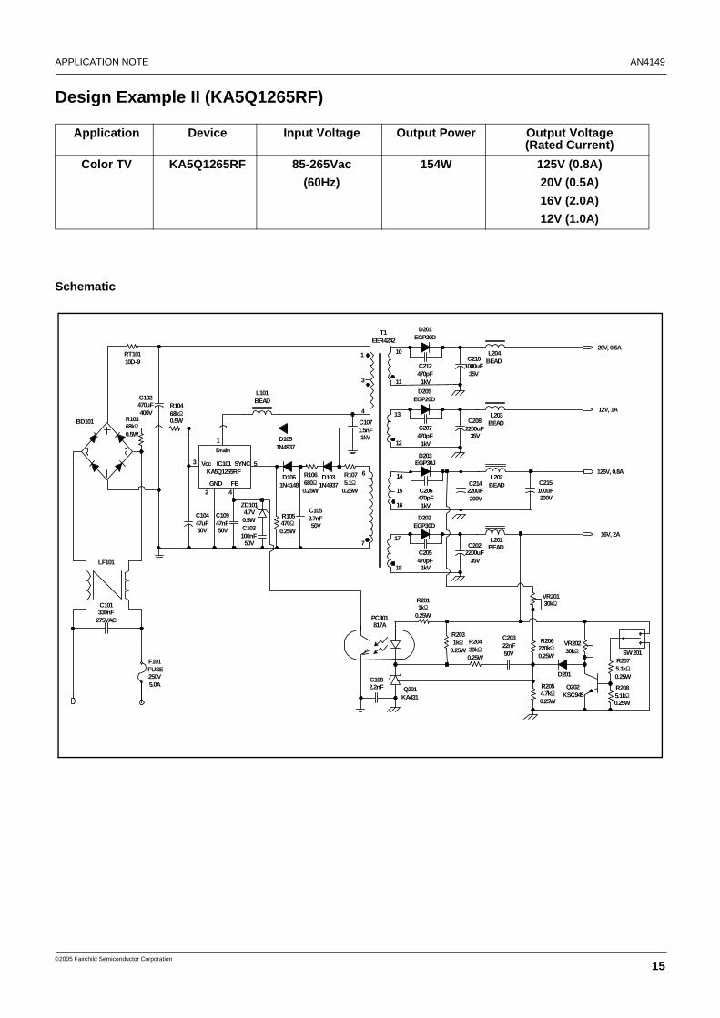
Design Example II (KA5Q1265RF)
Schematic
Application Device Input Voltage Output Power Output Voltage (Rated Current)
Color TV KA5Q1265RF 85-265Vac(60Hz)
154W 125V (0.8A)20V (0.5A)16V (2.0A)12V (1.0A)
C10447uF50V
1
3
4
10
T1EER4242
20V, 0.5A
C2101000uF
35V
D201EGP20D
11
LF101
C101330nF
275VAC
F101 FUSE250V5.0A
C102470uF400V
RT10110D-9
BD101
D1031N4937
R1075.1Ω
0.25W
6
7
R106680Ω0.25W2 4
5
1
3
GND
Drain
SYNC
FB
Vcc
D1061N4148
IC101KA5Q1265RF
C10947nF50V
R105470Ω0.25W
C1052.7nF50V
ZD1014.7V0.5WC103100nF
50V
C1071.5nF1kV
L101BEAD
D1051N4937
C212470pF
1kV
L204BEAD
12V, 1A
D205EGP20D
C2082200uF
35V
13
C207470pF
1kV
L203BEAD
12
125V, 0.8A
D203EGP30J
C214220uF200V
14
C206470pF1kV
L202BEAD
16
C215100uF200V
16V, 2A
D202EGP30D
C2022200uF
35V
17
C205470pF
1kV
L201BEAD
18
PC301817A
R2011kΩ
0.25W
C20322nF50V
C1082.2nF Q201
KA431
R20439kΩ0.25W
R2031kΩ
0.25WR206
220kΩ0.25W
R2054.7kΩ0.25W
VR20130kΩ
D201
VR20230kΩ
Q202KSC945
R2085.1kΩ0.25W
R2075.1kΩ0.25W
SW201
15
R10468kΩ0.5WR103
68kΩ0.5W
AN4149 APPLICATION NOTE
16
©2005 Fairchild Semiconductor Corporation
Transformer Specifications
Transformer Schematic Diagram
Winding Specifications
Electrical Characteristics
Core & BobbinCore : EER 4242Bobbin : EER4242Ae : 234 mm2
No Pin (s→f) Wire Turns Winding MethodNp1 1 - 3 0.5φ × 2 22 Center Winding
N125V/2 16 - 15 0.5φ × 2 18 Center WindingN16V 18 - 17 0.5φ × 2 5 Center WindingN12V 12 - 13 0.4φ × 2 4 Center WindingNp2 3 - 4 0.5φ × 2 22 Center Winding
N125V/2 15 - 14 0.5φ × 2 18 Center WindingN20V 11 - 10 0.5φ × 1 6 Center WindingNa 7 - 6 0.3φ × 1 7 Center Winding
Pin Specification RemarksInductance 1 - 4 385uH ± 5% 1kHz, 1VLeakage Inductance 1 - 4 10uH Max 2nd all short
N125V/2
Np2
N12V
N125V/2
N16V
Np1
N20V
Na
EER4242
N16V
Na7
13
14
15
16
17
18
N125V/2
N12 V
N20 V
Np1
N p2
1
2
3
4
5
6
8
9 10
11
12
N125V /2

APPLICATION NOTE AN4149
17
©2005 Fairchild Semiconductor Corporation
Design Example III (KA5Q1565RF)
Schematic
Application Device Input Voltage Output Power Output Voltage (Rated Current)
Color TV KA5Q1565RF 85-265Vac(60Hz)
217W 125V (1.0A)20V (1.0A)16V (3.0A)12V (2.0A)
C10447uF50V
1
3
4
10
T1EER5345
20V, 1A
C2101000uF
35V
D201EGP20D
11
LF101
C101330nF
275VAC
F101 FUSE250V5.0A
C102470uF400V
RT10110D-9
BD101
D1031N4937
R1075.1Ω
0.25W
6
7
R106680Ω0.25W2 4
5
1
3
GND
Drain
SYNC
FB
Vcc
D1061N4148
IC101KA5Q1565RF
C10947nF50V
R105470Ω0.25W
C1052.7nF50V
ZD1014.7V0.5WC103100nF
50V
C1072nF1kV
L101BEAD
D1051N4937
C212470pF
1kV
L204BEAD
12V, 2A
D205EGP30D
C2082200uF
35V
13
C207470pF
1kV
L203BEAD
12
125V, 1A
D203FFPF05U60S
C214330uF200V
14
C206470pF1kV
L202BEAD
16
C215220uF200V
16V, 3A
D202FFPF05U20S
C2022200uF
35V
17
C205470pF
1kV
L201BEAD
18
PC301817A
R2011kΩ
0.25W
C20322nF50V
C1082.2nF Q201
KA431
R20439kΩ0.25W
R2031kΩ
0.25WR206
220kΩ0.25W
R2054.7kΩ0.25W
VR20130kΩ
D201
VR20230kΩ
Q202KSC945
R2085.1kΩ0.25W
R2075.1kΩ0.25W
SW201
15
R10468kΩ0.5WR103
68kΩ0.5W
AN4149 APPLICATION NOTE
18
©2005 Fairchild Semiconductor Corporation
Transformer Specifications
Transformer Schematic Diagram
Winding Specifications
Electrical Characteristics
Core & BobbinCore : EER 5345Bobbin : EER5345Ae : 318 mm2
No Pin (s→f) Wire Turns Winding MethodNp1 1 - 3 0.6φ × 2 21 Center Winding
N125V/2 16 - 15 0.6φ × 2 17 Center WindingN16V 18 - 17 0.6φ × 3 5 Center WindingN12V 12 - 13 0.6φ × 2 4 Center WindingNp2 3 - 4 0.6φ × 2 21 Center Winding
N125V/2 15 - 14 0.6φ × 2 17 Center WindingN20V 11 - 10 0.5φ × 1 6 Center WindingNa 7 - 6 0.3φ × 1 7 Center Winding
Pin Specification RemarksInductance 1 - 4 325uH ± 5% 1kHz, 1VLeakage Inductance 1 - 4 10uH Max 2nd all short
EER5345
N16V
Na7
13
14
15
16
17
18
N125V/2
N12 V
N20 V
Np1
N p2
1
2
3
4
5
6
8
9 10
11
12
N125V/2
N125V/2
Np2
N12V
N125V/2
N16V
Np1
N20V
Na
AN4149 APPLICATION NOTE
9/20/05 0.0m 002© 2005 Fairchild Semiconductor Corporation
DISCLAIMER FAIRCHILD SEMICONDUCTOR RESERVES THE RIGHT TO MAKE CHANGES WITHOUT FURTHER NOTICE TO ANY PRODUCTS HEREIN TO IMPROVE RELIABILITY, FUNCTION OR DESIGN. FAIRCHILD DOES NOT ASSUME ANY LIABILITY ARISING OUT OF THE APPLICATION OR USE OF ANY PRODUCT OR CIRCUIT DESCRIBED HEREIN; NEITHER DOES IT CONVEY ANY LICENSE UNDER ITS PATENT RIGHTS, NOR THE RIGHTS OF OTHERS.
LIFE SUPPORT POLICY FAIRCHILD’S PRODUCTS ARE NOT AUTHORIZED FOR USE AS CRITICAL COMPONENTS IN LIFE SUPPORT DEVICES OR SYSTEMS WITHOUT THE EXPRESS WRITTEN APPROVAL OF THE PRESIDENT OF FAIRCHILD SEMICONDUCTOR CORPROATION. As used herein:
1. Life support devices or systems are devices or systems which, (a) are intended for surgical implant into the body, or (b) support or sustain life, or (c) whose failure to perform when properly used in accordance with instructions for use provided in the labeling, can be reasonably expected to result in significant injury to the user.
2. A critical component is any component of a life support device or system whose failure to perform can be reasonably expected to cause the failure of the life support device or system, or to affect its safety or effectiveness.
www.fairchildsemi.com
Hangseok Choi, Ph.DPower Conversion Team / Fairchild SemiconductorPhone : +82-32-680-1383 Facsimile : +82-32-680-1317E-mail : [email protected]

www.onsemi.com1
ON Semiconductor and are trademarks of Semiconductor Components Industries, LLC dba ON Semiconductor or its subsidiaries in the United States and/or other countries.ON Semiconductor owns the rights to a number of patents, trademarks, copyrights, trade secrets, and other intellectual property. A listing of ON Semiconductor’s product/patentcoverage may be accessed at www.onsemi.com/site/pdf/Patent−Marking.pdf. ON Semiconductor reserves the right to make changes without further notice to any products herein.ON Semiconductor makes no warranty, representation or guarantee regarding the suitability of its products for any particular purpose, nor does ON Semiconductor assume any liabilityarising out of the application or use of any product or circuit, and specifically disclaims any and all liability, including without limitation special, consequential or incidental damages.Buyer is responsible for its products and applications using ON Semiconductor products, including compliance with all laws, regulations and safety requirements or standards,regardless of any support or applications information provided by ON Semiconductor. “Typical” parameters which may be provided in ON Semiconductor data sheets and/orspecifications can and do vary in different applications and actual performance may vary over time. All operating parameters, including “Typicals” must be validated for each customerapplication by customer’s technical experts. ON Semiconductor does not convey any license under its patent rights nor the rights of others. ON Semiconductor products are notdesigned, intended, or authorized for use as a critical component in life support systems or any FDA Class 3 medical devices or medical devices with a same or similar classificationin a foreign jurisdiction or any devices intended for implantation in the human body. Should Buyer purchase or use ON Semiconductor products for any such unintended or unauthorizedapplication, Buyer shall indemnify and hold ON Semiconductor and its officers, employees, subsidiaries, affiliates, and distributors harmless against all claims, costs, damages, andexpenses, and reasonable attorney fees arising out of, directly or indirectly, any claim of personal injury or death associated with such unintended or unauthorized use, even if suchclaim alleges that ON Semiconductor was negligent regarding the design or manufacture of the part. ON Semiconductor is an Equal Opportunity/Affirmative Action Employer. Thisliterature is subject to all applicable copyright laws and is not for resale in any manner.
PUBLICATION ORDERING INFORMATIONN. American Technical Support: 800−282−9855 Toll FreeUSA/Canada
Europe, Middle East and Africa Technical Support:Phone: 421 33 790 2910
Japan Customer Focus CenterPhone: 81−3−5817−1050
www.onsemi.com
LITERATURE FULFILLMENT:Literature Distribution Center for ON Semiconductor19521 E. 32nd Pkwy, Aurora, Colorado 80011 USAPhone: 303−675−2175 or 800−344−3860 Toll Free USA/CanadaFax: 303−675−2176 or 800−344−3867 Toll Free USA/CanadaEmail: [email protected]
ON Semiconductor Website: www.onsemi.com
Order Literature: http://www.onsemi.com/orderlit
For additional information, please contact your localSales Representative
© Semiconductor Components Industries, LLC