THERMOMECHANICAL DATA STORAGE
A SEMINAR REPROT
Submitted by
KANHAIYA KUMAR
in partial fulfillment for the award of the degree
Of
BACHELOR OF TECHNOLOGY
in
COMPUTER SCIENCE & ENGINEERING
SCHOOL OF ENGINEERING
COCHIN UNIVERSITY OF SCIENCE & TECHNOLOGY
KOCHI-682022
SEPTEMBER-2010
ACKNOWLEDGEMENT
We take this occasion to thank God, Almighty for blessing us with his
grace and taking our endeavor to a successful culmination. We extend our
sincere and heartfelt thanks to our esteemed guide, Ms. Anu M. for
providing us with the right guidance and advice at the crucial junctures
and for showing us the right way. We extend our sincere thanks to our
respected head of the division Dr. David Peter , for allowing us to use
the facilities available. We would also like to thank the our class co-
ordinator Mr. Sudheep Elayidom for his kind suggestion towards the
initiative of this seminar.We would like to thank the other faculty
members also,at this occasion. Last but not least we would like to thank
friends for the support and encouragement they have given us during the
course of our work.
KANHAIYA KUMAR
Reg No:-12080036
i
ABSTRACT
In the future, the current method of magnetically storing data may reach its
limit of maximum achievable density. Hence we need a data storage
technology which has high storage capacity and is small in size. The solution is
Thermomechanical data storage. Thermomechanical Data Storage is a data
storage scheme in which nanometer sized pits on a plastic disc represent digital
data. This data storage concept combines ultrahigh density, terabit capacity,
small form factor and high data rates. By using this concept, we will be able to
store the equivalent of 25 DVDs on a surface the size of a postage stamp. IBM
scientists have demonstrated a data storage density of a trillion bits per square
inch - 20 times higher than the densest magnetic storage available today. IBM
achieved this remarkable density -- enough to store 25 million printed textbook
pages on a surface the size of a postage stamp -- in a research project code-
named "Millipede". Millipede uses thousands of nano-sharp tips to punch
indentations representing individual bits into a thin plastic film. The result is
akin to a nanotech version of the venerable data processing 'punch card'
developed more than 110 years ago, but with two crucial differences: the
'Millipede' technology is re-writeable, and may be able to store more than 3
billion bits its of data in the space occupied by just one hole in a standard
punch card
ii
CONTENTS
ACKNOWLEDGEMENT…………………………………………..i
ABSTRACT………………………………………………………..ii
1. INTRODUCTION ………………………………………. 1
2. THERMOMECHANICAL AFM DATA STORAGE….. 4
2. 1 DATA WRITING……………………………………………………… 4
2.2 DATA READING……………………………………………………… 7
3. THE MILLIPEDE CONCEPT …………………………. 9
4. CANTILEVER DESIGN AND FABRICATION………. 13
5. ARRAY DESIGN, TECHNOLOGY, FABRICATION… 17
6. ARRAY CHARECTERIZATION………………………. 19
7. THE POLYMER MEDIUM……………………………… 20
8. DATA ERASING………………………………………….. 27
9. ADVANTAGES……………………………………………. 29
10. CONCLUSION…………………………………………….. 30
11. REFERENCES…………………………………………….. 31
iii
LIST OF SYMBOLS AND ABBREVATIONS
PMMA- POLYMETHYLMETHAACRYLATE
SI- SILICON
AFM- ATOMIC FORCE MICROSCOPY
IBM- INTERNATIONAL BUSINESS MACHINE
SOE- SCHOOL OF ENGINEERING
CUSAT- COCHIN UNIVERSITY OF SCIENCE AND TECHNOLOGY
iv
Thermomechanical data storage
1 .INTRODUCTION
In the 21st century, the nanometer will very likely play a role similar to the
one played by the micrometer in the 20th century The nanometer scale will presumably
pervade the field of data storage. In magnetic storage today, there is no clear-cut way to
achieve the nanometer scale in all three dimensions. The basis for storage in the 21st
century might still be magnetism. Within a few years, however, magnetic storage
technology will arrive at a stage of its exciting and successful evolution at which
fundamental changes are likely to occur when current storage technology hits the well-
known superparamagnetic limit. Several ideas have been proposed on how to overcome
this limit. One such proposal involves the use of patterned magnetic media. Other
proposals call for totally different media and techniques such as local probes or
holographic methods. Similarly, consider Optical lithography. Although still the
predominant technology, it will soon reach its fundamental limits and be replaced by a
technology yet unknown. In general, if an existing technology reaches its limits in the
course of its evolution and new alternatives are emerging in parallel, two things usually
happen: First, the existing and well-established technology will be explored further and
everything possible done to push its limits to take maximum advantage of the
considerable investments made. Then, when the possibilities for improvements have
been exhausted, the technology may still survive for certain niche applications, but the
emerging technology will take over, opening up new perspectives and new directions.
Today we are witnessing in many fields the transition from structures of the
micrometer scale to those of the nanometer scale, a dimension at which nature has long
been building the finest devices with a high degree of local functionality. Many of the
technologies we use today are not suitable for the
Division of Computer engineering, SOE 1
Thermomechanical data storage
coming nanometer age; some will require minor or major modifications, and others will
be partially or entirely replaced. It is certainly difficult to predict which techniques will
fall into which category. For key areas in information-technology hardware it is not yet
obvious which technology and materials will be used for nanoelectronics and data
storage.
In any case, an emerging technology being considered as a serious candidate
to replace an existing but limited technology must offer long-term perspectives. For
instance, the silicon microelectronics and storage industries are huge and require
correspondingly enormous investments, which makes them long-term oriented by
nature, The consequence for storage is that any new technique with better areal storage
density than today’s magnetic recording should have long term potential for further
scaling, desirably down to the nanometer or even atomic scale.
The only available tool known today that is simple and yet provides these
very long term perspectives is a nanometer sharp tip. Such tips are now being used in
every atomic force microscope (AFM) and scanning tunneling microscope (STM) for
imaging and structuring down to the atomic scale. The simple tip is a very reliable tool
that concentrates on one functionality: the ultimate local confinement of interaction.
In the early 90's, Mamin and Rugar at the IBM Almaden Research Center
pioneered the possibility of using an AFM tip for read back and writing of topographic
features for the purposes of data storage. In one scheme developed by them, reading
and writing were demonstrated with a single AFM tip in contact with a rotating
polycarbonate substrate. The writing was done thermomechanically via heating of the
tip. In this way, storage densities of up to 30Gb/in2 were achieved, representing a
significant advance compared to the densities of that day. Later refinements included
increasing readback speeds up to a data rate of 10 Mb/s, and implementation of track
servoing.
Division of Computer engineering, SOE 2
Thermomechanical data storage
In making use of single tips in AFM or STM operation for storage, one has to deal with
their fundamental limits for high data rates. The mechanical resonant frequencies of the
AFM cantilevers limit the data rates of a single cantilever to a few Mb/s for AFM data
storage, and the feedback speed and low tunneling currents limit STM-based storage &
approaches to even lower data rates. Currently a single AFM operates at best on the
microsecond time scale. Conventional magnetic storage, however, operates at best on
the nanosecond time scale, making it clear that AFM data rates have to be improved by
at least three orders of magnitudes to be competitive with current and future magnetic
recording. Later, it was found that by operating the AFM tips in parallel, data storage
with areal storage densities far beyond the expected superparamagnetic limit (~100
Gb/in2) and data rates comparable to those of today's magnetic recording can be
achieved.
The "Millipede” concept which will be discussed here is a new approach for
storing data at high speed and with an ultrahigh density. It is not a modification of an
existing storage technology, although the use of magnetic materials as storage medium
is not excluded. The ultimate locality is given by a tip, and high data rates are a result
of massive parallel operation of such tips. Using this Millipede concept areal densities
up to 0.5-1 Tb/in2 can be achieved by the parallel operation of very large 2D (32 x
32) AFM cantilever arrays with integrated tips and write/read storage functionality.
The fabrication and integration of such a large number of mechanical devices
(cantilever beams) will lead to what we envision as the VLSI age of micro/
nanomechanics. It is our conviction that VLSI micro/nanomechanics will greatly
complement future micro and nanoelectronics (integrated or hybrid) and may generate
applications of VLSI-MEMS (VLSI-MicroElectroMechanical Systems) not conceived
of today.
Division of Computer engineering, SOE 3
Thermomechanical data storage
2 .THERMOMECHANICAL AFM DATA STORAGE
In recent years, AFM thermomechanical recording in polymer storage media
has undergone extensive modifications mainly with respect to the integration of sensors
and heaters designed to enhance simplicity and to increase data rate and storage
density. Using these heater cantilevers, high storage density and data rates have been
achieved. Let us now describe the storage operations in detail.
2. 1. DATA WRITING
Thermomechanical writing is a combination of applying a local force by the
cantilever/tip to the polymer layer, and softening it by local heating. Initially, the heat
transfer from the tip to the polymer through the small contact area is very poor and
improves as the contact area increases. This means the tip must be heated to a relatively
high temperature (about 400oC) to initiate the softening. Once softening has
commenced, the tip is pressed into the polymer, which increases the heat transfer to the
polymer, increases the volume of softened polymer, and hence increases the bit size.
Our rough estimates indicate that at the beginning of the writing process only about
0.2% of the heating power is used in the very small contact zone (10-40 nm2) to soften
the polymer locally, whereas about 80% is lost through the cantilever legs to the chip
body and about 20% is radiated from the heater platform through the air gap to the
medium/substrate. After softening has started and the contact area has increased, the
heating power available for generating the indentations increases by at least ten times
to become 2% or more of the total heating power.
Division of Computer engineering, SOE 4
Thermomechanical data storage
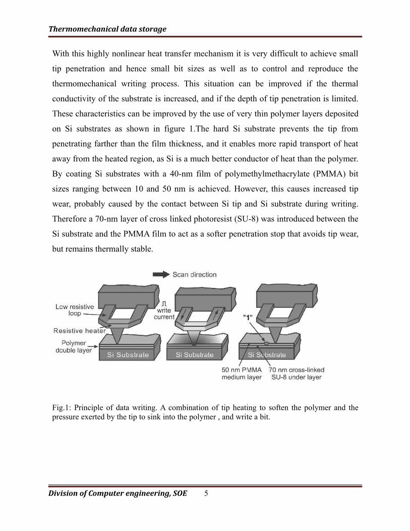
With this highly nonlinear heat transfer mechanism it is very difficult to achieve small
tip penetration and hence small bit sizes as well as to control and reproduce the
thermomechanical writing process. This situation can be improved if the thermal
conductivity of the substrate is increased, and if the depth of tip penetration is limited.
These characteristics can be improved by the use of very thin polymer layers deposited
on Si substrates as shown in figure 1.The hard Si substrate prevents the tip from
penetrating farther than the film thickness, and it enables more rapid transport of heat
away from the heated region, as Si is a much better conductor of heat than the polymer.
By coating Si substrates with a 40-nm film of polymethylmethacrylate (PMMA) bit
sizes ranging between 10 and 50 nm is achieved. However, this causes increased tip
wear, probably caused by the contact between Si tip and Si substrate during writing.
Therefore a 70-nm layer of cross linked photoresist (SU-8) was introduced between the
Si substrate and the PMMA film to act as a softer penetration stop that avoids tip wear,
but remains thermally stable.
Fig.1: Principle of data writing. A combination of tip heating to soften the polymer and the pressure exerted by the tip to sink into the polymer , and write a bit.
Division of Computer engineering, SOE 5
Thermomechanical data storage
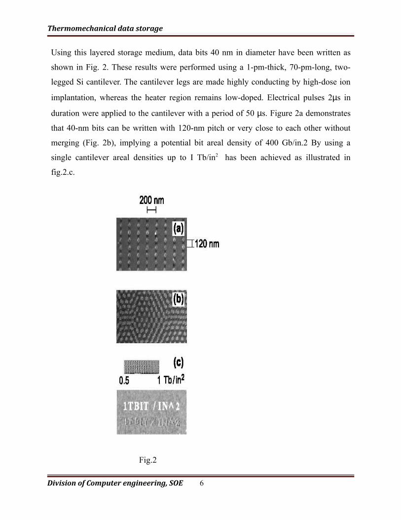
Using this layered storage medium, data bits 40 nm in diameter have been written as
shown in Fig. 2. These results were performed using a 1-pm-thick, 70-pm-long, two-
legged Si cantilever. The cantilever legs are made highly conducting by high-dose ion
implantation, whereas the heater region remains low-doped. Electrical pulses 2µs in
duration were applied to the cantilever with a period of 50 µs. Figure 2a demonstrates
that 40-nm bits can be written with 120-nm pitch or very close to each other without
merging (Fig. 2b), implying a potential bit areal density of 400 Gb/in.2 By using a
single cantilever areal densities up to I Tb/in2 has been achieved as illustrated in
fig.2.c.
Fig.2
Division of Computer engineering, SOE 6
Thermomechanical data storage
2.2 DATA READING
Imaging and reading are done using a new thermomechanical sensing concept. The
heater cantilever originally used only for writing was given the additional function of a
thermal readback sensor by exploiting its temperature-dependent resistance. 'The
resistance (R) increases nonlinearly with heating power/temperature from room
temperature to a peak value of 500-7000oC. The peak temperature is determined by the
doping concentration of the heater platform, which ranges from 1x10¹⁷ to 2x10¹⁸.Above
the peak temperature, the resistance drops as the number of intrinsic carriers increases
because of thermal excitation. For sensing, the resistor is operated at about 350oC, a
temperature that is not high enough to soften the polymer as is the case for writing. The
principle of thermal sensing is based on the fact that the thermal conductance between
the heater platform and the storage substrate changes according to the distance between
them. The medium between a cantilever and the storage substrate -in our case air-
transports heat from one side to the other. When the distance between heater and
sample is reduced as the tip moves into a bit indentation, the heat transport through air
will be more efficient, and the heater's temperature and hence its resistance will
decrease. Thus, changes in temperature of the continuously heated resistor are
monitored while the cantilever is scanned over data bits, providing a means of
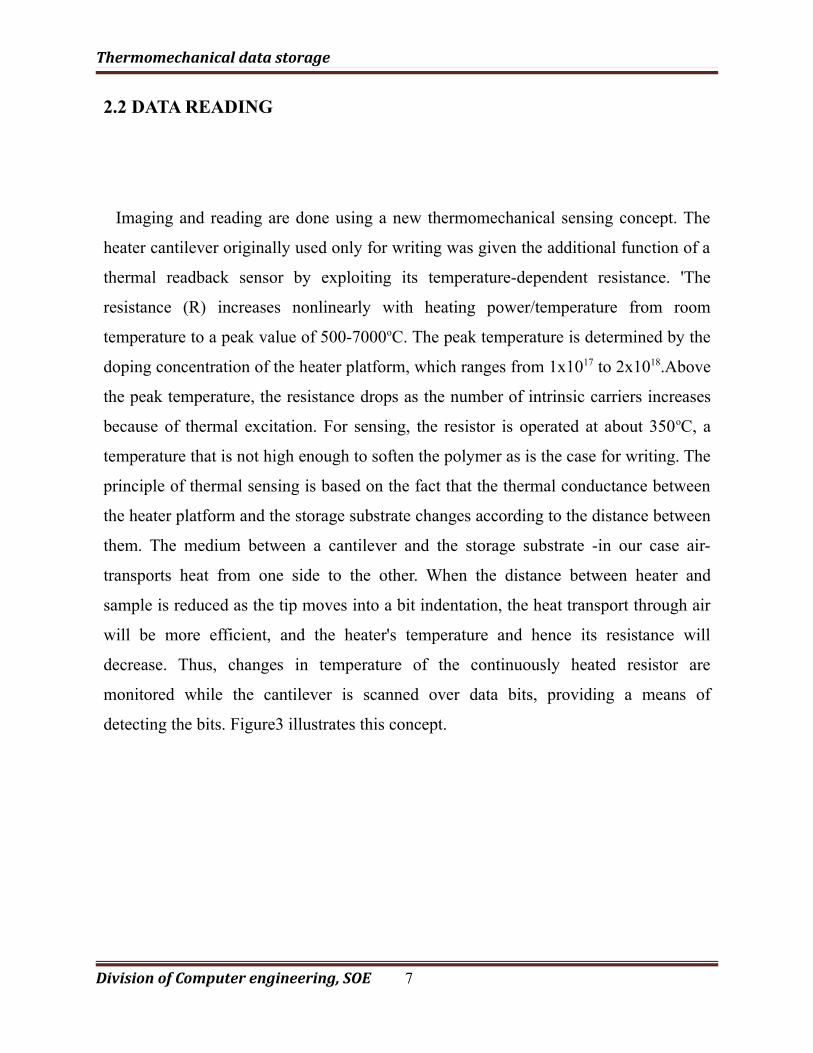
detecting the bits. Figure3 illustrates this concept.
Division of Computer engineering, SOE 7
Thermomechanical data storage
Fig.3: Principle of AFM thermal sensing. The tip of the heater cantilever is continuously heated by a dc power supply while the cantilever is being scanned and the heater resistivity measured.
Under typical operating conditions, the sensitivity of thermomechanical
sensing is even better than that of piezoresistive -strain sensing, which is not surprising
because thermal effects in semiconductors are stronger than strain effects. The good
∆R/R sensitivity of about 10-5/nm is demonstrated by tile images of the 40 nm size bit
indentations in Fig. 2 which have been obtained using the described thermal-sensing
technique.
The data erasing operation will be discussed while explaining the polymer
material used as the storage medium.
Division of Computer engineering, SOE 8
Thermomechanical data storage
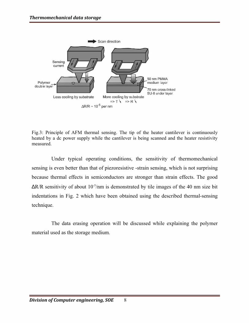
3. THE MILLIPEDE CONCEPT
The 2D AFM cantilever array storage technique called "Millipede" is
illustrated in Fig. 4.
Millipede uses thousands of nano-sharp tips to punch indentations
representing individual bits into a thin plastic film.
Fig.4: The Millipede Concept
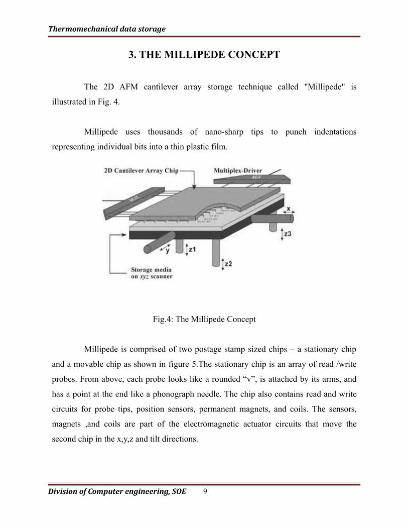
Millipede is comprised of two postage stamp sized chips – a stationary chip
and a movable chip as shown in figure 5.The stationary chip is an array of read /write
probes. From above, each probe looks like a rounded “v”, is attached by its arms, and
has a point at the end like a phonograph needle. The chip also contains read and write
circuits for probe tips, position sensors, permanent magnets, and coils. The sensors,
magnets ,and coils are part of the electromagnetic actuator circuits that move the
second chip in the x,y,z and tilt directions.
Division of Computer engineering, SOE 9
Thermomechanical data storage
Fig.5: A section of IBM Millipede MEMS based storage chips
The movable chip is the storage medium. The electromagnetic actuators move
the storage medium over the stationary medium, which contains the cantilevers for
write/read operations, in x and y directions. The storage area looks like a 32x32
checkerboard where a square in the checkerboard contains a million bits. Each probe
reads and writes only in its square.
Millipede is based on a mechanical parallel x/y scanning of either the entire cantilever
array chip or the storage medium. In addition, a feedback-controlled z-approaching and
Division of Computer engineering, SOE 10
Thermomechanical data storage
leveling scheme brings the entire cantilever array chip into contact with the storage
medium. This tip-medium contact is maintained and controlled while x/y scanning is
performed for write/read. It is important to note that the Millipede approach is not
based on individual z-feedback for each cantilever; rather, it uses a feedback control for
the entire chip, which greatly simplifies the system. However, this requires very good
control and uniformity of tip height and cantilever bending. Chip approach/leveling
makes use of additionally integrated approaching cantilever sensors in the corners of
the array chip to control the approach of the chip to the storage medium. Signals from
these sensors provide feedback signals to adjust the z-actuators until contact with the
medium is established. The system operates similarly to an antivibration table.
Feedback loops maintain the chip leveled and in contact with the surface while x/y
scanning is performed for write/read operations. This basic concept of the entire chip
approach/leveling has been tested and demonstrated for the first time by parallel
imaging with a 5x5 array chip. These parallel imaging results have shown that all 25
cantilever tips have approached the substrate within less than 1 µm of z-activation. This
promising result convinced us that chips tip-apex height control of less than 500 nm is
feasible. This stringent requirement for tip-apex uniformity over the entire chip is
determined by the uniform force required to minimize/eliminate tip and medium wear
due to large force variations resulting from large tip-height nonuniformities.
During the storage operation, the chip is raster-scanned over an area called the
storage field by a magnetic x/y scanner. The scanning distance is equivalent to the
cantilever x/y pitch, which is currently 92 pm. Each cantilever/tip of the array writes and
reads data only in its own storage field. This eliminates the need for lateral positioning
adjustments of the tip to offset lateral position tolerances in tip fabrication. Consequently,
a 32x32 array chip will generate 32x32 (1024) storage fields on an area of less than 3x3
mm2 Assuming an areal density of 500 Gb/in2, one storage field of 92x92 µm2 has a
capacity of 0.875 MB and the entire 32x32 array with 1024 storage fields has a capacity
Division of Computer engineering, SOE 11
Thermomechanical data storage
of 0.9 GB 3 x 3 mm2. The storage capacity of the system scales with the areal density,
the cantilever pitch (storage-field size), and the number of cantilevers in the array.
Although not yet investigated in detail, lateral tracking will also be performed for the
entire chip with integrated tracking
sensors at the chip periphery. This assumes and requires very good temperature1
control of the array chip and the medium substrate between write and read cycles. For
this reason the array chip and medium substrate should be held within about 1oC
operating temperature for bit sizes of 30 to 40 nm and array chip sizes of a few
millimeters. This will be achieved by using the same material (silicon) for both the
array chip and the medium substrate in conjunction with four integrated heat sensors
that control four heaters on the chip to maintain a constant array chip temperature
during operation. True parallel operation of large 2D arrays results in very large chip
sizes because of the space required for the individual write/read wiring to each
cantilever and the many I/O pads. The row/column time-multiplexing addressing
scheme implemented successfully in every DRAM is a very elegant solution to this
issue. In the case of Millipede, the time-multiplexed addressing scheme is used to
address the array row by row with full parallel write/read operation within one row.
The current Millipede storage approach is based on a new thermomechanical
write/read process in nanometer thick polymer films, but thermomechanical writing in
polycarbonate films and optical readback was first investigated and demonstrated by
Mamin and Rugar. Although the storage density of 30 Gb/in.2 obtained originally was not
overwhelming, the results encouraged us to use polymer films as well to achieve density
improvements.
Division of Computer engineering, SOE 12
Thermomechanical data storage
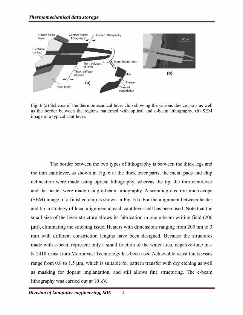
4. CANTILEVER DESIGN AND FABRICATION
The cantilever chip (see Fig. 6) consists of a chip body with large metal pads
for electrical contact, thick and mechanically stiff cantilever legs, and the thin
cantilever itself, which corresponds to a cantilever as found in a Millipede array. The
main part that influences power consumption and data rate of the cantilever is the
heater / tip area. For this study, the heater dimensions as well as those of the two
thermal constrictions on both heater sides will be varied. The thick legs allow some
clearance to the chip body to facilitate the approaching procedure as well as a well-
defined cantilever anchor position. Their stiffness is 30 times that of the cantilever, thus
they are considered a perfect anchor.
The entire cantilever structure consists of monocrystalline silicon, ensuring
thermal and mechanical stability, which is crucial for a cantilever used for
thermomechanical writing / reading.
Division of Computer engineering, SOE 13
Thermomechanical data storage
Fig. 6 (a) Schema of the thermomecanical lever chip showing the various device parts as well as the border between the regions patterned with optical and e-beam lithography. (b) SEM image of a typical cantilever.
The border between the two types of lithography is between the thick legs and
the thin cantilever, as shown in Fig. 6 a: the thick lever parts, the metal pads and chip
delineation were made using optical lithography, whereas the tip, the thin cantilever
and the heater were made using e-beam lithography. A scanning electron microscope
(SEM) image of a finished chip is shown in Fig. 6 b. For the alignment between heater
and tip, a strategy of local alignment at each cantilever cell has been used. Note that the
small size of the lever structure allows its fabrication in one e-beam writing field (200
µm), eliminating the stitching issue. Heaters with dimensions ranging from 200 nm to 3
mm with different constriction lengths have been designed. Because the structures
made with e-beam represent only a small fraction of the wafer area, negative-tone ma-
N 2410 resist from Microresist Technology has been used Achievable resist thicknesses
range from 0.8 to 1.5 µm, which is suitable for pattern transfer with dry etching as well
as masking for dopant implantation, and still allows fine structuring. The e-beam
lithography was carried out at 10 kV.
Division of Computer engineering, SOE 14
Thermomechanical data storage
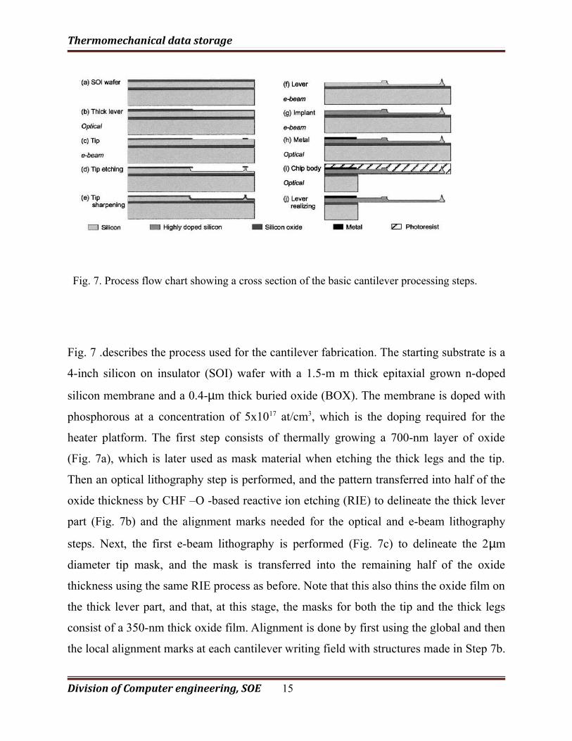
Fig. 7. Process flow chart showing a cross section of the basic cantilever processing steps.
Fig. 7 .describes the process used for the cantilever fabrication. The starting substrate is a
4-inch silicon on insulator (SOI) wafer with a 1.5-m m thick epitaxial grown n-doped
silicon membrane and a 0.4-µm thick buried oxide (BOX). The membrane is doped with
phosphorous at a concentration of 5x10¹⁷ at/cm3, which is the doping required for the
heater platform. The first step consists of thermally growing a 700-nm layer of oxide
(Fig. 7a), which is later used as mask material when etching the thick legs and the tip.
Then an optical lithography step is performed, and the pattern transferred into half of the
oxide thickness by CHF –O -based reactive ion etching (RIE) to delineate the thick lever
part (Fig. 7b) and the alignment marks needed for the optical and e-beam lithography
steps. Next, the first e-beam lithography is performed (Fig. 7c) to delineate the 2µm
diameter tip mask, and the mask is transferred into the remaining half of the oxide
thickness using the same RIE process as before. Note that this also thins the oxide film on
the thick lever part, and that, at this stage, the masks for both the tip and the thick legs
consist of a 350-nm thick oxide film. Alignment is done by first using the global and then
the local alignment marks at each cantilever writing field with structures made in Step 7b.
Division of Computer engineering, SOE 15
Thermomechanical data storage
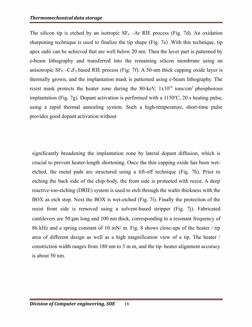
The silicon tip is etched by an isotropic SF6 –Ar RIE process (Fig. 7d). An oxidation
sharpening technique is used to finalize the tip shape (Fig. 7e) .With this technique, tip
apex radii can be achieved that are well below 20 nm. Then the lever part is patterned by
e-beam lithography and transferred into the remaining silicon membrane using an
anisotropic SF6 –C4F8 based RIE process (Fig. 7f). A 50-nm thick capping oxide layer is
thermally grown, and the implantation mask is patterned using e-beam lithography. The
resist mask protects the heater zone during the 80-keV, 1x10¹⁶ ions/cm2 phosphorous
implantation (Fig. 7g). Dopant activation is performed with a 1150oC, 20 s heating pulse,
using a rapid thermal annealing system. Such a high-temperature, short-time pulse
provides good dopant activation without
significantly broadening the implantation zone by lateral dopant diffusion, which is
crucial to prevent heater-length shortening. Once the thin capping oxide has been wet-
etched, the metal pads are structured using a lift-off technique (Fig. 7h). Prior to
etching the back side of the chip body, the front side is protected with resist. A deep
reactive-ion-etching (DRIE) system is used to etch through the wafer thickness with the
BOX as etch stop. Next the BOX is wet-etched (Fig. 7i). Finally the protection of the
resist front side is removed using a solvent-based stripper (Fig. 7j). Fabricated
cantilevers are 50 µm long and 100 nm thick, corresponding to a resonant frequency of
86 kHz and a spring constant of 10 mN/ m. Fig. 8 shows close-ups of the heater / tip
area of different design as well as a high magnification view of a tip. The heater /
constriction width ranges from 180 nm to 3 m m, and the tip–heater alignment accuracy
is about 50 nm.
Division of Computer engineering, SOE 16
Thermomechanical data storage
Fig.8: SEM close up views of the cantilever tip/heater zone (a to e).Heater width and thermal constriction length have been varied.A detail view of the tip is also shown (f)
5. ARRAY DESIGN, TECHNOLOGY, FABRICATION.
After the cantilevers have been fabricated, they have to be arranged in an
array for parallel operation. This process is explained here: Cantilevers are released
from the crystalline Si substrate by surface micromachining using either plasma or wet
chemical etching to form a cavity underneath the cantilever. Compared to a bulk-
micromachined through wafer cantilever-release process as done for our 5 x 5 array, the
surface micromachining technique allows an even higher array density and yields better
mechanical chip stability and heat sinking. As the Millipede tracks the entire array
without individual lateral cantilever positioning, thermal expansion of the array chip
Division of Computer engineering, SOE 17
Thermomechanical data storage
has to be small or well controlled. Because of thermal chip expansion, the lateral tip
position must be controlled with better precision than the bit size, which requires array
dimensions as small as possible and a well-controlled chip temperature For a 3x3 mm2
silicon array area and 10-nm tip-position accuracy the chip temperature has to be
controlled to about 1oC. This is ensured by four temperature sensors in the corners of
the array and heater elements on each side of the array. Thermal expansion
considerations were a strong argument for the 2D array arrangement instead of 1D,
which would have made the chip 32 times longer for the same number of cantilevers.
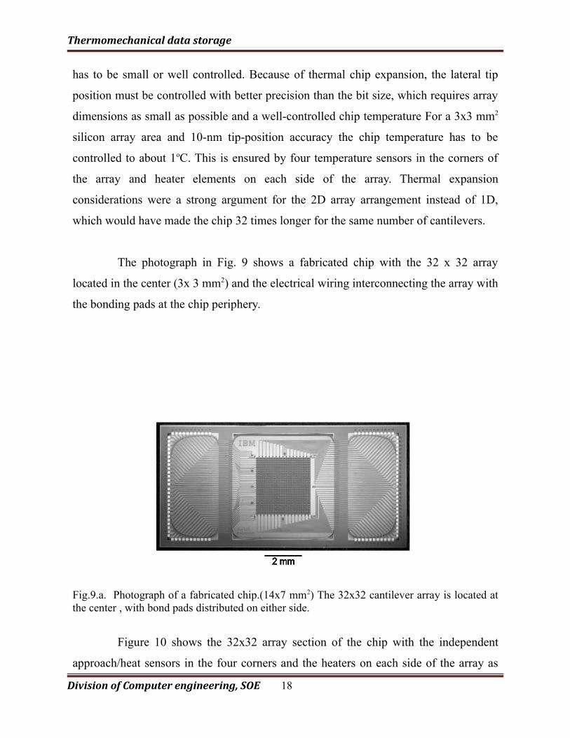
The photograph in Fig. 9 shows a fabricated chip with the 32 x 32 array
located in the center (3x 3 mm2) and the electrical wiring interconnecting the array with
the bonding pads at the chip periphery.
Fig.9.a. Photograph of a fabricated chip.(14x7 mm2) The 32x32 cantilever array is located at the center , with bond pads distributed on either side.
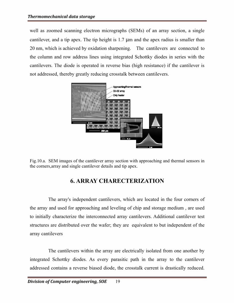
Figure 10 shows the 32x32 array section of the chip with the independent
approach/heat sensors in the four corners and the heaters on each side of the array as
Division of Computer engineering, SOE 18
Thermomechanical data storage
well as zoomed scanning electron micrographs (SEMs) of an array section, a single
cantilever, and a tip apex. The tip height is 1.7 µm and the apex radius is smaller than
20 nm, which is achieved by oxidation sharpening. The cantilevers are connected to
the column and row address lines using integrated Schottky diodes in series with the
cantilevers. The diode is operated in reverse bias (high resistance) if the cantilever is
not addressed, thereby greatly reducing crosstalk between cantilevers.
Fig.10.a. SEM images of the cantilever array section with approaching and thermal sensors in the corners,array and single cantilever details and tip apex.
6. ARRAY CHARECTERIZATION
The array's independent cantilevers, which are located in the four corners of
the array and used for approaching and leveling of chip and storage medium , are used
to initially characterize the interconnected array cantilevers. Additional cantilever test
structures are distributed over the wafer; they are equivalent to but independent of the
array cantilevers
The cantilevers within the array are electrically isolated from one another by
integrated Schottky diodes. As every parasitic path in the array to the cantilever
addressed contains a reverse biased diode, the crosstalk current is drastically reduced.
Division of Computer engineering, SOE 19
Thermomechanical data storage
Thus, the current response to an addressed cantilever in an array is nearly independent
of the size of the array. Hence, the power applied to address a cantilever is not shunted
by other cantilevers, and the reading sensitivity is not degraded-not even for very large
arrays (32 x32). The introduction electrical isolation using integrated Schottky diodes
turned out to be crucial for the successful operation of interconnected cantilever arrays
with a simple time-multiplexed addressing scheme.
The tip-apex height uniformity within an array is very important, because it
determines the force of each cantilever while in contact with the medium and hence
influences write/read performance as well as medium and tip wear. Wear investigations
suggest that a tip apex height uniformity across the chip of less than 500 nm is required
with the exact number depending on the spring constant of the cantilever. In the case of
the Millipede, the tip-apex height is determined by the tip height and the cantilever
bending.
7. THE POLYMER MEDIUM
The polymer storage medium plays a crucial role in Millipede like thermo-
mechanical storage systems. The thin-film-sandwich structure with PMMA as active
layer (see Fig. 1) is not the only choice possible, considering the almost unlimited
range of polymer materials available. The ideal medium should be easily deformable
for bit writing, yet written bits should be stable against tip wear and thermal
degradation. Finally, one would also like to be able to repeatedly erase and rewrite
bits .In order to be able to scientifically address all important aspects, some
understanding of the basic physical mechanism of thermomechanical bit writing and
erasing is required.
Division of Computer engineering, SOE 20
Thermomechanical data storage
In a gedanken experiment we visualize bit writing as the motion of a rigid
body, the tip, in a viscous medium, the polymer melt. For the time being, the polymer,
i.e.PMMA. is assumed to behave like a simple liquid after it has been treated above the
glass-transition temperature in a small volume around the tip. As viscous drag forces
must not exceed the loading force applied to the tip during indentation, we can estimate
an upper bound for the viscosity of the polymer melt using Stokes' equation
F = 6πηRυ (1)
In actual Millipede bit writing, the tip loading force is on the order F = 50 nN,
and the radius of curvature at the apex of the tip is typically R = 20 nm. Assuming a
depth of the indentation of, say, h = 50 nm and a heat pulse of τh=10µs duration, the
mean velocity during indentation is on the order of υ=h/τh=5mms-1 (note that thermal
relaxation times are of the order of microseconds ,and hence the heating time can be
equated to the time it takes to
form an indentation).With these parameters we obtain η< 25 Pa s, whereas typical
values for the shear viscosity of PMMA are at least 7 orders of magnitude larger even
at temperatures well above the glass-transition point.
This apparent contradiction can be resolved by considering that polymer
properties are strongly dependent on the time scale of observation. At time scales of the
order of 1ms and below, entanglement motion is in effect frozen in and the PMMA
molecules form a relatively static network. Deformation of the PMMA flow proceeds
by means of uncorrelated deformations of short molecular segments rather than by a
flow mechanism involving the coordinated motion of entire molecular chains. The
price one has to pay is that elastic stress builds up in the molecular network as a result
of the deformation (the polymer is in a so-called rubbery state). On the other hand,
corresponding relaxation times are orders of magnitude smaller1 giving rise to an
Division of Computer engineering, SOE 21
Thermomechanical data storage
effective viscosity at millipede time scales of the order of 10 Pa s as required by our
simple argument. [See Eq. (1)].Note that, unlike the normal viscosity, this high-
frequency viscosity is basically independent of the detailed molecular structure of the
PMMA, i.e. chain length, tacticity, poly dispersity, etc. In fact, we can even expect that
similar high-frequency viscous properties are found in a large class of other polymer
materials, which makes thermomechanical writing a rather robust process in terms of
material selection.
We have argued above that elastic stress builds up in the polymer film during
indentation, creating a corresponding reaction force on the tip of the order of Fr
=2πGR2, where G denotes the elastic shear modulus of the polymer. An important
property for Millipede operation is that the shear modulus drops by orders of
magnitude in the glass-transition regime, i.e. for PMMA from ~1 GPa below Tg to
~0.5... 1 MPa above Tg. (The bulk modulus, on the other hand, retains its low-
temperature value of several GPa. Hence, in
this elastic regime, formation of an indentation above 1; constitutes a volume
preserving deformation.) For proper bit writing, the tip load must be balanced between
the extremes of the elastic reaction force Fr for temperatures below and above Tg i.e. for
PMMA F « 2.5 1µN to prevent indentation of the polymer in the cold state and F»2.5
nN to overcome the elastic reaction force in the hot state. Unlike the deformation of a
simple liquid, the indentation represents a metastable state of the entire deformed
volume, which is under elastic tension. Recovery of the unstressed initial state is
prevented by rapid quenching of the indentation below the glass temperature with the
tip in place. As a result, the deformation is frozen in because below Tg motion of
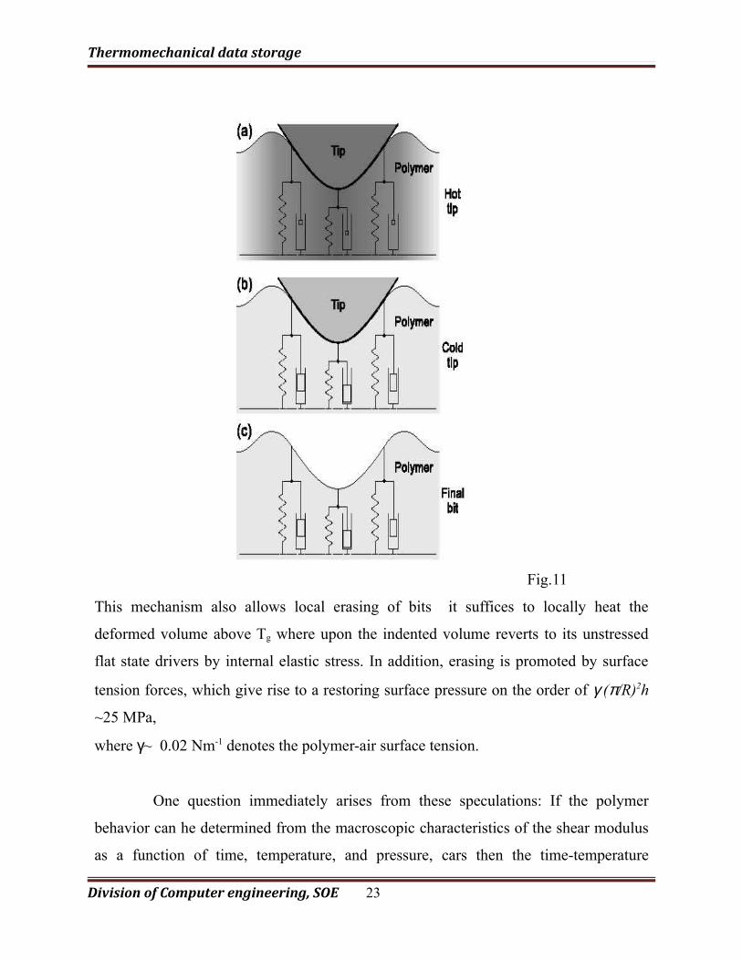
molecular-chain segments is effectively inhibited (see Figure 11).
Division of Computer engineering, SOE 22
Thermomechanical data storage
Fig.11
This mechanism also allows local erasing of bits it suffices to locally heat the
deformed volume above Tg where upon the indented volume reverts to its unstressed
flat state drivers by internal elastic stress. In addition, erasing is promoted by surface
tension forces, which give rise to a restoring surface pressure on the order of γ (π/R)2h
~25 MPa,
where γ~ 0.02 Nm-1 denotes the polymer-air surface tension.
One question immediately arises from these speculations: If the polymer
behavior can he determined from the macroscopic characteristics of the shear modulus
as a function of time, temperature, and pressure, cars then the time-temperature
Division of Computer engineering, SOE 23
Thermomechanical data storage
superposition principle also be applied in our case? The time temperature superposition
principle is a very successful concept of polymer physics .It basically says that the time
scale and the temperature are interdependent variables that determine the polymer
behavior such as the shear modulus. A simple transformation can be used to translate
time-dependent into temperature dependent data and vice versa. It is not clear,
however, whether this principle can be applied in our case. i.e. under such extreme
conditions (high pressures, short time scales and nanometer-sized volumes, which are
clearly below the radius of gyration of individual polymer molecules).
One of the most striking conclusions of our model of the bit-writing process is
that it should in principle work for most polymer materials. The general behavior of the
mechanical properties as a function of temperature and frequency is similar for all
polymers. The glass-transition temperature Tg would then be one of the main
parameters determining the threshold writing temperature.
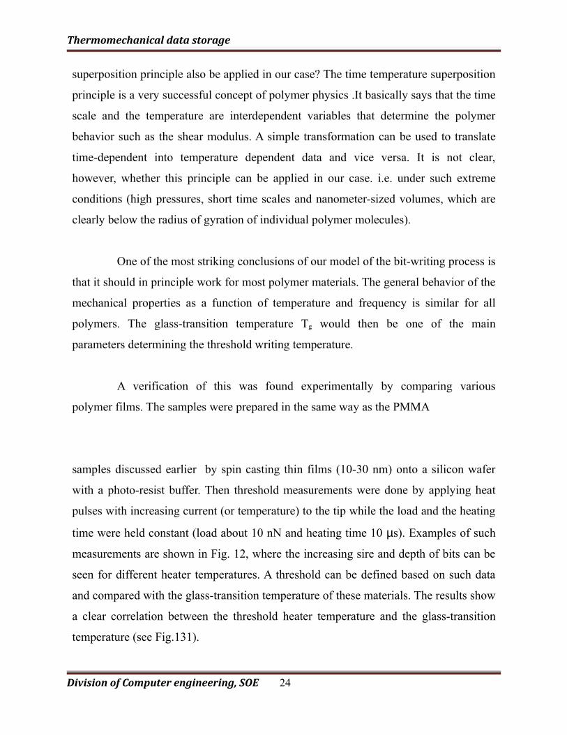
A verification of this was found experimentally by comparing various
polymer films. The samples were prepared in the same way as the PMMA
samples discussed earlier by spin casting thin films (10-30 nm) onto a silicon wafer
with a photo-resist buffer. Then threshold measurements were done by applying heat
pulses with increasing current (or temperature) to the tip while the load and the heating
time were held constant (load about 10 nN and heating time 10 µs). Examples of such
measurements are shown in Fig. 12, where the increasing sire and depth of bits can be
seen for different heater temperatures. A threshold can be defined based on such data
and compared with the glass-transition temperature of these materials. The results show
a clear correlation between the threshold heater temperature and the glass-transition
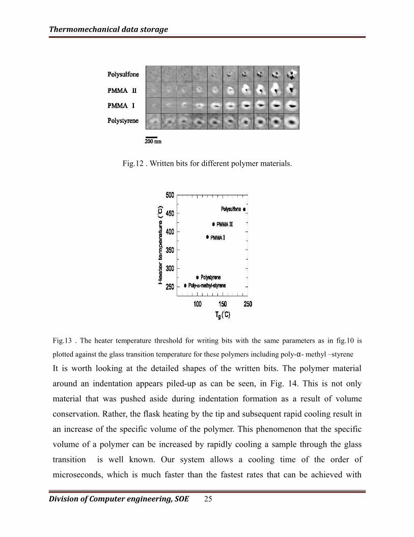
temperature (see Fig.131).
Division of Computer engineering, SOE 24
Thermomechanical data storage
Fig.12 . Written bits for different polymer materials.
Fig.13 . The heater temperature threshold for writing bits with the same parameters as in fig.10 is
plotted against the glass transition temperature for these polymers including poly-α- methyl –styrene
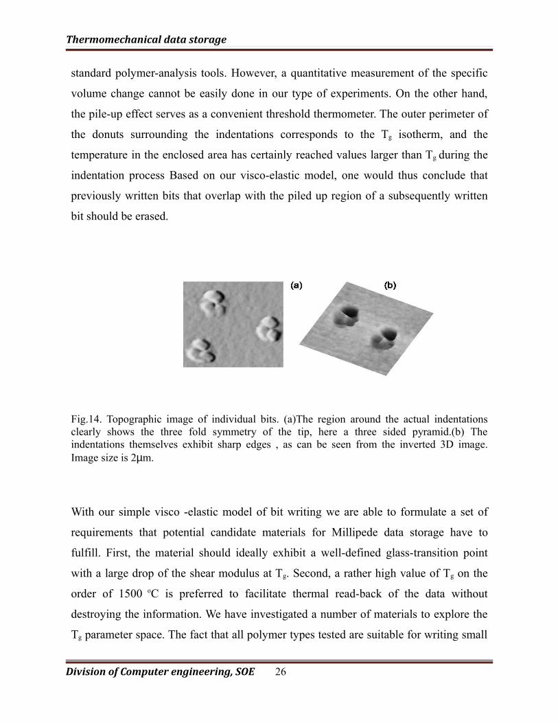
It is worth looking at the detailed shapes of the written bits. The polymer material
around an indentation appears piled-up as can be seen, in Fig. 14. This is not only
material that was pushed aside during indentation formation as a result of volume
conservation. Rather, the flask heating by the tip and subsequent rapid cooling result in
an increase of the specific volume of the polymer. This phenomenon that the specific
volume of a polymer can be increased by rapidly cooling a sample through the glass
transition is well known. Our system allows a cooling time of the order of
microseconds, which is much faster than the fastest rates that can be achieved with
Division of Computer engineering, SOE 25
Thermomechanical data storage
standard polymer-analysis tools. However, a quantitative measurement of the specific
volume change cannot be easily done in our type of experiments. On the other hand,
the pile-up effect serves as a convenient threshold thermometer. The outer perimeter of
the donuts surrounding the indentations corresponds to the Tg isotherm, and the
temperature in the enclosed area has certainly reached values larger than Tg during the
indentation process Based on our visco-elastic model, one would thus conclude that
previously written bits that overlap with the piled up region of a subsequently written
bit should be erased.
Fig.14. Topographic image of individual bits. (a)The region around the actual indentations clearly shows the three fold symmetry of the tip, here a three sided pyramid.(b) The indentations themselves exhibit sharp edges , as can be seen from the inverted 3D image. Image size is 2µm.
With our simple visco -elastic model of bit writing we are able to formulate a set of
requirements that potential candidate materials for Millipede data storage have to
fulfill. First, the material should ideally exhibit a well-defined glass-transition point
with a large drop of the shear modulus at Tg. Second, a rather high value of Tg on the
order of 1500 oC is preferred to facilitate thermal read-back of the data without
destroying the information. We have investigated a number of materials to explore the
Tg parameter space. The fact that all polymer types tested are suitable for writing small
Division of Computer engineering, SOE 26
Thermomechanical data storage
bits allows us to exercise the freedom of choice of polymer type to optimize in terms or
the technical requirements for a device, such as lifetime of bits, polymer endurance of
the read and write process, power consumption, etc. These are fields of ongoing,
research.
Based upon the pile-up effect, erasing of data bits may be explained.
8. DATA ERASING
The pile-up phenomenon turns out to be particularly beneficial for data-storage
applications. The following example demonstrates the effect. If we look at the sequence
of images in Fig. 15 taken on a standard PMMA sample, we find that the piled-up
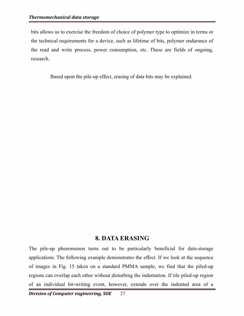
regions can overlap each other without disturbing the indentation. If tile piled-up region
of an individual bit-writing event, however, extends over the indented area of a
Division of Computer engineering, SOE 27
Thermomechanical data storage
previously written hit, tire depth of the corresponding indentation decreases markedly
(Fig. 15d).
This can he used for erasing written bits. However; if the pitch between two successive
bits is decreased even further, this erasing process will no longer work. Instead a broader
indentation is formed (Fig. 15d). Hence, to exclude mutual interference, the minimum
pitch between successive bits must be larger than the radius of the piled-up area around
an indentation.
Fig.15. Indentations in a PMMA film at several distances. The depth of the indentations is ~15 nm , about the thickness of the PMMA layer. The indentations on the left hand side werewritten first , then a second series of indentations were made decreasing distance to the first series in going from a to e.
In the example shown in Fig. 15 the temperature was chosen so high that the ring
around the indentations was very large, whereas the depth of the bit was limited by the
stop layer underneath the PMMA material. Clearly, here the temperature was too high
to form small bits, the minimum pitch being around 250 nm. However, by carefully
optimizing all parameters it is possible to achieve areal densities of up to 1Tb/in2 as
demonstrated in Fig. 2c.
Division of Computer engineering, SOE 28
Thermomechanical data storage
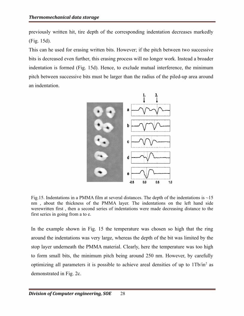
The new erasing scheme based on this volume effect switches from writing to
erasing merely by decreasing the pitch of writing indentations. This can, be done in, a
very controlled fashion as shown in Fig. 16, where individual lines or predefined sub-
areas are erased. Hence, this new erasing scheme can be made to work in a way that is
controlled on the scale of individual bits. Compared with earlier global erasing
schemes, this simplifies erasing significantly.
Fig.16 . Demonstration of the new erasing scheme.(a) A bit pattern with variable pitch in the vertical axis (fast scan axis) and constant pitch in the horizontal direction(slow scan axis) was prepared.(b) Then two of the lines were erased by decreasing the pitch in the vertical direction by a factor of three ,showing that the erasing scheme works for individual lines. One can also erase entire fields of bits without destroying bits at the edges of the fields. This is demonstrated in (c), where a field has been erased from a bit field similar to the one shown in (a0.The distance between the lines is 70nm
9. ADVANTAGES
The Advantages of this technology are :
1. Ultrahigh Density.
Division of Computer engineering, SOE 29
Thermomechanical data storage
2. Terabit Capacity.
3. Small Form Factor.
4. High Data Rates.
5. Not affected by electric or magnetic fields.
10. CONCLUSION
Day by day, the need for more storage capacity is going on increasing. Six or
seven years back, the maximum hard disk capacity available was about 2GB.But today
hard disks of 80 GB and 100GB are very common. The external size of the hard disk is
almost the same seven years back and today. It is the storage density that is being
Division of Computer engineering, SOE 30
Thermomechanical data storage
increased. After some years, the current method of magnetically storing data may reach
its limit of maximum achievable density. Beyond this super paramagnetic limit, the
capacity of magnetic storage cannot be increased. Hence there is a strong need for a
new storage technique. The Thermomechanical storage concept described above may
be considered as a good alternative. The millipede concept, which operates thousands
of cantilevers for write/read operation can provide ultra high storage capacity at very
high data rates. The Millipede project could bring tremendous data capacity to mobile
devices such as personal digital assistants, cellular phones, digital cameras and
multifunctional watches. In addition, the use of this concept may be explored in a
variety of other applications, such as large-area microscopic imaging, nanoscale
lithography or atomic and molecular manipulation. Research is going on to find new
storage mediums and to construct yet smaller cantilever tips , so that the storage
capacity can be increased further. In future we can expect a storage device of the size of
a button with storage capacity of trillions of bits.
11. REFERENCES
1. P.Vettiger,G.Cross,M.Despont,U.Drechsler,U.Durig,G.Gotsmann,W.Haberle,M.
A. Lantz,H.E.Routhuizen, R.Stutz,G.K.Binnig, IEEE Transactions in
Nanotechnology.1 (2002) 39-55
Division of Computer engineering, SOE 31
Thermomechanical data storage
2. E.Grochowski and R.F.Hoyt , "Future trends in hard disk drives ",IEEE
Transactions in Magnetics.vol 32,pp 1850-1854 (1996)
3. H.J.Mamin,R.D.Terris,L.S.Fan,S.Hoen,R.C.Barret, and D.Rugar, "High-density
data storage using proximal probe techniques ",IBM Journal of Research &
Development , vol 39 (1995)
4. www.ieee.org
5. www.research.ibm.com
6. www.zurich.ibm.com
7. www-snf.stanford.edu
8. www.almaden.ibm.com
9. www.physicsfinder.org
10. www.materialstoday.com
11.www.asrm.archivi.beniculturali.it/CFLR/Dobbiaco/Atti/Slides
12. www.me.gatech.edu/me/people/academic.faculty/King_William.html
13. www.domino.watson.ibm.com/Comm/bios.nsf/pages/afmdata.html
14. www.egr.msu.edu/~mackay/PDF%20Papers/2001-AppPhysLet-Millipede.pdf
15. www.nanoelectronicsplanet.com
16. www.sigmaxi.nsu.ru
17. www.moah.org
Division of Computer engineering, SOE 32
Thermomechanical data storage
Division of Computer engineering, SOE 33


![arXiv:1511.08755v1 [physics.ins-det] 25 Nov 2015 · 2015-11-30 · magnetic, thermomechanical and ferroelectric storage are listed in table I. Probe-based data storage has attracted](https://static.cupdf.com/doc/110x72/5e9270c3bcdada4afd742174/arxiv151108755v1-25-nov-2015-2015-11-30-magnetic-thermomechanical-and-ferroelectric.jpg)


![Thermomechanical Analysis [TMA] [NETZSCH]](https://static.cupdf.com/doc/110x72/55cf940b550346f57b9f3bd8/thermomechanical-analysis-tma-netzsch.jpg)