© KEMET Electronics Corporation • P.O. Box 5928 • Greenville, SC 29606 • 864-963-6300 • www.kemet.com C1039_KC-LINK_C0G • 4/6/2018 1One world. One KEMET
Surface Mount Multilayer Ceramic Chip Capacitors (SMD MLCCs)
KC-LINK™ for Fast Switching Semiconductor ApplicationsDC Link, Snubber, Resonator Capacitor, 150°C(Commercial & Automotive Grade)
Overview
KEMET's KC-LINK surface mount capacitors are designed to meet the growing demand for fast switching wide bandgap (WBG) semiconductors that operate at higher voltages, temperatures, and frequencies. By utilizing KEMET's robust and proprietary C0G/NPO base metal electrode (BME) dielectric system, these capacitors are well suited for power converters, inverters, snubbers, and resonators, where high efficiency is a primary concern. With extremely low effective series resistance (ESR) and very low thermal resistance, KC-LINK capacitors can operate at very high ripple currents with no change in capacitance versus DC voltage, and negligible change in capacitance versus temperature. With an operating temperature of 150°C, these capacitors can be mounted close to fast switching semiconductors in high power density applications, which require minimal cooling.
KC-LINK C0G dielectric technology also exhibits high mechanical robustness compared to other dielectric technologies, allowing the capacitor to be mounted without the use of lead frames. This provides extremely low effective series inductance (ESL) increasing the operating frequency range allowing for further miniaturization.
In addition to commercial grade, automotive grade devices are available and meet the demanding Automotive Electronics Council’s AEC–Q200 qualification requirements.
Benefits
• AEC-Q200 automotive qualified• Very high ripple current capability• Extremely low equivalent series resistance (ESR)• Extremely low equivalent series inductance (ESL)• Operating temperature range of −55°C to +150°C• High frequency operation (> 10 MHz)• No capacitance shift with voltage• No piezoelectric noise• High thermal stability• RoHS and Pb-free
Applications
• Wide bandgap (WBG), silicon carbide (SiC) and gallium nitride (GaN) systems
• EV/HEV (drive systems, charging)• Wireless charging• Photovoltaic systems• Power converters• Inverters• LLC resonant converters• DC link• Snubber

© KEMET Electronics Corporation • P.O. Box 5928 • Greenville, SC 29606 • 864-963-6300 • www.kemet.com C1039_KC-LINK_C0G • 4/6/2018 2
Surface Mount Multilayer Ceramic Chip Capacitors (SMD MLCCs)KC-LINK™ for Fast Switching Semiconductor Applications, DC Link, Snubber, Resonator Capacitor, 150°C (Commercial & Automotive)
Typical Performance - 3640, 220 nF, 500 VTypical Ripple Current (Arms)
1
Operating Voltage = 0 V Operating Voltage = 400 V
Frequency Typical ESR at 25°C
Typical ESL at 25°C RΘ
2 Ta = 105°C Ta = 125°C Ta = 105°C Ta = 125°C
50 kHz
< 4.0 mΩ 1 nH 15°C/W
20.6 15.4 8.6 8.6
100 kHz 19.3 14.4 17.1 14.4
200 kHz 17.9 13.4 17.9 13.4
300 kHz 17.2 12.8 17.2 12.8
1 Ta = Ambient temperature during ripple current measurements. Ripple current measurements performed with a peak capacitor temperature of 150°C. Samples mounted to heat sink with no forced air cooling.2 RΘ = Thermal resistance of KC-LINK 3640 224 nF 500 V capacitor.
0.00
0.01
0.10
1.00
10.00
100.00
10 100 1,000 10,000 100,000
Impe
danc
e (O
hms)
Frequency (kHz)
Impedance|Z|(Ohms) ESR (Ohms)
0.00
0.01
0.10
1.00
10 100 1,000 10,000 100,000
ESR
(Ohm
s)
Frequency (kHz)
ESR
Irms at Ta = 105°C Irms at Ta = 125°C
0
5
10
15
20
25
0 50 100 150 200 250 300 350
Ripp
le C
urre
nt (A
rms)
Frequency (kHz)
KC-LINK Ripple CurrentOperating Voltage: 400 VDC
−10
−5
0
5
10
−55 −35 −15 5 25 45 65 85 105 125 145
Capa
cita
nce
chan
ge (%
)
Temperature (°C)
Capacitance Change vs. Temperature
Capa
cita
nce
chan
ge (%
)
−10
−5
0
5
10
0 100 200 300 400 500DC Voltage (V)
Capacitance Change vs. DC Voltage
0
5
10
15
20
25
0 50 100 150 200 250 300 350
Ripp
le C
urre
nt (A
rms)
Frequency (kHz)
KC-LINK Ripple CurrentOperating Voltage: 0 VDC
Irms at Ta = 105°C Irms at Ta = 125°C

© KEMET Electronics Corporation • P.O. Box 5928 • Greenville, SC 29606 • 864-963-6300 • www.kemet.com C1039_KC-LINK_C0G • 4/6/2018 3
Surface Mount Multilayer Ceramic Chip Capacitors (SMD MLCCs)KC-LINK™ for Fast Switching Semiconductor Applications, DC Link, Snubber, Resonator Capacitor, 150°C (Commercial & Automotive)
Electrical Parameters/Characteristics
Item Parameters/CharacteristicsOperating temperature range −55°C to +150°C
Capacitance change with reference to +25°C and 0 VDC applied (TCC) ±30 PPM/°C
Aging rate (maximum % capacitance loss/decade hour) 0%
1Dielectric Withstanding Voltage (DWV) 750 VDC
2Dissipation Factor (DF) Maximum Limit at 25°C 0.1%
3Insulation Resistance (IR) Minimum Limit at 25°C 1,000 - MΩ - µF or 100 GΩ (500 VDC applied for 120 ±5 seconds at 25°C)
1 DWV is the voltage a capacitor can withstand (survive) for a short period of time. It exceeds the nominal and continuous working voltage of the capacitor.
2 Capacitance and dissipation factor (DF) measured under the following conditions: 1 MHz ±100 kHz and 1.0 ±0.2 Vrms if capacitance ≤ 1,000 pF 1 kHz ±50 Hz and 1.0 ±0.2 Vrms if capacitance > 1,000 pF3 To obtain IR limit, divide MΩ - µF value by the capacitance and compare to GΩ limit. Select the lower of the two limits.Note: When measuring capacitance it is important to ensure the set voltage level is held constant. The HP4284 and Agilent E4980 have a feature known as Automatic Level Control (ALC). The ALC feature should be switched to "ON."
Ordering InformationCKC 33 C 224 K C G A C TU
SeriesCase Size (L"x W")
Specification/ Series
Capacitance Code (pF)
Capacitance Tolerance
Rated Voltage (V)
DielectricSubclass
DesignationTermination
FinishPackaging
(Suffix/C-Spec)
CKC = KC-LINK
33 = 3640 C = Standard Two single digits and number of
zeros. Use 9 for
1.0 – 9.9 pF e.g., 2.2 pF
= 229
F = ±1%G = ±2%J = ±5%K = ±10%
C = 500 V G = C0G A = N/A C = 100% matte Sn See "Packaging
C-Spec Ordering Options Table" below
© KEMET Electronics Corporation • P.O. Box 5928 • Greenville, SC 29606 • 864-963-6300 • www.kemet.com C1039_KC-LINK_C0G • 4/6/2018 4
Surface Mount Multilayer Ceramic Chip Capacitors (SMD MLCCs)KC-LINK™ for Fast Switching Semiconductor Applications, DC Link, Snubber, Resonator Capacitor, 150°C (Commercial & Automotive)
Packaging C-Spec Ordering Options Table
Packaging Type Packaging/Grade Ordering Code (C-Spec)
Commercial Grade
7" Reel/Unmarked TU13" Reel (Embossed Plastic Tape)/
Unmarked 7210
Automotive Grade1
7" Reel AUTO13" Reel (Embossed Plastic Tape)/
Unmarked AUTO7210
1 For additional Information regarding "AUTO" C-Spec options, see "Automotive C-Spec Information."
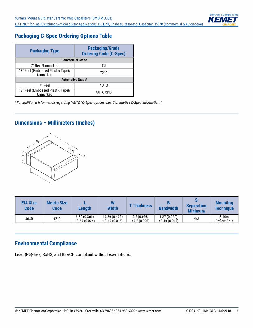
Dimensions – Millimeters (Inches)
L
B
W
S
T
EIA Size Code
Metric Size Code
L Length
W Width T Thickness B
Bandwidth
SSeparation Minimum
Mounting Technique
3640 9210 9.30 (0.366) ±0.60 (0.024)
10.20 (0.402) ±0.40 (0.016)
2.5 (0.098) ±0.2 (0.008)
1.27 (0.050) ±0.40 (0.016) N/A Solder
Reflow Only
Environmental Compliance
Lead (Pb)-free, RoHS, and REACH compliant without exemptions.
© KEMET Electronics Corporation • P.O. Box 5928 • Greenville, SC 29606 • 864-963-6300 • www.kemet.com C1039_KC-LINK_C0G • 4/6/2018 5
Surface Mount Multilayer Ceramic Chip Capacitors (SMD MLCCs)KC-LINK™ for Fast Switching Semiconductor Applications, DC Link, Snubber, Resonator Capacitor, 150°C (Commercial & Automotive)
Table 1 – Product Ordering Codes & Ratings
Capacitance Capacitance Code
Case Size 3640
Voltage Code C
Rated Voltage (VDC) 50
0
Capacitance Tolerance
220 nF 224 F G J K •
Table 2 – Performance & Reliability: Test Methods and Conditions (Commercial Only)
Stress Reference Test or Inspection MethodTerminal Strength JIS-C-6429 Appendix 1, Note: force of 1.8kg for 60 seconds.
Board Flex JIS-C-6429 Appendix 2, Note: 3.0 mm (minimum).
Solderability J-STD-002
Magnification 50X. Conditions:
a) Method B, 4 hours at 155°C, dry heat at 235°C
b) Method B at 215°C, category 3
c) Method D at 260°C, category 3
Temperature Cycling JESD22 Method JA-104 1,000 cycles (−55°C to +125°C), measurement at 24 hours ±4 hours after test conclusion.
Biased Humidity MIL-STD-202 Method 103
Load humidity: 1,000 hours 85°C/85% RH and 200 VDC maximum. Add 100 K ohm resistor. Measurement at 24 hours ±4 hours after test conclusion.Low volt humidity: 1,000 hours 85C°/85% RH and 1.5 V. Add 100 K ohm resistor. Measurement at 24 hours ±4 hours after test conclusion.
High Temperature Life MIL-STD-202 Method 108/EIA-198 1,000 hours at 150°C with 1.0 X rated voltage applied.
Storage Life MIL-STD-202 Method 108 150°C, 0 VDC, for 1,000 hours.
Vibration MIL-STD-202 Method 204
5 g's for 20 minutes, 12 cycles each of 3 orientations. Note: use 8" X 5" PCB 0.031" thick 7 secure points on one long side and 2 secure points at corners of opposite sides. Parts mounted within 2" from any secure point. Test from 10 – 2,000 Hz.
Mechanical Shock MIL-STD-202 Method 213 Figure 1 of Method 213, condition F.
Resistance to Solvents MIL-STD-202 Method 215 Add aqueous wash chemical, OKEM Clean or equivalent.
© KEMET Electronics Corporation • P.O. Box 5928 • Greenville, SC 29606 • 864-963-6300 • www.kemet.com C1039_KC-LINK_C0G • 4/6/2018 6
Surface Mount Multilayer Ceramic Chip Capacitors (SMD MLCCs)KC-LINK™ for Fast Switching Semiconductor Applications, DC Link, Snubber, Resonator Capacitor, 150°C (Commercial & Automotive)
Automotive C-Spec Information
The KEMET automotive grade products meet or exceed the requirements outlined by the Automotive Electronics Council. Details regarding test methods and conditions are referenced in document AEC–Q200, Stress Test Qualifi cation for Passive Components. These products are supported by a Product Change Notifi cation (PCN) and Production Part Approval Process warrant (PPAP).
Automotive products offered through our distribution channel have been assigned an inclusive ordering code C-Spec, “AUTO.” This C-Spec was developed in order to better serve small and medium-sized companies that prefer an automotive grade component without the requirement to submit a customer Source Controlled Drawing (SCD) or specifi cation for review by a KEMET engineering specialist. This C-Spec is therefore not intended for use by KEMET OEM automotive customers and are not granted the same “privileges” as other automotive C-Specs. Customer PCN approval and PPAP request levels are limited (see details below.)
Product Change Notifi cation (PCN)The KEMET Product Change Notifi cation system is used to communicate primarily the following types of changes: • Product/process changes that affect product form, fi t, function, and/or reliability • Changes in manufacturing site • Product obsolescence
KEMET Automotive C-Spec
Customer Notifi cation Due To: Days Prior To ImplementationProcess/Product change Obsolescence*
KEMET assigned1 Yes (with approval and sign off) Yes 180 days minimum
AUTO Yes (without approval) Yes 90 days minimum1 KEMET assigned C-Specs require the submittal of a customer SCD or customer specifi cation for review. For additional information contact KEMET.
Production Part Approval Process (PPAP)The purpose of the Production Part Approval Process is: • To ensure that supplier can meet the manufacturability and quality requirements for the purchased parts. • To provide the evidence that all customer engineering design records and specifi cation requirements are properly
understood and fulfi lled by the manufacturing organization. • To demonstrate that the established manufacturing process has the potential to produce the part.
KEMET Automotive C-Spec
PPAP (Product Part Approval Process) Level
1 2 3 4 5
KEMET assigned1 ● ● ● ● ●
AUTO ○ ○1 KEMET assigned C-Specs require the submittal of a customer SCD or customer specifi cation for review. For additional information contact KEMET.
● Part number specifi c PPAP available○ Product family PPAP only
© KEMET Electronics Corporation • P.O. Box 5928 • Greenville, SC 29606 • 864-963-6300 • www.kemet.com C1039_KC-LINK_C0G • 4/6/2018 7
Surface Mount Multilayer Ceramic Chip Capacitors (SMD MLCCs)KC-LINK™ for Fast Switching Semiconductor Applications, DC Link, Snubber, Resonator Capacitor, 150°C (Commercial & Automotive)
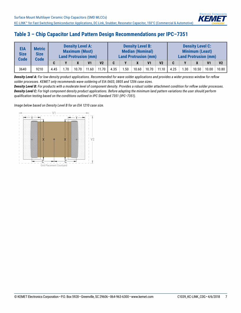
Table 3 – Chip Capacitor Land Pattern Design Recommendations per IPC–7351
EIA Size Code
Metric Size Code
Density Level A: Maximum (Most)
Land Protrusion (mm)
Density Level B: Median (Nominal)
Land Protrusion (mm)
Density Level C: Minimum (Least)
Land Protrusion (mm)C Y X V1 V2 C Y X V1 V2 C Y X V1 V2
3640 9210 4.45 1.70 10.70 11.60 11.70 4.35 1.50 10.60 10.70 11.10 4.25 1.30 10.50 10.00 10.80
Density Level A: For low-density product applications. Recommended for wave solder applications and provides a wider process window for reflow solder processes. KEMET only recommends wave soldering of EIA 0603, 0805 and 1206 case sizes.Density Level B: For products with a moderate level of component density. Provides a robust solder attachment condition for reflow solder processes.Density Level C: For high component density product applications. Before adapting the minimum land pattern variations the user should perform qualification testing based on the conditions outlined in IPC Standard 7351 (IPC–7351).
Image below based on Density Level B for an EIA 1210 case size.
Y
C C
X X
V1
V2
Grid Placement Courtyard
Y
© KEMET Electronics Corporation • P.O. Box 5928 • Greenville, SC 29606 • 864-963-6300 • www.kemet.com C1039_KC-LINK_C0G • 4/6/2018 8
Surface Mount Multilayer Ceramic Chip Capacitors (SMD MLCCs)KC-LINK™ for Fast Switching Semiconductor Applications, DC Link, Snubber, Resonator Capacitor, 150°C (Commercial & Automotive)
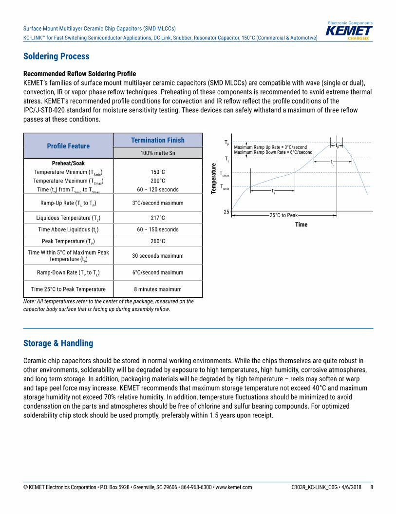
Soldering Process
Recommended Reflow Soldering ProfileKEMET’s families of surface mount multilayer ceramic capacitors (SMD MLCCs) are compatible with wave (single or dual), convection, IR or vapor phase reflow techniques. Preheating of these components is recommended to avoid extreme thermal stress. KEMET's recommended profile conditions for convection and IR reflow reflect the profile conditions of the IPC/J‐STD‐020 standard for moisture sensitivity testing. These devices can safely withstand a maximum of three reflow passes at these conditions.
Profile FeatureTermination Finish
100% matte Sn
Preheat/SoakTemperature Minimum (TSmin) 150°CTemperature Maximum (TSmax) 200°C
Time (tS) from TSmin to TSmax 60 – 120 seconds
Ramp-Up Rate (TL to TP) 3°C/second maximum
Liquidous Temperature (TL) 217°C
Time Above Liquidous (tL) 60 – 150 seconds
Peak Temperature (TP) 260°C
Time Within 5°C of Maximum Peak Temperature (tP) 30 seconds maximum
Ramp-Down Rate (TP to TL) 6°C/second maximum
Time 25°C to Peak Temperature 8 minutes maximum
Note: All temperatures refer to the center of the package, measured on the capacitor body surface that is facing up during assembly reflow.
Time
Tem
pera
ture
Tsmin
25
Tsmax
TL
TP Maximum Ramp Up Rate = 3°C/secondMaximum Ramp Down Rate = 6°C/second
tP
tL
ts
25°C to Peak
Storage & Handling
Ceramic chip capacitors should be stored in normal working environments. While the chips themselves are quite robust in other environments, solderability will be degraded by exposure to high temperatures, high humidity, corrosive atmospheres, and long term storage. In addition, packaging materials will be degraded by high temperature – reels may soften or warp and tape peel force may increase. KEMET recommends that maximum storage temperature not exceed 40°C and maximum storage humidity not exceed 70% relative humidity. In addition, temperature fluctuations should be minimized to avoid condensation on the parts and atmospheres should be free of chlorine and sulfur bearing compounds. For optimized solderability chip stock should be used promptly, preferably within 1.5 years upon receipt.
© KEMET Electronics Corporation • P.O. Box 5928 • Greenville, SC 29606 • 864-963-6300 • www.kemet.com C1039_KC-LINK_C0G • 4/6/2018 9
Surface Mount Multilayer Ceramic Chip Capacitors (SMD MLCCs)KC-LINK™ for Fast Switching Semiconductor Applications, DC Link, Snubber, Resonator Capacitor, 150°C (Commercial & Automotive)
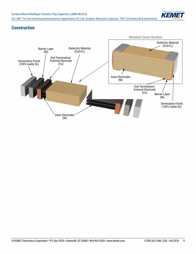
Construction
Detailed Cross Section
Barrier Layer(Ni)
Inner Electrodes(Ni)
Barrier Layer(Ni)
Inner Electrodes(Ni)
Dielectric Material(CaZrO3)Dielectric Material
(CaZrO3)
Termination Finish(100% matte Sn)
Termination Finish(100% matte Sn)
End Termination/External Electrode
(Cu)
End Termination/External Electrode
(Cu)

© KEMET Electronics Corporation • P.O. Box 5928 • Greenville, SC 29606 • 864-963-6300 • www.kemet.com C1039_KC-LINK_C0G • 4/6/2018 10
Surface Mount Multilayer Ceramic Chip Capacitors (SMD MLCCs)KC-LINK™ for Fast Switching Semiconductor Applications, DC Link, Snubber, Resonator Capacitor, 150°C (Commercial & Automotive)
Tape & Reel Packaging InformationKEMET offers multilayer ceramic chip capacitors packaged in 8, 12, 16 and 24 mm tape on 7" and 13" reels in accordance with EIA Standard 481. This packaging system is compatible with all tape-fed automatic pick and place systems. See Table 2 for details on reeling quantities for commercial chips.
8 mm, 12 mmor 16 mm carrier tape 178 mm (7.00")
or330 mm (13.00")
Anti-static reel
Embossed plastic* or punched paper carrier.
Embossment or punched cavity
Anti-static cover tape(0.10 mm (0.004") maximum thickness)
Chip and KPS orientation in pocket(except 1825 commercial, and 1825 and 2225 Military)
*EIA 01005, 0201, 0402 and 0603 case sizes available on punched paper carrier only.
KEMET®
Bar code label
Sprocket holes
Table 3 – Carrier Tape Confi guration, Embossed Plastic (mm)
EIA Case Size Tape Size (W)*
Embossed Plastic7" Reel 13" Reel
Pitch (P1)*
3640 24 16 16
*Refer to Figure 1 for W and P1 carrier tape reference locations.*Refer to Tables 4 and 5 for tolerance specifi cations.

© KEMET Electronics Corporation • P.O. Box 5928 • Greenville, SC 29606 • 864-963-6300 • www.kemet.com C1039_KC-LINK_C0G • 4/6/2018 11
Surface Mount Multilayer Ceramic Chip Capacitors (SMD MLCCs)KC-LINK™ for Fast Switching Semiconductor Applications, DC Link, Snubber, Resonator Capacitor, 150°C (Commercial & Automotive)
Figure 1 – Embossed (Plastic) Carrier Tape Dimensions
P0
T
F
W
Center Lines of Cavity
A0
B0
User Direction of Unreeling
Cover Tape
K0
B1 is for tape feeder reference only, including draft concentric about B0.
T2
ØD1
ØD0
B1
S1
T1
E1
E2
P1
P2
EmbossmentFor cavity size,see Note 1 Table 4
(10 pitches cumulativetolerance on tape ±0.2 mm)
Table 4 – Embossed (Plastic) Carrier Tape DimensionsMetric will govern
Constant Dimensions — Millimeters (Inches)
Tape Size D0 E1 P0 P2 R Reference
Note 2S1 Minimum
Note 3T
MaximumT1
Maximum
24 mm 1.5 +0.10/−0.0(0.059 +0.004/−0.0)
1.75 ±0.10(0.069 ±0.004)
4.0 ±0.10(0.157 ±0.004)
2.0 ±0.10(0.078 ±0.003)
30(1.181)
5(0.196)
0.250(0.009)
0.350(0.013)
Variable Dimensions — Millimeters (Inches)
Tape Size Pitch E2Minimum F P1
T2Maximum
WMaximum A0,B0 & K0
24 mm 16 mm 22.25(0.875)
11.5 ±0.10(0.452 ±0.003)
16.0 ±0.10(0.629 ±0.004)
3(0.118)
24.3(0.956)
1. The embossment hole location shall be measured from the sprocket hole controlling the location of the embossment. Dimensions of embossment location and hole location shall be applied independent of each other.
2. The tape with or without components shall pass around R without damage (see Figure 6).3. If S1 < 1.0 mm, there may not be enough area for cover tape to be properly applied (see EIA Document 481 paragraph 4.3 (b)).4. B1 dimension is a reference dimension for tape feeder clearance only.5. The cavity defi ned by A0, B0 and K0 shall surround the component with suffi cient clearance that:
(a) the component does not protrude above the top surface of the carrier tape.(b) the component can be removed from the cavity in a vertical direction without mechanical restriction, after the top cover tape has been removed.(c) rotation of the component is limited to 20° maximum for 8 and 12 mm tapes and 10° maximum for 16 mm tapes (see Figure 3).(d) lateral movement of the component is restricted to 0.5 mm maximum for 8 mm and 12 mm wide tape and to 1.0 mm maximum for 16 mm tape (see Figure 4)(e) For KPS Series product, A0 and B0 are measured on a plane 0.3 mm above the bottom of the pocket.(f) see Addendum in EIA Document 481 for standards relating to more precise taping requirements.

© KEMET Electronics Corporation • P.O. Box 5928 • Greenville, SC 29606 • 864-963-6300 • www.kemet.com C1039_KC-LINK_C0G • 4/6/2018 12
Surface Mount Multilayer Ceramic Chip Capacitors (SMD MLCCs)KC-LINK™ for Fast Switching Semiconductor Applications, DC Link, Snubber, Resonator Capacitor, 150°C (Commercial & Automotive)
Packaging Information Performance Notes
1. Cover Tape Break Force: 1.0 kg minimum.2. Cover Tape Peel Strength: The total peel strength of the cover tape from the carrier tape shall be:
Tape Width Peel Strength8 mm 0.1 to 1.0 Newton (10 to 100 gf)
12 and 16 mm 0.1 to 1.3 Newton (10 to 130 gf)
24 mm 0.1 to 1.6 Newton (10 to 160 gf)
The direction of the pull shall be opposite the direction of the carrier tape travel. The pull angle of the carrier tape shall be 165° to 180° from the plane of the carrier tape. During peeling, the carrier and/or cover tape shall be pulled at a velocity of 300±10 mm/minute.3. Labeling: Bar code labeling (standard or custom) shall be on the side of the reel opposite the sprocket holes. Refer to EIA Standards 556 and 624.
Figure 2 – Maximum Component Rotation
Ao
Bo
°T
°s
Maximum Component RotationTop View
Maximum Component RotationSide View
Tape MaximumWidth (mm) Rotation ( °
T)8,12 20 16 – 200 10 Tape Maximum
Width (mm) Rotation ( °S)
8,12 20 16 – 56 1072 – 200 5
Typical Pocket Centerline
Typical Component Centerline
Figure 3 – Maximum Lateral Movement
0.5 mm maximum0.5 mm maximum
8 mm & 12 mm Tape
1.0 mm maximum1.0 mm maximum
16 mm Tape
Figure 4 – Bending Radius
RRBending
Radius
EmbossedCarrier
PunchedCarrier
© KEMET Electronics Corporation • P.O. Box 5928 • Greenville, SC 29606 • 864-963-6300 • www.kemet.com C1039_KC-LINK_C0G • 4/6/2018 13
Surface Mount Multilayer Ceramic Chip Capacitors (SMD MLCCs)KC-LINK™ for Fast Switching Semiconductor Applications, DC Link, Snubber, Resonator Capacitor, 150°C (Commercial & Automotive)
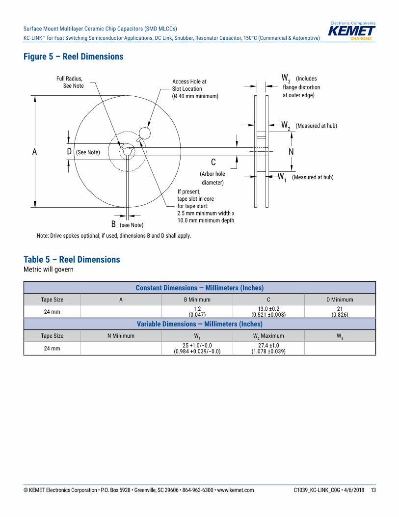
Figure 5 – Reel Dimensions
A D (See Note)
Full Radius,See Note
B (see Note)
Access Hole atSlot Location(Ø 40 mm minimum)
If present,tape slot in corefor tape start:2.5 mm minimum width x10.0 mm minimum depth
W3 (Includes flange distortion at outer edge)
W2 (Measured at hub)
W1 (Measured at hub)
C(Arbor holediameter)
Note: Drive spokes optional; if used, dimensions B and D shall apply.
N
Table 5 – Reel DimensionsMetric will govern
Constant Dimensions — Millimeters (Inches) Tape Size A B Minimum C D Minimum
24 mm 1.2(0.047)
13.0 ±0.2 (0.521 ±0.008)
21(0.826)
Variable Dimensions — Millimeters (Inches) Tape Size N Minimum W1 W2 Maximum W3
24 mm 25 +1.0/−0.0(0.984 +0.039/−0.0)
27.4 ±1.0(1.078 ±0.039)
© KEMET Electronics Corporation • P.O. Box 5928 • Greenville, SC 29606 • 864-963-6300 • www.kemet.com C1039_KC-LINK_C0G • 4/6/2018 14
Surface Mount Multilayer Ceramic Chip Capacitors (SMD MLCCs)KC-LINK™ for Fast Switching Semiconductor Applications, DC Link, Snubber, Resonator Capacitor, 150°C (Commercial & Automotive)
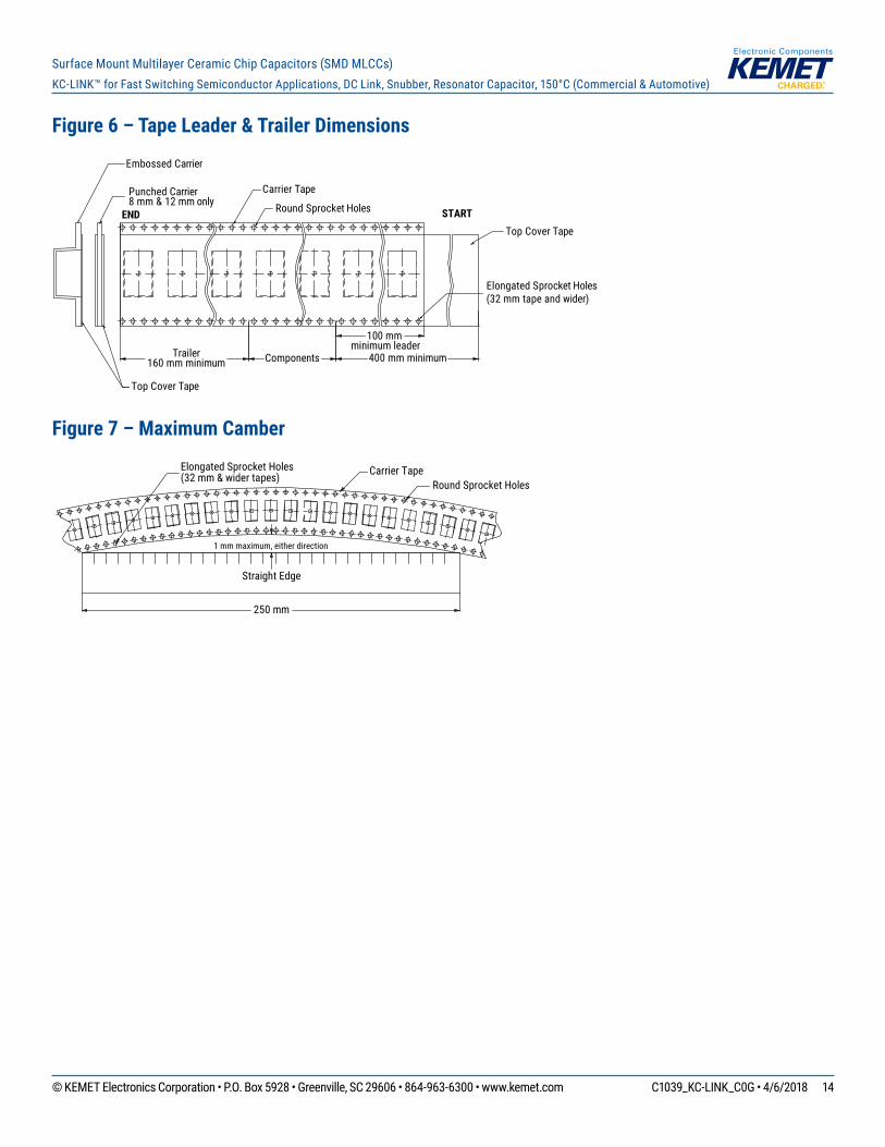
Figure 6 – Tape Leader & Trailer Dimensions
Trailer160 mm minimum
Carrier Tape
END STARTRound Sprocket Holes
Elongated Sprocket Holes(32 mm tape and wider)
Top Cover Tape
Top Cover Tape
Punched Carrier8 mm & 12 mm only
Embossed Carrier
Components
100 mm minimum leader
400 mm minimum
Figure 7 – Maximum Camber
Carrier TapeRound Sprocket Holes
1 mm maximum, either direction
Straight Edge
250 mm
Elongated Sprocket Holes(32 mm & wider tapes)
© KEMET Electronics Corporation • P.O. Box 5928 • Greenville, SC 29606 • 864-963-6300 • www.kemet.com C1039_KC-LINK_C0G • 4/6/2018 15
Surface Mount Multilayer Ceramic Chip Capacitors (SMD MLCCs)KC-LINK™ for Fast Switching Semiconductor Applications, DC Link, Snubber, Resonator Capacitor, 150°C (Commercial & Automotive)
KEMET Electronics Corporation Sales Offi ces
For a complete list of our global sales offi ces, please visit www.kemet.com/sales.
DisclaimerAll product specifi cations, statements, information and data (collectively, the “Information”) in this datasheet are subject to change. The customer is responsible for checking and verifying the extent to which the Information contained in this publication is applicable to an order at the time the order is placed.
All Information given herein is believed to be accurate and reliable, but it is presented without guarantee, warranty, or responsibility of any kind, expressed or implied.
Statements of suitability for certain applications are based on KEMET Electronics Corporation’s (“KEMET”) knowledge of typical operating conditions for such applications, but are not intended to constitute – and KEMET specifi cally disclaims – any warranty concerning suitability for a specifi c customer application or use. The Information is intended for use only by customers who have the requisite experience and capability to determine the correct products for their application. Any technical advice inferred from this Information or otherwise provided by KEMET with reference to the use of KEMET’s products is given gratis, and KEMET assumes no obligation or liability for the advice given or results obtained.
Although KEMET designs and manufactures its products to the most stringent quality and safety standards, given the current state of the art, isolated component failures may still occur. Accordingly, customer applications which require a high degree of reliability or safety should employ suitable designs or other safeguards (such as installation of protective circuitry or redundancies) in order to ensure that the failure of an electrical component does not result in a risk of personal injury or property damage.
Although all product–related warnings, cautions and notes must be observed, the customer should not assume that all safety measures are indicted or that other measures may not be required.
KEMET is a registered trademark of KEMET Electronics Corporation.