7/30/2019 Shiri Automatic
http://slidepdf.com/reader/full/shiri-automatic 1/55
MINOR PROJECT REPORT
ON
“AUTOMATIC PHASE CHANGER ”Submitted in the partial fulfillment of the requirement
For the award of the degree of
Bachelor of Technology
InElectronics & Communication Engineering
From
KURUKSHETRA UNIVERSITY, KURUKSHETRA
Guided By:
Miss. Priyanka Garg
(Lecturer,ECE)
Submitted To: Submitted By:
Mr. Jagtar Singh Krishan Malik(1507245)Ms. Rajni Meelu Sumit Kumar(1507246)
Anil Kumar (1508823)
Department of Electronics & Communication Engineering.
N. C. College of Engineering Israna (Panipat)
(July-Dec. 2010)
7/30/2019 Shiri Automatic
http://slidepdf.com/reader/full/shiri-automatic 2/55
CERTIFICATE
This is to certify that Project associates Mr. Krishan Malik(1507245), Mr. Sumit
Kumar(1507245) and Mr. Anil Kumar(1508823) of B.Tech. of VII semester,
Electronics & Communication Engineering,N.C college of engg., Israna(Panipat) have
successfully completed the minor project “AUTOMATIC PHASE CHANGER” under
my guidance.
They have worked sincerely with full dedication towards the successful completion of the
project.Wish them good luck for their bright future.
Dr. K.E. Hole Ms. Priyanka Garg
( HOD, ECE ) (Lecturer, ECE Dept.)
N.C.C.E. Israna, Panipat N.C.C.E. Israna, Panipat
7/30/2019 Shiri Automatic
http://slidepdf.com/reader/full/shiri-automatic 3/55
Acknowledgement
We are very happy on the completion of the Minor Project “AUTOMATIC PHASE
CHANGER ”. For this we would like to thank our Project guide “Ms. Priyanka Garg”
under whose visionary enlightenment we were able to complete this project.We would also like to acknowledge the help and support by Ms. Priyanka Garg who
spend his precious time.
Krishan Malik(1507245)
Sumit Kumar(1507246)
Anil Kumar(1508823)

7/30/2019 Shiri Automatic
http://slidepdf.com/reader/full/shiri-automatic 4/55
INDEXPg.no.
1. INTRODUCTION 5
2. COMPONENT LIST 6
3. COMPONENT DESCRIPTION 7-46
4. PCB MANUFACTURING 47
5. BLOCK DIAGRAM 48
6. CIRCUIT DIAGRAM 49
7. WORKING 50-51
8. PLANNING OF WORK 52
9. APLLICATIONS 53
10. BIBLOGRAPHY 54

7/30/2019 Shiri Automatic
http://slidepdf.com/reader/full/shiri-automatic 5/55
INTRODUCTION
Power instability in developing countries creates a need for automation of
electrical power generation or alternative sources of power to back up the
utility supply. This automation is required as the rate of power outage
becomes predominantly high. Most industrial and commercial processes aredependent on power supply and if the processes of change-over are manual,
serious time is not only wasted but also creates device or machine damage
from human error during the change-over connections, which could bring
massive losses.
The starting of the generator is done by a relay which switches the battery
voltage to ignition coil of the generator while the main power relay switches
the load to either public supply or generator. Fig 1 shows the general-ized
block diagram of the system. The approach used in this work is the modular
approach where the overall design was first broken into functional block
diagrams, where each block in the diagram represents a section of the circuit
that carries out a specific function. The functional block diagram of Fig. 1
also shows the interconnection between these blocks. Each section of the
block is analyzed below.
A manual change-over switch consists of a manual change-over switch
box, switch gear box and cut-out fuse or the connector fuse as described by
Rocks and Mazur (1993). This change-over switch box separate the source
between the generator and public supply, when there is power supply outage
from public supply, someone has to go and change the line to generator.
Thus when power supply is restored, someone has to put OFF the generator and then change the source line from generator to public supply.
In view of the above manual change-over switch system that involves
manpower by using ones energy in starting the generator and switching over
from public supply to generator and vice-versa when the supply is restored.
The importance attached to cases of operation in hospitals and air ports in
order to save life from generator as fast as possible makes it important for
7/30/2019 Shiri Automatic
http://slidepdf.com/reader/full/shiri-automatic 6/55
the design and construction of an automatic change-over switch which
would solve the problem of manpower and the danger likely to be
encountered changeover. The electronic control monitors the incoming
public supply voltage and detects when the voltage drops below a level that
electrical or electronics gadgets can function depending on the utility.
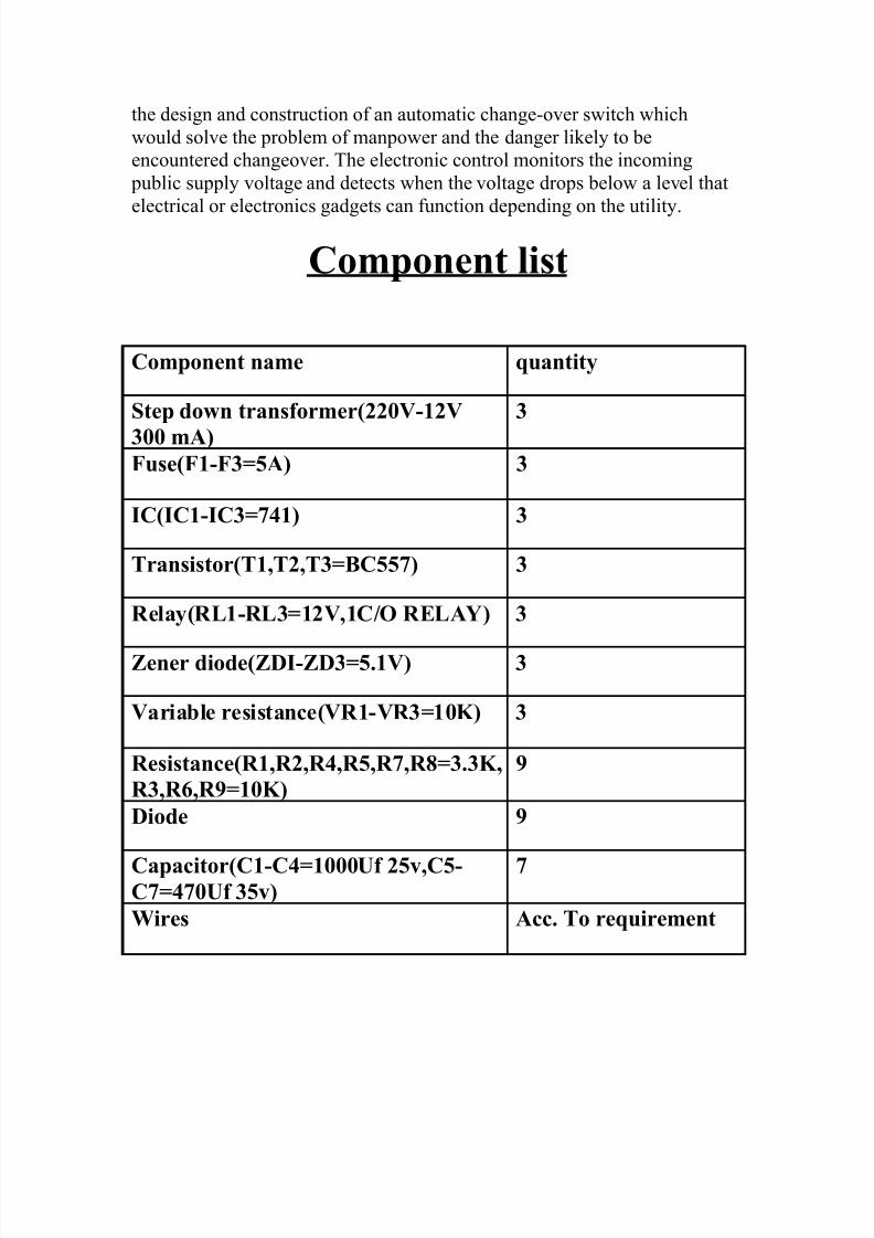
Component list
Component name quantity
Step down transformer(220V-12V
300 mA)
3
Fuse(F1-F3=5A) 3
IC(IC1-IC3=741) 3
Transistor(T1,T2,T3=BC557) 3
Relay(RL1-RL3=12V,1C/O RELAY) 3
Zener diode(ZDI-ZD3=5.1V) 3
Variable resistance(VR1-VR3=10K) 3
Resistance(R1,R2,R4,R5,R7,R8=3.3K,
R3,R6,R9=10K)
9
Diode 9
Capacitor(C1-C4=1000Uf 25v,C5-C7=470Uf 35v)
7
Wires Acc. To requirement

7/30/2019 Shiri Automatic
http://slidepdf.com/reader/full/shiri-automatic 7/55
COMPONENT DESCRIPTION
COMPARATOR
The IC 741 i.e. the operational amplifier is used as a comparator in the
circuit given above. As shown in the figure the IC 741 is a 8 pin IC in which
the pin no. 2 is known as the inverting terminal of the IC 741 because it is
connected to the negative potential.
The pin no. 3 is known as the non inverting terminal of the IC 741. The pin
no. 2 is connected to the reference voltage. The reference voltage is the
voltage which we set as a standard voltage in the circuit. The pin no. 2 is
connected to the input voltage. Now if we applied the input voltage to the IC

7/30/2019 Shiri Automatic
http://slidepdf.com/reader/full/shiri-automatic 8/55
741 then it will compare the input voltage to the reference voltage and if the
input voltage goes low then the output of the comparator is goes low. And if
the input voltage is equal to the reference voltage then the output of thecomparator is high.
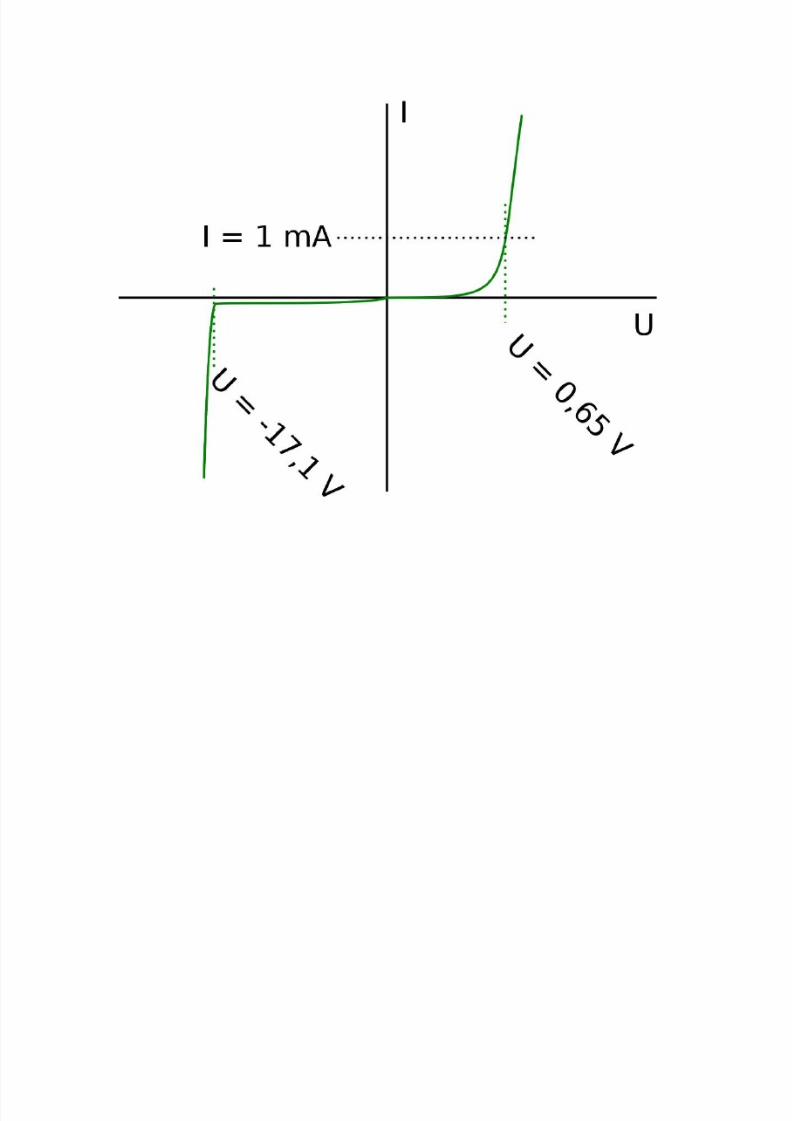
ZENER DIODE
A Zener diode is a type of diode
that permits current not only in the forward direction like a normal diode, but also in the reverse
direction if the voltage is larger than the breakdown voltage
Breakdown voltage
The breakdown voltage of an Insulator is the minimum voltage that causes a
portion of an insulator to become electrically conductive. The breakdown
voltage of a diode is the minimum reverse voltage to make the diode
conduct in reverse...

7/30/2019 Shiri Automatic
http://slidepdf.com/reader/full/shiri-automatic 9/55
known as "Zener knee voltage" or "Zener voltage". The device was named
after Clarence Zener
Clarence Zener
Clarence Melvin Zener was the American physicist who first described the
electrical property exploited by the Zener diode, which Bell Labs then
named after him...
, who discovered this electrical property.
A conventional solid-state diodeDiode
In electronics, a diode is a two-terminal electronic component that conducts
electric current in only one direction. The term usually refers to a
semiconductor diode, the most common type today. This is a crystalline
block of semiconductor material connected to two electrical terminals...
will not allow significant current if it is reverse-biased below its reverse
breakdown voltage. When the reverse bias breakdown voltage is exceeded, a
conventional diode is subject to high current due to avalanche breakdown.
Unless this current is limited by circuitry, the diode will be permanently
damaged. In case of large forward bias (current in the direction of the
arrow), the diode exhibits a voltage drop due to its junction built-in voltage
7/30/2019 Shiri Automatic
http://slidepdf.com/reader/full/shiri-automatic 10/55
and internal resistance. The amount of the voltage drop depends on the
semiconductor material and the doping concentrations.
A Zener diode exhibits almost the same properties, except the device is
specially designed so as to have a greatly reduced breakdown voltage, the
so-called Zener voltage. By contrast with the conventional device, a reverse-
biased Zener diode will exhibit a controlled breakdown and allow the current
to keep the voltage across the Zener diode at the Zener voltage. For example,
a diode with a Zener breakdown voltage of 3.2 V will exhibit a voltage drop
of 3.2 V if reverse bias voltage applied across it is more than its Zener
voltage. The Zener diode is therefore ideal for applications such as the
generation of a reference voltage (e.g. for an amplifier
Amplifier
Generally, an amplifier or simply amp, is any device that changes, usually
increases, the amplitude of a signal. The relationship of the input to theoutput of an amplifier—usually expressed as a function of the input
frequency—is called the transfer function of the amplifier, and the
magnitude of... stage, or as a voltage stabilizer for low-current applications.
The Zener diode's operation depends on the heavy doping
Doping (semiconductor)
In semiconductor production, doping is the process of intentionally
introducing impurities into an extremely pure semiconductor to change its
electrical properties. The impurities are dependent upon the type of semiconductor. Lightly and moderately doped semiconductors are referred
to as extrinsic...of its p-n junction
P-n junctionA p–n junction is formed by joining p-type and n-type semiconductors
together in very close contact. The term junction refers to the boundary
interface where the two regions of the semiconductor meet...allowing
electron
ElectronThe electron is a subatomic particle carrying a negative electric charge. It
has no known components or substructure, and therefore is believed to be an
elementary particle. An electron has a mass that is approximately 1/1836
that of the proton. The intrinsic angular momentum of the electron is as to
tunnel from the valence band of the p-type material to the conduction band
7/30/2019 Shiri Automatic
http://slidepdf.com/reader/full/shiri-automatic 11/55
of the n-type material. In the atomic scale, this tunneling corresponds to the
transport of valence band electrons into the empty conduction band states; as
a result of the reduced barrier between these bands and high electric fields
that are induced due to the relatively high levels of dopings on both sides.
The breakdown voltage can be controlled quite accurately in the doping
process. While tolerances within 0.05% are available, the most widely used
tolerances are 5% and 10%. Breakdown voltage for commonly available
zener diodes can vary widely from 1.2 volts to 200 volts.
Another mechanism that produces a similar effect is the avalanche effect as
in the avalanche diode
Avalanche diode
An avalanche diode is a diode that is designed to go through avalanche
breakdown at a specified reverse bias voltage and conduct as a type of
voltage reference..... The two types of diode are in fact constructed the sameway and both effects are present in diodes of this type. In silicon diodes up
to about 5.6 volts, the Zener effect is the predominant effect and shows a
marked negative temperature coefficient
. Above 5.6 volts, the avalanche effect
Avalanche breakdownAvalanche breakdown - is a phenomenon that can occur in both insulating
and semiconducting materials. It is a form of electric current multiplication
that can allow very large currents to flow within materials which are
otherwise good insulators. It is a type of electron avalanche.- Explanation... becomes predominant and exhibits a positive temperature coefficient. In a
5.6 V diode, the two effects occur together and their temperature coefficients
neatly cancel each other out, thus the 5.6 V diode is the component of choice
in temperature-critical applications. Modern manufacturing techniques have
produced devices with voltages lower than 5.6 V with negligible temperature
coefficients, but as higher voltage devices are encountered, the temperature
coefficient rises dramatically. A 75 V diode has 10 times the coefficient of a
12 V diode.
All such diodes, regardless of breakdown voltage, are usually marketedunder the umbrella term of "Zener diode".
7/30/2019 Shiri Automatic
http://slidepdf.com/reader/full/shiri-automatic 12/55

7/30/2019 Shiri Automatic
http://slidepdf.com/reader/full/shiri-automatic 13/55
DIODE
Symbol
Diode FunctionDiodes allow electricity to flow in only one direction. The arrow of the
circuit symbol shows the direction in which the current can flow. Diodes are
the electrical version of a valve and early diodes were actually called valves.
Forward Voltage DropElectricity uses up a little energy pushing its way through the diode, rather
like a person pushing through a door with a spring. This means that there is a
small voltage across a conducting diode, it is called the forward voltage drop
and is about 0.7V for all normal diodes which are made from silicon. The
forward voltage drop of a diode is almost constant whatever the current
passing through the diode so they have a very steep characteristic (current-
voltage graph).
Reverse VoltageWhen a reverse voltage is applied a perfect diode does not conduct, but all
real diodes leak a very tiny current of a few µA or less. This can be ignored
in most circuits because it will be very much smaller than the current
flowing in the forward direction. However, all diodes have a maximum
reverse voltage (usually 50V or more) and if this is exceeded the diode will fail
and pass a large current in the reverse direction, this is called breakdown.

7/30/2019 Shiri Automatic
http://slidepdf.com/reader/full/shiri-automatic 14/55
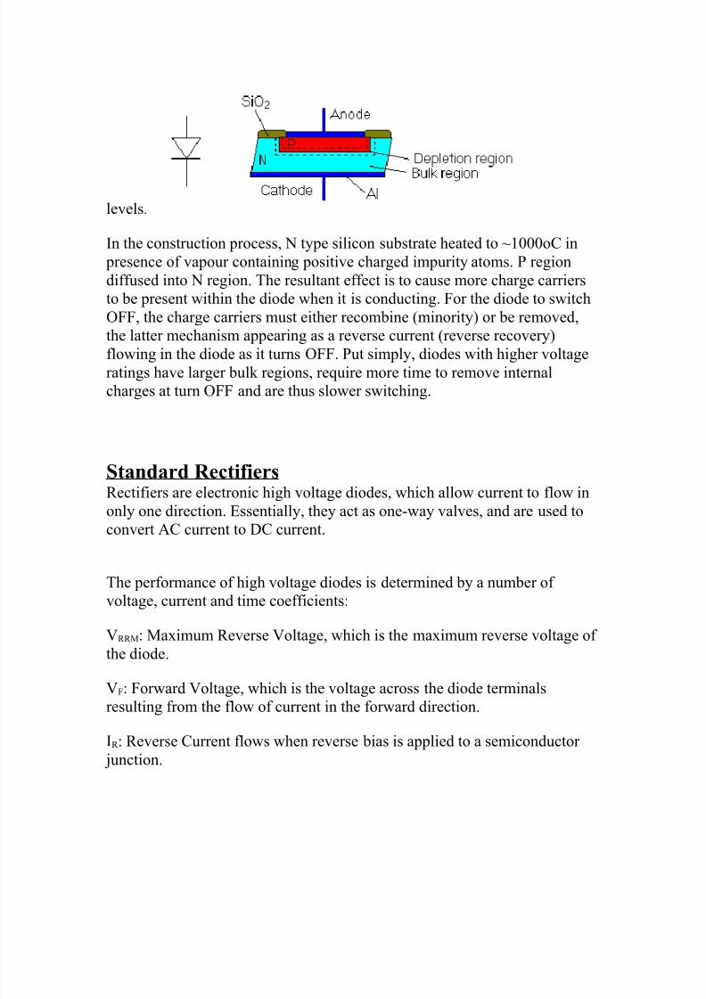
Diode ConstructionThe physical construction of a diode with a diffusion junction is shown in
the figure below. When a diode is reverse biased ie. a positive voltage is
applied to the cathode with respect to the anode, an electric field is formed
between the cathode and anode specifically across the depletion region. The
diode is 'reverse biased' and cannot conduct except for small leakagecurrents. However, if the electric field becomes too strong 'avalanche
breakdown' occurs and the diode will become a short circuit and often be
damaged. To counteract this the physical distance between the anode and
cathode is increased by increasing the size of the bulk region and changing
impurity atom doping
7/30/2019 Shiri Automatic
http://slidepdf.com/reader/full/shiri-automatic 15/55
levels.
In the construction process, N type silicon substrate heated to ~1000oC in
presence of vapour containing positive charged impurity atoms. P region
diffused into N region. The resultant effect is to cause more charge carriers
to be present within the diode when it is conducting. For the diode to switch
OFF, the charge carriers must either recombine (minority) or be removed,
the latter mechanism appearing as a reverse current (reverse recovery)
flowing in the diode as it turns OFF. Put simply, diodes with higher voltageratings have larger bulk regions, require more time to remove internal
charges at turn OFF and are thus slower switching.
Standard RectifiersRectifiers are electronic high voltage diodes, which allow current to flow in
only one direction. Essentially, they act as one-way valves, and are used to
convert AC current to DC current.
The performance of high voltage diodes is determined by a number of
voltage, current and time coefficients:
VRRM: Maximum Reverse Voltage, which is the maximum reverse voltage of
the diode.
VF: Forward Voltage, which is the voltage across the diode terminals
resulting from the flow of current in the forward direction.
IR : Reverse Current flows when reverse bias is applied to a semiconductor
junction.

7/30/2019 Shiri Automatic
http://slidepdf.com/reader/full/shiri-automatic 16/55
trr : Reverse Recovery Time is the time required for the current to reach a
specified reverse current (IR) after instantaneous switching from a specified
forward condition (IF).
IF: Forward Current is the current flowing through the diode in the direction
of lower resistance.
T j: Junction Operating Temperature is the range of temperatures in which the
high voltage diodes are designed to operate.
Fast RectifiersFigure 3a and b show typical styles of reverse recovery. The area within the
negative portion of each curve, , is the total reverse recovery charge Qrr
and represents the charge removal from the junction and the bulk regions of the
diode and is effectively independent of the forward current in the diode. The
recovery time t2 - t1 is dependant on the size of the bulk region thus high di/dt
currents can be obtained when using fast diodes. If the di/dt of the snap
recovery is too high and stray inductance exists in the circuit then extremely
high and possibly damaging voltage spikes can be induced.
(Note: ). Qrr can be found from manufacturers specifications thus the
maximum reverse recovery current Irr is given by:
If ta is very small compared to ta then ta trr and knowing the rate of decrease of
current di/dt = Irr/ta Irr/trr leads to:
Figure 3:
(a) Reverse recovery of a general purpose diode, (b) fast diode. Reverse
recovery time trr = t2 - t0.

7/30/2019 Shiri Automatic
http://slidepdf.com/reader/full/shiri-automatic 17/55
The effect of reverse recovery on the output voltage of a rectifier feeding a
resistive load is shown in figure 4.
Figure 4: Bridge rectifier output voltage showing diode reverse recovery
effects.
Ultra Fast RectifiersABSTRACT: International Rectifier's new series of Ultra-fast recoverydiodes are aimed specifically at the 12/24/48V SMPS output stage, and
extend the company's current product range of Ultra-fast recovery diodes
with industry standard part number products. The new product series has
been developed to meet today's requirement of high frequency operation and
power ratings, using a technology platform flexible enough to match the
performance improvement curve of the market requirements in the years to
come. The new IR Ultra-fast recovery diode series (200-400V) adopts
platinum diffusion in order to overcome the limitation of gold diffusion and
the electron irradiation technology. With this approach, the best trade off for leakage current, forward voltage drop and reverse recovery, has been
achieved with a maximum operating junction temperature of 175 degrees
Celsius and a reverse recovery time as low as 15-20ns. With this type of
performance, the maximum allowable switching frequency for this Ultra-
fast diode family would be up to 500-750kHz. This assumption is verified

7/30/2019 Shiri Automatic
http://slidepdf.com/reader/full/shiri-automatic 18/55
by the diode loss calculation used for the IR MUR1620 operating in a
typical output rectification in a forward converter.
7/30/2019 Shiri Automatic
http://slidepdf.com/reader/full/shiri-automatic 19/55
RELAY
OPERATING PRINCIPLES
There are really only two fundamentally different operatingprinciples: (1) electromagnetic attraction, and (2)electromagnetic induction. Electromagnetic attraction relaysoperate by virtue of a plunger being drawn into a solenoid,or an armature being attracted to the poles of anelectromagnet. Such relays may be actuated by d-c or by a-c
quantities.Electromagnetic-induction relays use the principle of theinduction motor whereby torqueis developed by induction in a rotor; this operating principleapplies only to relays actuated by alternating current, and indealing with those relays we shall call them simply"induction-type" relays.
DEFINITIONS OF OPERATION
Mechanical movement of the operating mechanism isimparted to a contact structure toclose or to open contacts. When we say that a relay"operates," we mean that it either closes or opens itscontacts-whichever is the required action under thecircumstances. Most relays have a "control spring," or arerestrained by gravity, so that they assume a given position
when completely de-energized; a contact that is closedunder this condition is called a "closed" contact, and onethat is open is called and "open" contact. This isstandardized nomenclature, but it can be quite confusingand awkward to use. A much better nomenclature in ratherextensive use is the designation ÒaÓ for an "open" contact,and ÒbÓ for a "closed" contact. This nomenclature will be

7/30/2019 Shiri Automatic
http://slidepdf.com/reader/full/shiri-automatic 20/55
used in this book. The present standard method for showing"a" and ÒbÓ contacts on connection diagrams is illustratedin Fig. 1. Even though an ÒaÓ contact may be closed undernormal operating conditions, it should be shown open as in
Fig. 1; and similarly,even though a ÒbÓ contact may normally be open, it shouldbe shown closed.When a relay operates to open a ÒbÓ contact or to close anÒaÓ contact, we say that it "picks up," and the smallestvalue of the actuating quantity that will cause suchoperation, as the quantity is slowly increased from zero, iscalled the "pickup" value. When a relay operates to close aÒbÓ contact, or to move to a stop in place of a ÒbÓ contact,we say that it "resets"; and the largest value of the actuating
quantity at which this occurs, as the quantity is slowly
decreased from above the pickup value, is called the "reset"value. When a relay operates to open its ÒaÓ contact, butdoes not reset, we say that it "drops out," and the largestvalue of the actuating quantity at which this occurs is calledthe "drop-out" value.
7/30/2019 Shiri Automatic
http://slidepdf.com/reader/full/shiri-automatic 21/55
TRANSFORMER
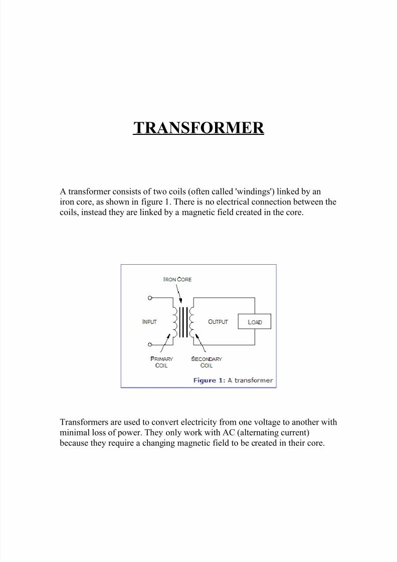
A transformer consists of two coils (often called 'windings') linked by an
iron core, as shown in figure 1. There is no electrical connection between the
coils, instead they are linked by a magnetic field created in the core.
Transformers are used to convert electricity from one voltage to another with
minimal loss of power. They only work with AC (alternating current)
because they require a changing magnetic field to be created in their core.

7/30/2019 Shiri Automatic
http://slidepdf.com/reader/full/shiri-automatic 22/55
Transformers can increase voltage (step-up) as well as reduce voltage (step-
down).
Alternating current flowing in the primary (input) coil creates a continually
changing magnetic field in the iron core. This field also passes through the
secondary (output) coil and the changing strength of the magnetic field
induces an alternating voltage in the secondary coil. If the secondary coil is
connected to a load the induced voltage will make an induced current flow.
The correct term for the induced voltage is 'induced electromotive force'
which is usually abbreviated to induced e.m.f.
The iron core is laminated to prevent 'eddy currents' flowing in the core.
These are currents produced by the alternating magnetic field inducing a
small voltage in the core, just like that induced in the secondary coil. Eddy
currents waste power by needlessly heating up the core but they are reducedto a negligible amount by laminating the iron because this increases the
electrical resistance of the core without affecting its magnetic properties.
Transformers have two great advantages over other methods of changing
voltage:
1. They provide total electrical isolation between the input and output, so
they can be safely used to reduce the high voltage of the mains supply.
2. Almost no power is wasted in a transformer. They have a high
efficiency (power out / power in) of 95% or more.
Mains transformers are the most common type. They are designed to reduce
the AC mains supply voltage (230-240V in the UK or 115-120V in some
countries) to a safer low voltage. The standard mains supply voltages are
officially 115V and 230V, but 120V and 240V are the values usually quoted
and the difference is of no significance in most cases.

7/30/2019 Shiri Automatic
http://slidepdf.com/reader/full/shiri-automatic 23/55
To allow for the two supply voltages mains transformers usually have two
separate primary coils (windings) labelled 0-120V and 0-120V. The two
coils are connected in series for 240V (figure 2a) and in parallel for 120V
(figure 2b). They must be wired the correct way round as shown in the
diagrams because the coils must be connected in the correct sense
(direction):
Most mains transformers have two separate secondary coils (e.g. labelled 0-
9V, 0-9V) which may be used separately to give two independent supplies,
or connected in series to create a centre-tapped coil (see below) or one coil
with double the voltage.
Some mains transformers have a centre-tap halfway through the secondary
coil and they are labelled 9-0-9V for example. They can be used to producefull-wave rectified DC with just two diodes, unlike a standard secondary coil
which requires four diodes to produce full-wave rectified DC.
A mains transformer is specified by:
1. Its secondary (output) voltages Vs.

7/30/2019 Shiri Automatic
http://slidepdf.com/reader/full/shiri-automatic 24/55
2. Its maximum power, Pmax, which the transformer can pass, quoted in
VA (volt-amp). This determines the maximum output (secondary)
current, Imax...
...where Vs is the secondary voltage. If there are two secondary coils
the maximum power should be halved to give the maximum for each
coil.
3. Its construction - it may be PCB-mounting, chassis mounting (with
solder tag connections) or toroidal (a high quality design).
STEP DOWN TRANSFORMER
If the first coil has more turns that the second coil, the secondary voltage is
smaller than the primary voltage:
This is called a step-down transformer. If the second coil has half as many
turns as the first coil, the secondary voltage will be half the size of the

7/30/2019 Shiri Automatic
http://slidepdf.com/reader/full/shiri-automatic 25/55
primary voltage; if the second coil has one tenth as many turns, it has one
tenth the voltage. In general:
Secondary voltage ÷ Primary voltage = Number of turns in secondary ÷
Number of turns in primary
The current is transformed the opposite way—increased in size—in a step-
down transformer:
Secondary current ÷ Primary current = Number of turns in primary ÷
Number of turns in secondary
So a step-down transformer with 100 coils in the primary and 10 coils in the
secondary will reduce the voltage by a factor of 10 but multiply the current
by a factor of 10 at the same time. The power in an electric current is equal
to the current times the voltage (watts = volts x amps is one way to
remember this), so you can see the power in the secondary coil is
theoretically the same as the power in the primary coil. (In reality, there is
some loss of power between the primary and the secondary because some of
the "magnetic flux" leaks out of the core, some energy is lost because the
core heats up, and so on.)

7/30/2019 Shiri Automatic
http://slidepdf.com/reader/full/shiri-automatic 26/55
CAPACITOR
FUNDAMENTALS FOR ALL CAPACITORS
This bulletin describes the basic characteristics of KEMET capacitors.
Before examining all the details relating to KEMET products, here are some
of the basics of all capacitors and then
of the major types sold under the KEMET brands: solid tantalum
and monolithic ceramic.
For all practical purposes, consider only the parallel-plate capacitor:
two conductors or electrodes separated by a dielectric
material of uniform thickness. The conductors can be any material
which will conduct electricity easily. The dielectric material
must be a poor conductor – an insulator.

7/30/2019 Shiri Automatic
http://slidepdf.com/reader/full/shiri-automatic 27/55
The symbol for a capacitor used in schematic diagrams of electronic
circuits looks very much like a parallel-plate model.
7/30/2019 Shiri Automatic
http://slidepdf.com/reader/full/shiri-automatic 28/55
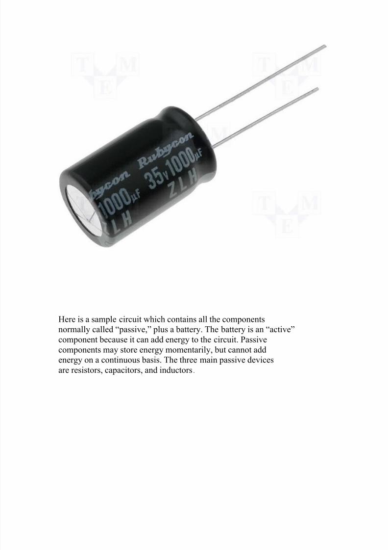
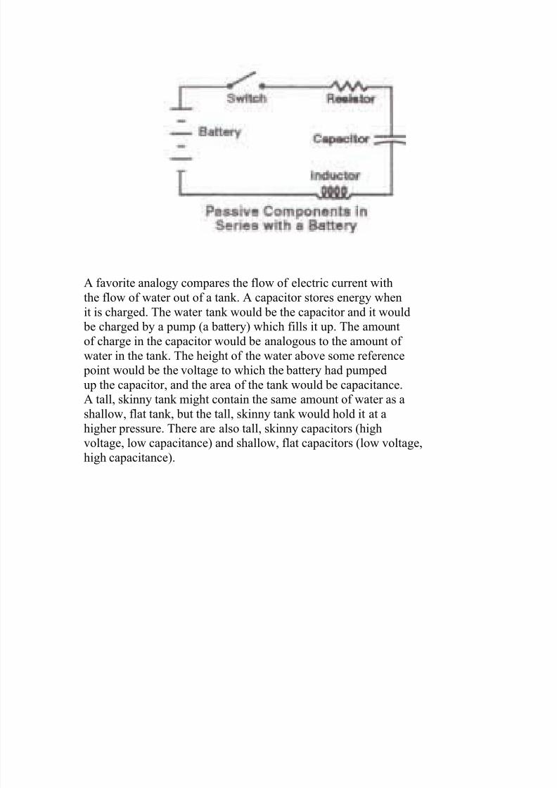
Here is a sample circuit which contains all the components
normally called “passive,” plus a battery. The battery is an “active”
component because it can add energy to the circuit. Passive
components may store energy momentarily, but cannot add
energy on a continuous basis. The three main passive devices
are resistors, capacitors, and inductors.
7/30/2019 Shiri Automatic
http://slidepdf.com/reader/full/shiri-automatic 29/55
A favorite analogy compares the flow of electric current with
the flow of water out of a tank. A capacitor stores energy when
it is charged. The water tank would be the capacitor and it would
be charged by a pump (a battery) which fills it up. The amount
of charge in the capacitor would be analogous to the amount of
water in the tank. The height of the water above some reference
point would be the voltage to which the battery had pumped
up the capacitor, and the area of the tank would be capacitance.
A tall, skinny tank might contain the same amount of water as a
shallow, flat tank, but the tall, skinny tank would hold it at ahigher pressure. There are also tall, skinny capacitors (high
voltage, low capacitance) and shallow, flat capacitors (low voltage,
high capacitance).

7/30/2019 Shiri Automatic
http://slidepdf.com/reader/full/shiri-automatic 30/55
There is also a pipe coming out of the tank and a valve. If the
valve is open, water runs out. The valve is both a switch and a
resistor. If the valve is opened only partially, it causes enough
friction so that water runs slowly from the tank. It behaves like
a variable resistor. When resistance is high, the water runs
slowly, but if resistance is made small, the water can run more
freely. Once the water is running, it can be stopped by closing
the valve. The water in the pipe, already in motion, must stop.If the valve is closed very quickly, then the water must stop
flowing very quickly. Water “hammers” in some plumbing systems
which causes a distant “clunk” when a valve is closed
quickly. The energy in the moving water suddenly has no place
to go, so it bangs a pipe against its support somewhere.
The moving water has acted like the inductor acts in the electronic
circuit. The battery is the pump, the capacitor is the
tank, the resistor and the switch are the valve, and the inductor
is the moving water in the pipe.

7/30/2019 Shiri Automatic
http://slidepdf.com/reader/full/shiri-automatic 31/55
What happens inside a capacitor? When charged by a battery,
one electrode of the capacitor will become positively chargedand the other one will be correspondingly negatively charged.
When the diagram of the capacitor is magnified, it can be seen
that the presence of electrical charges on the electrodes induces
charges in the dielectric. These induced charges determine
something called permittivity. Each different dielectric material
has its own value of permittivity. A more practical and better
known measurement tool is called “K,” or dielectric constant.
“K” is the ratio of the permittivity of the dielectric in use

7/30/2019 Shiri Automatic
http://slidepdf.com/reader/full/shiri-automatic 32/55
to the permittivity of free space – a vacuum. Therefore, all the
capacitance values are related to the permittivity of vacuum.
.In a vacuum, K = 1, while “K” in every material has some value
greater than 1. The higher the “K,” the more capacitance can
be realized, with all other things being equal.
The expression of capacitance is seen here, and note the presence
of the constant, 8.85 X 10⁻¹² (permittivity of vacuum).

7/30/2019 Shiri Automatic
http://slidepdf.com/reader/full/shiri-automatic 33/55
The only trick involved in using this equation is to keep the units consistent.
Capacitance is in farads, the area “A” is in square meters and the distance
between electrodes “D” is in meters. “K” is a ratio and a pure number
without dimensions.
Sometimes different constants are used in the equation. This comes about
when units other than farads and meters are used. Microfarads and inches
might be used, for example.
To get an idea of what a farad is, calculate the area which would be
necessary in a capacitor built to have one farad, to operate in a vacuum, and
to have a spacing between electrodes of one millimeter. First, turn the
equation around to solve for the area and then plug in the values known.
This calculates to 113 million square meters, which would be a field about
6.5 miles on a side. It’s not hard to see why one farad capacitors aren’t made
very often and when they are, they are never made with a vacuum dielectricand a one millimeter spacing. Vacuum capacitors are made, but the market is
pretty well limited to laboratory standards.
All commercial capacitors use some different dielectric
material with a higher value of K.
Materials
C = (8.85 X 10 -12) K ADor A =(8.85 X 10 -12) KCDGiven: K = 1C = 1 faradD = 1 millimeter (or 0.001 meters)A = 1 x 0.001 = 113,000,000 sq. meters(8.85 X 10 -12) x 1

7/30/2019 Shiri Automatic
http://slidepdf.com/reader/full/shiri-automatic 34/55
FUSE
An electrical fuse is a current interrupting device which protects an electrical
circuit in which it is installed by creating an open circuit condition inresponse to excessive current. The current is interrupted when the element or
elements which carry the current are melted by heat generated by the
current. Fuse terminals typically form an electrical connection between an
electrical power source and an electrical component or a combination of
components arranged in an electrical circuit. A fusible link is connected
between the fuse terminals, so that when electrical current flowing through
the fuse exceeds a predetermined limit, the fusible link melts and opens the
circuit through the fuse to prevent electrical component damage.
A standard fuse is a one time use device that must be replaced after an
overload condition has been cleared because the thin strip or ribbon of metalcannot be rejoined after it has melted through. Over-current protection may
be provided by fuses as well as by circuit breakers, switches, relays and
other devices. Each type of equipment has variations in ratings, service
requirements and costs. Fuses generally present the most cost-effective
means for providing automatic high-voltage current protection against a
single over-current failure. Most types of fuses are designed to minimize
damage to conductors and insulation from excessive current. Fuses are
employed in many electrical systems that are used by people on an everyday
basis. For example, fuses are part of electrical systems found inautomobiles, boats, motorcycles and other vehicles. These fuses function to
stop electricity from flowing to a particular component of the system by
creating an open circuit as a result of an unsafe electrical condition.
Fuses are typically employed in the electrical utility industry to protect
distribution transformers, cables, capacitor banks and other equipment from
damaging overcurrents. The fuses are arranged to disconnect the faulted

7/30/2019 Shiri Automatic
http://slidepdf.com/reader/full/shiri-automatic 35/55
equipment or circuit promptly from its source of supply before damage can
occur. Fuses are used extensively in high voltage electrical networks in order
to protect the electrical equipment in the network from damage caused
by surges through the system, generally occasioned by short-circuits or
overloads. Fuses are used as necessary to protect semiconductors. Safety
fuses that basically can be electrically connected in series with the
semiconductor power elements require special installation space and the
construction expense that goes along with it. They add electrical series
resistance, which results in current-dependent heat loss.
Fuses are very important in protecting circuitry from overload conditions.
Fuses are devices which, by melting of one or more of their parts intended
and designed for this purpose, open the circuit by interrupting the current if
the current exceeds a predetermined value for a sufficiently long period of
time. They are designed to blow open at predetermined current levels and
are selected based upon safety specifications designated for a particular circuit.
The fusible element or fuse link is intended to melt away under the influence
of a current which exceeds a particular value for a particular length of time.
There are thermal fuses, mechanical fuses, spark gap surge arrestors,
varistors, and other similar devices, each designed specifically as a solution
to one or more extreme electrical events. Each device provides benefit in

7/30/2019 Shiri Automatic
http://slidepdf.com/reader/full/shiri-automatic 36/55
particular situations that may be greater than other types of devices. In
general, an electrical fuse combines both a sensing and interrupting element
in one self-contained device and is direct acting in that it responds only to a
combination of magnitude and duration of current flowing through it. The
fuse normally does not include any provision for making or breaking the
connection to an energized circuit but requires separate devices
to perform this function.
A fuse is a single-phase device, such that only the fuse in the phase or
phases subjected to overcurrent will respond to de-energize the affected
phase or phases of the circuit that is faulty. After having interrupted
an overcurrent, it is replaced to restore service. Currently, two basic types of
fuses are employed, the expulsion fuse and the current limiting fuse. Each
type employs a fusible element designed to melt when a current of a
predetermined magnitude and duration passes through the element. The
expulsion type fuse interrupts overcurrents through the deionizing action of gases that are liberated when the fusible element melts. An expulsion fuse
typically employs a relatively short length of a fusible element contained
within a tubular enclosure that is part of a larger assembly known as a
fuseholder. The enclosure used in the expulsion type fuse is lined with an
organic material. Interruption of an overcurrent takes place within the fuse
by the deionizing and explosive action of the gases which are liberated
when the liner is exposed to the heat of the arc that is created when the
fusible element melts in response to the overcurrent. The operation of the
expulsion-type fuse is characterized by loud noise and violent emission of
gases, flame and burning debris, all of which pose a danger to personnel who
may be in close proximity to the fuse when it operates. Because of its violent
mode of operation, this type of fuse has generally been restricted to outdoor
usage only. The current-limiting type interrupts overcurrents when the arc
that is established by the melting of the fusible element is subjected to the
mechanical restriction and cooling action of a sand filler that surrounds the
fusible element.
A current-limiting fuse typically consists of one or more silver wire or
ribbon elements of a required length which are electrically connected at their
ends to a pair of electrical terminations. The assembly is placed in a tubular housing that is made of a highly temperature-resistant
material, and the housing is then typically filled with high-purity silica sand
and sealed.
Electrical fuses have taken many forms and generally comprise fuses having
a fusible link extending between a pair of terminal portions.

7/30/2019 Shiri Automatic
http://slidepdf.com/reader/full/shiri-automatic 37/55
7/30/2019 Shiri Automatic
http://slidepdf.com/reader/full/shiri-automatic 38/55
in various devices having a low electrical power of less than 1A. For
example, such a fuse is suitable for fuse-matching in a wire harness
composed of wires having a small diameter, and which connects a series of
electronic elements in a car. In such fields, utilization of card type fuses has
been increasing.
Solid state fuses are also known in which transistors and thyristors are
placed in series with the load and turn off in response to a load fault
condition.
Fuses are commonly used in automotive electrical systems to protect circuits
against damage caused by overload conditions. Fuses for various circuits are
often grouped together at clustered locations where circuit junctions exist in
a fuse box, power distribution block, or junction block. Many automotive
vehicles are equipped with a fuse junction box which serves to hold a
plurality of fuses associated with the various electrically powered devices of the vehicle. A typical automotive fuse has a generally rectangular plastic
body with a pair of parallel, blade-like fuse terminals extending therefrom.
The outer surface of the fuse box is provided with fuse sockets to allow the
fuse terminals to be inserted into electrical engagement with the circuit
terminals, thereby completing and fuse-protecting the associated circuits.
Typical fuse boxes are connected to the positive pole of the motor vehicle
battery via one or more cables leading to the fuse box whereat power is
supplied to a plurality of fuses contained within the box. The ends of the
fuses opposite the end connected to the positive terminal of the battery
generally are connected to outgoing cables or cable strands to supply power
to electrical consumers such as, for example, motor vehicle lighting
systems, sensors and switches, and power accessories. Generally, the type
of fusion of fuses used for protecting an electric circuit in an automobile or
the like is classified into the fusion in a high current region and the fusion in
a low current region. Fuses of the relatively flat, plug in type which have a
fuse link encapsulated in a plastic fuse body with a pair of terminal legs
extending from the body have become very popular, especially in
automotive applications. One commonly used type of automotive fuse takes
the form of a pair of parallel blade type contacts with the fusable portionconstituting a bridge between the two blades. Blade type fuses are
increasingly used in automobile equipment, for the purposes of space
requirements, protective qualities and ease of plugging in. Blade type fuses
generally comprise an insulating case or body in which is partially mounted
a conductive unit constituted by two connection terminal blades joined
together by a fuse link element or gauging part. The fusable link is encased

7/30/2019 Shiri Automatic
http://slidepdf.com/reader/full/shiri-automatic 39/55
in a transparent insulative plastic and may be color coded according to the
ampere rating of the fuse. A fuse junction box comprises a plurality of fuse
receptacles containing spring clip contacts which engage the blades when
the buses are pushed blade-end first into the receptacles. When properly
inserted, each fuse forms part of an electrical circuit and protects the circuit
from over-current conditions.
Fuses are commonly used in integrated circuits to provide redundancy and
programming capabilities. Such fuses can provide for redundancy for the
purpose of preventing reduction of yield of the semiconductor devices,
which may be caused by random defects generated in the manufacturing
process. Redundancy in integrated circuit memories is part of current wafer
and chip manufacturing strategy to improve yield. By providing redundant
circuits on chips, integrated circuit memory yields are increased by
eliminating from circuit operation those circuits or modules which aredefective or are not needed. The practice is to blow fuses which allow
redundant memory cells to be used in place of cells that are nonfunctional.
The redundant circuit portion is provided as a spare circuit portion having
the same function as a specific circuit portion so that the specific circuit
portion, which has a defect caused during manufacturing may be replaced
with the redundant circuit in order to maintain the function of the entire
semiconductor.
Fuses are typically used in the design of monolithic integrated circuits (IC),
and in particular in memory devices as elements for altering the
configuration of the circuitry contained therein. To increase yield in
integrated circuits such as memory chips, it is common to include redundant
memory cells on the memory chips. If a memory circuit is found to be
defective or is not needed, the fuse may be blown thereby activating or
deactivating the redundant memory cells. Fuses incorporated in
semiconductor constructions are typically provided as fuse links, which are
narrow lines in a patterned conductive layer. The links are arranged in
vectors or arrays, with the separation between the fuses being determined by,
among other things, the spot size achievable by an energy input device
utilized to heat up and blow the fuses, as well as by the positional accuracyof the energy input device.
Electrical fuses, particularly silicided and non-silicided polysilicon fuses,
have been widely adopted in integrated circuit fabrication over conventional
metal fuses because of their package level reparability, field programming
abilities, and built in self-test abilities. Fuses for integrated circuits are

7/30/2019 Shiri Automatic
http://slidepdf.com/reader/full/shiri-automatic 40/55
typically classified as two types: laser blown and electrical fuses. Both laser
blown and electrical fuses are typically located near the surface of
the semiconductor device so that fuses can be blown without damage to
underlying integrated circuits.

7/30/2019 Shiri Automatic
http://slidepdf.com/reader/full/shiri-automatic 41/55
TRANSISTOR
7/30/2019 Shiri Automatic
http://slidepdf.com/reader/full/shiri-automatic 42/55
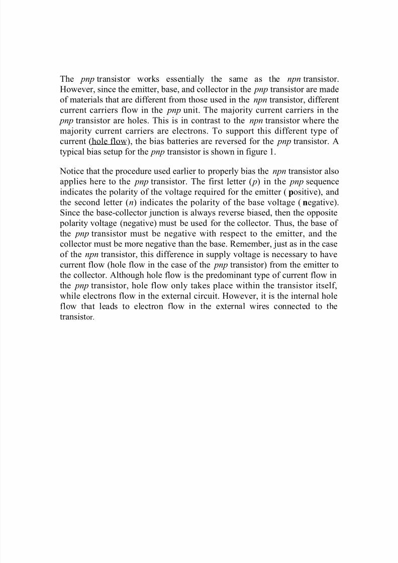
The pnp transistor works essentially the same as the npn transistor.
However, since the emitter, base, and collector in the pnp transistor are made
of materials that are different from those used in the npn transistor, differentcurrent carriers flow in the pnp unit. The majority current carriers in the
pnp transistor are holes. This is in contrast to the npn transistor where the
majority current carriers are electrons. To support this different type of
current (hole flow), the bias batteries are reversed for the pnp transistor. A
typical bias setup for the pnp transistor is shown in figure 1.
Notice that the procedure used earlier to properly bias the npn transistor also
applies here to the pnp transistor. The first letter ( p) in the pnp sequence
indicates the polarity of the voltage required for the emitter (positive), and
the second letter (n) indicates the polarity of the base voltage (negative).
Since the base-collector junction is always reverse biased, then the opposite
polarity voltage (negative) must be used for the collector. Thus, the base of
the pnp transistor must be negative with respect to the emitter, and the
collector must be more negative than the base. Remember, just as in the case
of the npn transistor, this difference in supply voltage is necessary to have
current flow (hole flow in the case of the pnp transistor) from the emitter to
the collector. Although hole flow is the predominant type of current flow in
the pnp transistor, hole flow only takes place within the transistor itself,
while electrons flow in the external circuit. However, it is the internal holeflow that leads to electron flow in the external wires connected to the
transistor.

7/30/2019 Shiri Automatic
http://slidepdf.com/reader/full/shiri-automatic 43/55
Figure 2: The forward-biased junction in a pnp transistor .
pnp Forward-Biased Junction
Now let us consider what happens when the emitter-base junction is forward
biased. With the bias setup shown, the positive terminal of the battery repels
the emitter holes toward the base, while the negative terminal drives the base
electrons toward the emitter. When an emitter hole and a base electron meet,they combine. For each electron that combines with a hole, another electron
leaves the negative terminal of the battery, and enters the base. At the same
time, an electron leaves the emitter, creating a new hole, and enters the
positive terminal of the battery. This movement of electrons into the base
and out of the emitter constitutes base current flow (IB), and the path these
electrons take is referred to as the emitter-base circuit.
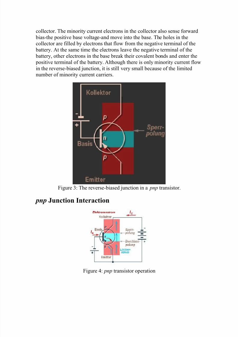
pnp Reverse-Biased Junction
In the reverse-biased junction (figure 3), the negative voltage on the
collector and the positive voltage on the base block the majority current
carriers from crossing the junction.
However, this same negative collector voltage acts as forward bias for the
minority current holes in the base, which cross the junction and enter the
7/30/2019 Shiri Automatic
http://slidepdf.com/reader/full/shiri-automatic 44/55
collector. The minority current electrons in the collector also sense forward
bias-the positive base voltage-and move into the base. The holes in the
collector are filled by electrons that flow from the negative terminal of the
battery. At the same time the electrons leave the negative terminal of the
battery, other electrons in the base break their covalent bonds and enter the
positive terminal of the battery. Although there is only minority current flow
in the reverse-biased junction, it is still very small because of the limited
number of minority current carriers.
Figure 3: The reverse-biased junction in a pnp transistor.
pnp Junction Interaction
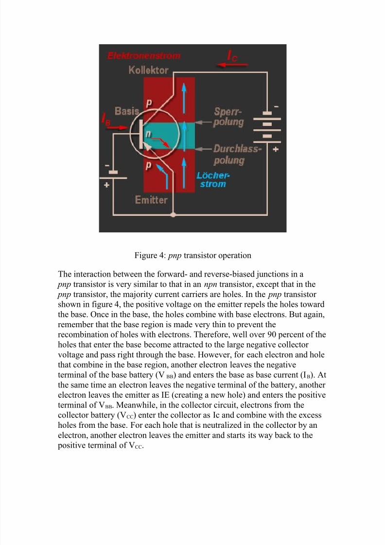
Figure 4: pnp transistor operation
7/30/2019 Shiri Automatic
http://slidepdf.com/reader/full/shiri-automatic 45/55
Figure 4: pnp transistor operation
The interaction between the forward- and reverse-biased junctions in a
pnp transistor is very similar to that in an npn transistor, except that in the pnp transistor, the majority current carriers are holes. In the pnp transistor
shown in figure 4, the positive voltage on the emitter repels the holes toward
the base. Once in the base, the holes combine with base electrons. But again,
remember that the base region is made very thin to prevent the
recombination of holes with electrons. Therefore, well over 90 percent of the
holes that enter the base become attracted to the large negative collector
voltage and pass right through the base. However, for each electron and hole
that combine in the base region, another electron leaves the negative
terminal of the base battery (V BB) and enters the base as base current (IB). At
the same time an electron leaves the negative terminal of the battery, another electron leaves the emitter as IE (creating a new hole) and enters the positive
terminal of VBB. Meanwhile, in the collector circuit, electrons from the
collector battery (VCC) enter the collector as Ic and combine with the excess
holes from the base. For each hole that is neutralized in the collector by an
electron, another electron leaves the emitter and starts its way back to the
positive terminal of VCC.

7/30/2019 Shiri Automatic
http://slidepdf.com/reader/full/shiri-automatic 46/55
Figure 3: total current flow in the pnp transistor
Figure 5: total current flow in the pnp transistor
Although current flow in the external circuit of the pnp transistor is opposite
in direction to that of the npn transistor, the majority carriers always flow
from the emitter to the collector. This flow of majority carriers also results in
the formation of two individual current loops within each transistor. One
loop is the base-current path, and the other loop is the collector-current path.
The combination of the current in both of these loops (IB + IC) results in total
transistor current (IE). The most important thing to remember about the two
different types of transistors is that the emitter-base voltage of the
pnp transistor has the same controlling effect on collector current as that of
the npn transistor. In simple terms, increasing the forward-bias voltage of a

7/30/2019 Shiri Automatic
http://slidepdf.com/reader/full/shiri-automatic 47/55
transistor reduces the emitter-base junction barrier. This action allows more
carriers to reach the collector, causing an increase in current flow from the
emitter to the collector and through the external circuit. Conversely, a
decrease in the forward-bias voltage reduces collector current.

7/30/2019 Shiri Automatic
http://slidepdf.com/reader/full/shiri-automatic 48/55
PCB MANUFACTURING
7/30/2019 Shiri Automatic
http://slidepdf.com/reader/full/shiri-automatic 49/55
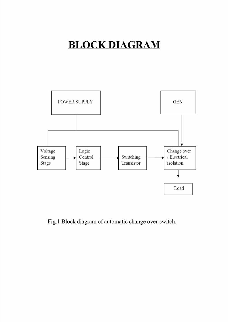
BLOCK DIAGRAM
Fig.1 Block diagram of automatic change over switch.

7/30/2019 Shiri Automatic
http://slidepdf.com/reader/full/shiri-automatic 50/55
CIRCUIT DIAGRAM
7/30/2019 Shiri Automatic
http://slidepdf.com/reader/full/shiri-automatic 51/55
WORKING
In three-phase applications, if lowvoltage is available in any one or two
phases, and you want your equipment to work on normal voltage, this circuit
will solve your problem. However, a proper-rating fuse needs to be used in
the input lines (R, Y and B) of each phase. The circuit provides correct
voltage in the same power supply lines through relays from the other phase
where correct voltage is available. Using it you can operate all
yourequipment even when correct voltage is available on a single phase inthe building.
The circuit is built around a transformer, comparator,transistor and relay. Three identical sets of this circuit, oneeach for three phases, are used. Let us now consider theworking of the circuit connecting red cable (call it ‘R’ phase).
The mains power supply phase R is stepped down bytransformer X1 to deliver 12V, 300 mA, which is rectified by
diode D1 and filtered by capacitor C1 to produce theoperating voltage for the operational amplifier(IC1). Thevoltage at inverting pin 2 of oprational amplifier IC1 is takenfrom the voltage divider circuit of resistor R1 and presetresistor VR1. VR1 is used to set the reference voltageaccording to the requirement. The reference voltage at non-inverting pin 3 is fixed to 5.1V through zener diode ZD1. Tillthe supply voltage available in phase R is in the range of 200V-230V, the voltage at inverting pin 2 of IC1 remains
high, i.e., more than reference voltage of 5.1V, and itsoutput pin 6 also remains high. As a result, transistor T1does not conduct, relay RL1 remains de-energised and phase‘R’ supplies power to load L1 via normallyclosed (N/C)contact of relay RL1.

7/30/2019 Shiri Automatic
http://slidepdf.com/reader/full/shiri-automatic 52/55
As soon as phase-R voltage goes below 200V, the voltage atinverting pin 2 of IC1 goes below reference voltage of 5.1V,and its output goes low. As a result, transistor T1 conductsand relay RL1 energises and load L1 is disconnected from
phase ‘R’ and connected to phase ‘Y’ through relay RL2.Similarly, the auto phase-change of the remaining twophases, viz, phase ‘Y’ and phase ‘B,’ can be explained.Switch S1 is mains power ‘on’/’off’ switch.
Use relay contacts of proper rating and fuses should be ableto take-on the load when transferred from other phases.While wiring, assembly and installation of the circuit, make
sure that you:1. Use good-quality, multi-strand insulated copper wiresuitable for your current requirement.2. Use good-quality relays with proper contact and currentrating.3. Mount the transformer(s) and relays on a suitable cabinet.Use a TagBlock (TB) for incoming/outgoing connections from mains.

7/30/2019 Shiri Automatic
http://slidepdf.com/reader/full/shiri-automatic 53/55
Planning of work
Choose project.
Collect information about project.
Arrange the components.
Testing the components.
Design the circuit.
Connect the components according to circuit.
Testing of circuit.
Checked by guide.
Final testing by project incharge.

7/30/2019 Shiri Automatic
http://slidepdf.com/reader/full/shiri-automatic 54/55
APPLICATION
Residential.
Commercial offices.
Factories operating with 1 phase machineries.
Hospitals/Banks.
Institutions.
It automatically supplies voltage in case of power failure or low voltagein up to 2 of the 3 incoming phases.
Automatic Phase Changer automatically cuts supply
during low voltage thus, protects equipment from the harmful affects of
unhealthily low voltage.

7/30/2019 Shiri Automatic
http://slidepdf.com/reader/full/shiri-automatic 55/55
BIBLOGRAPHY
Electronics for you(January 2009). Theraja, B.L.; and Theraja, A.K. 2002. Electrical Technology,
21st ed. Ranjendra Ravida, New Delhi, India.