PulseBlaster - Programmable Pulse
Generator
(PCIe Board SP35)
SP35 Model: PB24-100-4k
Owner’s Manual
SpinCore Technologies, Inc.http://www.spincore.com

PulseBlaster
Congratulations and thank you for choosing a design fromSpinCore Technologies, Inc.
We appreciate your business!
At SpinCore we aim to fully support the needs of our customers. Ifyou are in need of assistance, please contact us and we will strive to
provide the necessary support.
© 2000-2017 SpinCore Technologies, Inc. All rights reserved.SpinCore Technologies, Inc. reserves the right to make changes to the product(s) or information herein without notice. PulseBlaster™, SpinCore, and the SpinCore Technologies, Inc. logos are trademarks of SpinCore Technologies, Inc. All other trademarks are the property of their respective owners.
SpinCore Technologies, Inc. makes every effort to verify the correct operation of the equipment. This equipment version is not intended for use in a system in which the failure of a SpinCore device will threaten the safety of equipment or person(s).
http://www.spincore.com 2017/09/042

PulseBlaster
Table of ContentsI. Introduction .............................................................................................. 5
Product Overview ..................................................................................................... 5
Board Architecture ................................................................................................... 6Block Diagram ..................................................................................................... 6
Key Features .............................................................................................................. 6 Output Signals ..................................................................................................... 6Timing Characteristics .......................................................................................... 7Instruction Set ....................................................................................................... 7External Triggering ............................................................................................... 7Status Readback .................................................................................................. 7Summary .............................................................................................................. 7
Specifications ............................................................................................................ 8Pulse Parameters ................................................................................................. 8Pulse Program Control Flow ................................................................................ 8
Note on Related Boards Compatible with this Manual ......................................... 8
II. Installation ............................................................................................... 9
Installing the PulseBlaster ....................................................................................... 9
Testing the PulseBlaster ........................................................................................... 9
III. Programming the PulseBlaster .......................................................... 12
The PulseBlaster Interpreter .................................................................................. 12
PulseBlaster.NET ..................................................................................................... 13
LabVIEW Extensions ............................................................................................... 14
PulseBlaster Matlab GUI ......................................................................................... 15
C/C++ Programming ................................................................................................ 16
IV. Connecting to the PulseBlaster Board .............................................. 18
Connector Information ............................................................................................ 18Sketch of PulseBlaster PCIe .............................................................................. 18
Pin Assignments ..................................................................................................... 18DB25 Bracket Connector Flag 0..15 - Pin Assignments .................................... 18
http://www.spincore.com 2017/09/043

PulseBlasterSMA Connector Clock_Out ................................................................................ 19SMA Connector Ext_Clock ................................................................................. 19Shrouded IDC Connector Flag0..11 - Pin Assignments ..................................... 19Shrouded IDC Connector Flag12..23 - Pin Assignments ................................... 20Shrouded IDC Connector Flag24..26 - Pin Assignments ................................... 20Shrouded IDC Connector HW TRIG/RESET ..................................................... 21
Appendix I: Controlling the PulseBlaster with SpinAPI ........................ 23
Introduction .............................................................................................................. 23
Instruction Set Architecture ................................................................................... 23Machine-Word Definition .................................................................................... 23Breakdown of 80-bit Instruction Word ................................................................ 23
About SpinAPI ......................................................................................................... 26
Using C Functions to Program the PulseBlaster ................................................. 26Example Use of C Functions .............................................................................. 29
Appendix II: Sample C Program .............................................................. 30
Related Products and Accessories ......................................................... 32
Contact Information ................................................................................. 34
Document Information Page .................................................................... 34
http://www.spincore.com 2017/09/044

PulseBlaster
I. Introduction
Product Overview
The PulseBlaster device is an intelligent pulse/word/pattern generation unit producing 24
precisely timed, individually controlled digital output signals.
The intelligence of the PulseBlaster timing processor comes from an embedded
microprogrammed control core (uPC). The PulseBlaster processor is able to execute instructions that
allow it to control program flow. This means that the PulseBlaster processor understands Operational
Control Codes, OpCodes, and will execute them much the same way as a general-purpose
microprocessor does. The PulseBlaster’s microcontroller is different from the general-purpose
microprocessor in that it does not contain an arithmetic logic unit (ALU) and is, therefore, incapable of
doing mathematical or logical calculations. However, a unique and distinguishing feature of the
PulseBlaster processor is that the execution time of instructions is user programmable. This feature
makes the PulseBlaster capable of executing complex output timing patterns at greatly varying
update rates, ranging from nanoseconds to years, with a constant setting accuracy of just one clock
period (e.g., a 10 ns setting accuracy at a 100 MHz clock frequency).
http://www.spincore.com 2017/09/045

PulseBlasterBoard Architecture
Block Diagram
Figure 1 presents the general architecture of the PulseBlaster system. The major building blocks
are the SRAM memory (both internal and external to the processor), the microcontroller (uPC), the
integrated bus controller (IBC), the counter, and the output buffers. The entire logic design, excluding
output buffers, is contained on a single silicon chip, making it a System-on-a-Chip design. User
control to the system is provided through the IBC over the peripheral component interconnect (PCIe)
bus.
Figure 1: PulseBlaster board architecture. The clock oscillator signal is derived from an on-chip PLL circuit
typically using a 50 MHz on-board reference clock.
Key Features
Output Signals
The PulseBlaster PB24 PCIe board allows for 24 digital output signal lines. Sixteen output lines
are routed to a DB25 bracket-mounted connector. All 24 output lines are available for routing to IDCs.
The 24 individually controlled digital output lines comply with the transistor-transistor logic (TTL)
levels’ standard, and are capable of delivering up to 20 mA per bit/channel. If more output current is
necessary, the individual bits/channels can be driven in parallel.
http://www.spincore.com 2017/09/046
PCI BusPCI Bus

PulseBlasterTiming Characteristics
The PulseBlaster’s timing controller accepts an internal (on-board) crystal oscillator up to 100
MHz. The innovative architecture of the timing controller allows the processing of either simple timed
instructions (with delays of up to 232 or 4,294,967,296 clock cycles), or double-length timed
instructions (up to 252 clock cycles long – nearly 2 years with a 100 MHz clock!). Regardless of the
type of instruction, the timing resolution remains constant for any delay – just one clock period (e.g.,
10 ns at 100 MHz).
The core-timing controller has a minimum delay cycle of five clock periods for the PB24-100-4k
model. For a 100 MHz clock, this translates to a 50.0 ns pulse/delay/update.
Instruction Set
The PulseBlaster’s design features a set of commands for highly flexible program flow control.
The micro-programmed controller allows for programs to include branches, subroutines, and loops at
up to 8 nested levels – all this to assist the user in creating dense pulse programs that cycle through
repetitious events, especially useful in numerous multidimensional spectroscopy and imaging
applications.
External Triggering
The PulseBlaster can be triggered and/or reset externally via dedicated hardware lines. These
lines combine the convenience of triggering (e.g., in cardiac gating) with the safety of the "stop/reset"
line. The required control signals are active-low (or short to ground), with additional active-high pins
available.
Status Readback
The status of the pulse program can be read through software using C. See Appendix I
(Controlling the PulseBlaster with SpinAPI, page 23) for more detail about the C function
pb_read_status().
Summary
The PulseBlaster is a versatile, high-performance, programmable pulse/pattern TTL signal
generator operating at speeds of 100 MHz and capable of generating pulses/delays/intervals ranging
from 50 ns to two years per instruction. It is connected via PCIe port and can accommodate pulse
programs with highly flexible control commands of up to 4k (i.e., 4096) program words (Model PB24-
100-4k). Its high-current output logic bits are independently controlled with a voltage of 3.3 V.
http://www.spincore.com 2017/09/047

PulseBlasterSpecifications
Pulse Parameters
24 individually controlled digital output lines (TTL levels, 3.3 V logical “one”) Variable pulses/delays for every TTL line Up to 20 mA output current per TTL line 50 ns shortest pulse/interval for internal memory model PB24-100-4k 2 years longest pulse interval (at 100 MHz, with the use of the “Long Delay” instruction) 10 ns pulse/interval resolution (at 100 MHz) Up to 4k pulse program memory words/instructions for model PB24-100-4k External triggering and reset – TTL levels
Pulse Program Control Flow
Loops, nested 8 levels deep 20 bit loop counters (max. 1,048,576 repetitions) Subroutines, nested 8 levels deep Latency after trigger (WAIT state) – 8 clock cycle latency (80 ns at 100 MHz), adjustable to 40
seconds in duration 5 MHz max. re-triggering frequency (at 100 MHz clock frequency)
Note on Related Boards Compatible with this Manual
Much of the programming information provided in this manual is nearly universal to SpinCore's
lines of boards. More complex boards such as the PulseBlasterESR, PulseBlaster-DDS, and
RadioProcessor lines of boards still rely on the same PulseBlaster core for TTL pulse generation.
Therefore, the basic example programs for the PulseBlaster will be able to produce the same results
on any of the more complex boards. The exception is the PulseBlaster-DDS-II board which uses a
96-Bit or 124-Bit instruction word, depending on the firmware, instead of an 80-Bit instruction word
and is currently not compatible with PulseBlaster methods of programming the board.
http://www.spincore.com 2017/09/048

PulseBlaster
II. Installation
Installing the PulseBlaster
Whenever installing or uninstalling the PulseBlaster, always have it disconnected from the
computer. Uninstall any previous version of SpinAPI.
1. Install the preliminary version of SpinAPI for the SP35 board found at:
http://spincore.com/CD/Setup/SP35/ .
• SpinAPI is a custom Application Programming Interface developed by SpinCore
Technologies, Inc. for use with the PulseBlaster and most of SpinCore's other products. It
can be utilized using C/C++ or graphically using the options in the next section below. The
API will also install the necessary drivers.
2. Shut down the computer, unplug the power cord, insert the PulseBlaster card into an available
PCIe slot and fasten the PC bracket securely with a screw.
3. Plug the power cord back in, turn on the computer and follow the installation prompts.
Testing the PulseBlaster
The simplest way to test whether the has been installed properly and can be controlled as
intended is to run a simple test program. These example files can be found in the SpinAPI package.
To open the SpinAPI package on a Windows 10 PC, simply click the Window Start icon, and
scroll down to find and open the "spincore" folder. Example .exe files and their C source code can be
found in the folder /SpinAPI/examples. From there, you may select the “PulseBlaster24” folder and
run all .exe programs to test your PulseBlaster.
The pb24_ex1.exe program will produce a square wave, on all digital outputs, with a logical
high time of 200 ms and logical low time of 200 ms. To test the board, run pb24_ex1.exe and observe
each digital output with an oscilloscope.
http://www.spincore.com 2017/09/049
PulseBlaster
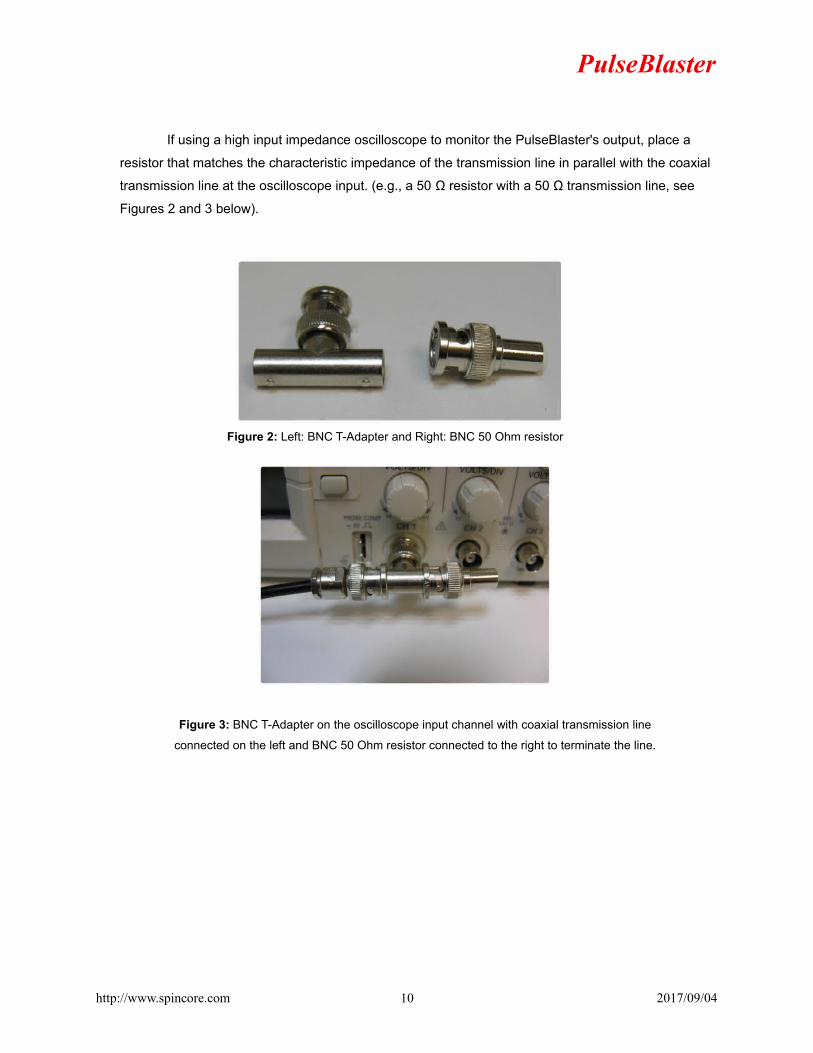
If using a high input impedance oscilloscope to monitor the PulseBlaster's output, place a
resistor that matches the characteristic impedance of the transmission line in parallel with the coaxial
transmission line at the oscilloscope input. (e.g., a 50 Ω resistor with a 50 Ω transmission line, see
Figures 2 and 3 below).
http://www.spincore.com 2017/09/0410
Figure 2: Left: BNC T-Adapter and Right: BNC 50 Ohm resistor
Figure 3: BNC T-Adapter on the oscilloscope input channel with coaxial transmission line
connected on the left and BNC 50 Ohm resistor connected to the right to terminate the line.

PulseBlaster
Figure 4 below shows a typical pattern displayed by an oscilloscope when running pb24_ex1.exe
with the above described connections. Verifying this behavior confirms the board is installed properly.
You may also run the remaining example programs available for this board to observe different
output patterns and pulse durations. Keep in mind that pb24_programmable_clock.exe is only
compatible with PulseBlasters with the programmable clock feature which is available upon request.
http://www.spincore.com 2017/09/0411
Figure 4: Expected signal from a PulseBlaster output running pb24_ex1.exe. Note that the
high state is 2.52V instead of 3.3V because the 50 Ohm resistor load and current
limitations for the pin.
PulseBlaster
III. Programming the PulseBlaster
There are several ways of programming the PulseBlaster board. In this section the PulseBlaster
Interpreter, LabVIEW extensions, .NET GUI, MATLAB GUI, and C/C++ methods of programming will
be introduced. In addition to these, the PulseBlaster is programmable using nearly any higher level
programming software that lets you utilize a C language API package, in this case SpinCore's
SpinAPI.
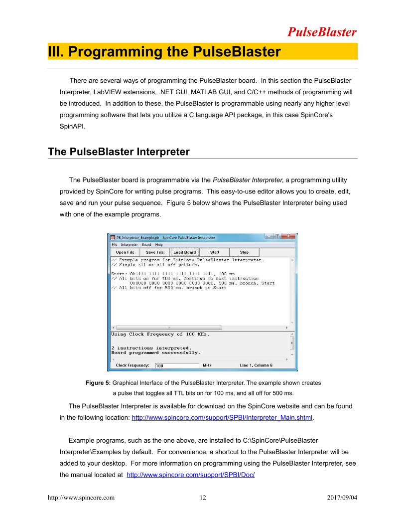
The PulseBlaster Interpreter
The PulseBlaster board is programmable via the PulseBlaster Interpreter, a programming utility
provided by SpinCore for writing pulse programs. This easy-to-use editor allows you to create, edit,
save and run your pulse sequence. Figure 5 below shows the PulseBlaster Interpreter being used
with one of the example programs.
The PulseBlaster Interpreter is available for download on the SpinCore website and can be found
in the following location: http://www.spincore.com/support/SPBI/Interpreter_Main.shtml.
Example programs, such as the one above, are installed to C:\SpinCore\PulseBlaster
Interpreter\Examples by default. For convenience, a shortcut to the PulseBlaster Interpreter will be
added to your desktop. For more information on programming using the PulseBlaster Interpreter, see
the manual located at http://www.spincore.com/support/SPBI/Doc/
http://www.spincore.com 2017/09/0412
Figure 5: Graphical Interface of the PulseBlaster Interpreter. The example shown creates
a pulse that toggles all TTL bits on for 100 ms, and all off for 500 ms.

PulseBlasterPulseBlaster.NET
PulseBlaster.NET is a graphical interface for creating pulse programs and loading them to the
PulseBlaster board. PulseBlaster.NET currently provides the simplest interface possible to pulse
control. Figure 3 shows an example instance of the program.
PulseBlaster.NET is available on the web from http://www.spincore.com/support/net/.
http://www.spincore.com 2017/09/0413
Figure 6: An example pulse program in PulseBlaster.NET. This example creates a pulse that has all TTL bits on for
100 ms, alternating bits on for 400 ms (looping three times), and then all bits off for 100 ms.

PulseBlasterLabVIEW Extensions
The SpinCore PulseBlaster LabVIEW Extensions (PBLV) provide the ability to program and control
the functionality of PulseBlaster boards using the simple National Instruments (NI) LabVIEW
graphical programming interface. The package contains basic subVIs that can be used to include
PulseBlaster interaction from your own LabVIEW programs, as well as some complete example VIs.
Additionally, all of the examples are available as stand-alone applications, so that no programming is
necessary for use.
There are two versions of the LabVIEW extensions available free of charge on SpinCore's
website. The first is for those who do not have LabVIEW or who are not familiar with LabVIEW
programming. This option is a stand-alone GUI (see Figure 7 above) that comes in executable form
and utilizes the LabVIEW runtime environment. The second is for those who have LabVIEW and
http://www.spincore.com 2017/09/0414
Figure 7: Example of PulseBlaster LabVIEW Extensions User
Interface. The example shown has three instructions that toggle
TTL bit 1 on for 200 ms and off for 200 ms.

PulseBlasterwould like to make a custom interface for the PulseBlaster board. For more information and
downloads please visit:
http://www.spincore.com/support/PBLV/TTL.shtml
PulseBlaster Matlab GUI
PulseBlaster Matlab GUI is a graphical interface for creating pulse programs and loading them to
the PulseBlaster board. PulseBlaster Matlab GUI currently provides the simplest interface possible to
pulse control. Figure 8 shows an example instance of the program.
PulseBlaster Matlab GUI is available at: http://www.spincore.com/support/PulseBlasterMatlabGUI/.
http://www.spincore.com 2017/09/0415
Figure 8: An example pulse program in PulseBlaster Matlab GUI.

PulseBlasterC/C++ Programming
The most dynamic and flexible way to program the PulseBlaster board is with C/C++ using the
SpinAPI package. The GUI based approaches to programming the board are designed for simplicity
so they can be used by someone with no programming experience. While GUI's are easier to use,
coding in C/C++ allows you to better utilize all features of the board, and in some cases it may be
easier to copy and paste lines of code than to make 100 instructions on a GUI. With the pre-
configured compiler package available on our website, changing one of our example programs and
recompiling the executable file for use with your PulseBlaster board is as easy as clicking “Rebuild
All” (see Figure 9 below). The free pre-configured compiler package is available at the following URL,
under the “Windows Pre-configured Compiler” heading:
http://www.spincore.com/support/spinapi/
Making changes to an example program requires understanding of only a few lines of code. The
most important is the following line from pb24_ex1.c (found in C:\SpinCore\Examples\PulseBlaster24
if the examples were installed in the default directory):
pb_inst(0xFFFFFF, CONTINUE, 0, 200.0*ms);
http://www.spincore.com 2017/09/0416
Figure 9: Compiling a C program to run the PulseBlaster board is easy!

PulseBlasterThis line of code produces a high output on all the TTL bits lasting for 200 ms and then continues
on to the next instruction. This is accomplished using the four parameters in the function call
(parameters are located between parentheses and are separated by commas).
• The first is the hexadecimal 0xFFFFFF which corresponds to setting the 24 output bits to a
logical high since it translates to a binary string of 24 1's.
• The second parameter is CONTINUE which means to proceed on to the next instruction after
this one completes. Other examples for what this parameter could be are BRANCH or LOOP.
• The third parameter is the instruction data field which, for a CONTINUE instruction, is ignored
because it is unnecessary for that particular instruction. In the event of another instruction,
such as BRANCH, this parameter would correspond to the target of the BRANCH instruction.
• The fourth parameter is 200.0*ms which means that this instruction will last for 200 ms.
A simple program to generate a square wave signal on all 24 output bits will have two intervals (as
in the GUI Interpreter described earlier), as shown below:
start= pb_inst(0xFFFFFF, CONTINUE, 0, 200.0*ms);
pb_inst(0x000000, BRANCH, start, 200.0*ms);
The first line of the code above corresponds to the logical "one” on all output bits. The second line
corresponds to the logical "zero," after which the program branches (jumps) back to the beginning,
thus resulting in a continuous generation of a square wave on all outputs.
A complete C program will have, in addition to the two lines above, the initialization section, the
closing section and, optionally, the (software) trigger to start the execution immediately upon launch
of the program. For more detailed information on programming the board using C/C++ see the
appendices.
http://www.spincore.com 2017/09/0417

PulseBlaster
IV. Connecting to the PulseBlaster Board
Connector Information
Sketch of PulseBlaster PCIe
Pin Assignments
DB25 Bracket Connector Flag 0..15 - Pin Assignments
Outputs 16 TTL signals generated by the user’s program. Please consult the table below for bit
assignments.
Pin AssignmentsPin# Bit# Pin# Bit#
1 GND 14 GND2 Bit 15 15 Bit 143 GND 16 Bit 134 Bit 12 17 GND5 Bit 11 18 Bit 106 GND 19 Bit 97 Bit 8 20 GND8 Bit 7 21 Bit 69 GND 22 Bit 5
10 Bit 4 23 GND11 Bit 3 24 Bit 212 GND 25 Bit 113 Bit 0
Table 1: Lower 16 output bits and 9 ground lines on the bracket-mounted DB25 connector.
http://www.spincore.com 2017/09/0418
Figure 10: On the board the Clock_Out and Ext_Clk are SMA connectors, Flag0..15 is a DB-25 connector, Flag0..11,
Flag12..23, Flag24..26, and HW TRIG/RESET are shrouded IDC header connectors.

PulseBlaster
SMA Connector Clock_Out
This SMA connector outputs the reference clock as a 3.3 V TTL signal, i.e., it generates positive-
only voltage. Note that the boards use 50 MHz as the reference clock frequency and that clock is
internally multiplied to provide that actual PulseBlaster Core frequency. The output resembles a
square wave if properly terminated. This signal can be measured with an oscilloscope using either a
high impedance probe at the SMA connector or a 50 ohm coaxial line that is terminated.
SMA Connector Ext_Clock
This SMA connector can be used to input an external clock signal. Extreme care should be
exercised, and certain conditions have to be met prior to using this connector. First, before attaching
any external clock source, the internal clock oscillator must be removed from its socket. The internal
clock oscillator’s orientation should be noted - if the internal clock is reconnected, it must be inserted in
the same orientation or board damage may occur. Second, the external clock signal must be 3.3 V
TTL, i.e., a positive-only voltage - any negative voltage at the Ext_Clk connector will damage the
programmable-logic processor chip. Third, as the Ext-Clk connector is not terminated on the printed
circuit board, a 50 ohm terminating resistor should be used externally via a T connector placed directly
at the SMA Ext_Clk connector. Alternatively, a 50 ohm resistor could be soldered on the board on
R001 pads.
Shrouded IDC Connector Flag0..11 - Pin Assignments
The shrouded IDC connector labeled Flag 0..11 outputs TTL signals generated by the user’s
program. Please consult the table below for pin assignments.
Pin AssignmentsPin# Pin#
1 Bit 0 13 Bit 62 GND 14 GND3 Bit 1 15 Bit 74 GND 16 GND5 Bit 2 17 Bit 86 GND 18 GND7 Bit 3 19 Bit 98 GND 20 GND9 Bit 4 21 Bit 10
10 GND 22 GND11 Bit 5 23 Bit 1112 GND 24 GND
Table 2: Lower 12 output bits and 12 ground lines on the 24 pin IDC connector.
http://www.spincore.com 2017/09/0419
PulseBlaster
The shrouded IDC connector labeled Flag 0..11 can also be accessed using an SP32 board
(Figure 13) which allows the use of MMCX cables. This enables the individual bits of the PulseBlaster to
be more easily accessed. Pin 1 on the MMCX adapter board can identified with a square pin.
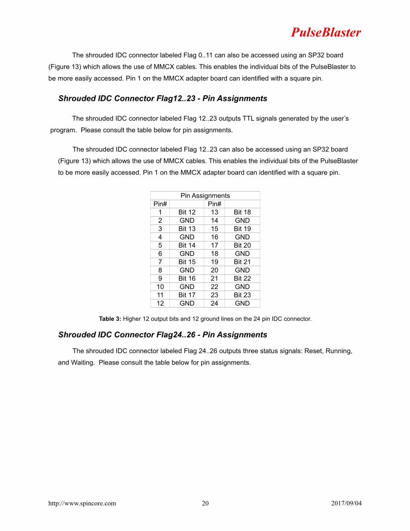
Shrouded IDC Connector Flag12..23 - Pin Assignments
The shrouded IDC connector labeled Flag 12..23 outputs TTL signals generated by the user’s
program. Please consult the table below for pin assignments.
The shrouded IDC connector labeled Flag 12..23 can also be accessed using an SP32 board
(Figure 13) which allows the use of MMCX cables. This enables the individual bits of the PulseBlaster
to be more easily accessed. Pin 1 on the MMCX adapter board can identified with a square pin.
Pin AssignmentsPin# Pin#
1 Bit 12 13 Bit 182 GND 14 GND3 Bit 13 15 Bit 194 GND 16 GND5 Bit 14 17 Bit 206 GND 18 GND7 Bit 15 19 Bit 218 GND 20 GND9 Bit 16 21 Bit 22
10 GND 22 GND11 Bit 17 23 Bit 2312 GND 24 GND
Table 3: Higher 12 output bits and 12 ground lines on the 24 pin IDC connector.
Shrouded IDC Connector Flag24..26 - Pin Assignments
The shrouded IDC connector labeled Flag 24..26 outputs three status signals: Reset, Running,
and Waiting. Please consult the table below for pin assignments.
http://www.spincore.com 2017/09/0420

PulseBlasterPin Assignments
Pin# Pin#1 Reset 13 GND2 GND 14 GND3 Running 15 GND4 GND 16 GND5 Waiting 17 GND6 GND 18 GND7 GND 19 GND8 GND 20 GND9 GND 21 GND
10 GND 22 GND11 GND 23 GND12 GND 24 GND
Table 4: 3 status signals and 21 ground lines on the 24 pin IDC connector.
The status pins correspond to the current state of the pulse program and are defined as follows:
Reset – Driven high when the PulseBlaster device is in a RESET state and must be
reprogrammed before code execution can begin again.
Running – Driven high when the PulseBlaster device is executing a program. It is low when the
PulseBlaster enters either a reset or idle state.
Waiting – the PulseBlaster device has encountered a WAIT Op Code and is waiting for the next
trigger (either hardware or software) to resume operation. Note that the Running bit will also be
high during a WAIT state.
Shrouded IDC Connector HW TRIG/RESET
This is an input connector, for hardware triggering (HW_Trigger) and resetting (HW_Reset).
Pin AssignmentsPin# Pin#
1 GND 2 HW_Trigger_H3 GND 4 HW_Trigger_H5 GND 6 HW_Reset_H7 GND 8 HW_Reset9 GND 10 HW_Trigger
Table 5: Pinout for HW TRIG/RESET IDC connector.
In addition to the standard active-low HW_Trigger pin, this board has two active-high
HW_Trigger_H pins. The functionality of these three pins are identical, however, the HW_Trigger pin
is pulled high on board and therefore can be triggered by a low pulse (or shorting to GND, i.e., pin 9).
The HW_Trigger_H pins are pulled low on board and can be triggered by a high pulse. This trigger
http://www.spincore.com 2017/09/0421

PulseBlasterwill restart execution of a program from the beginning of the code if it is detected after the design has
reached an idle state. The idle state could have been created either by reaching the STOP Op Code
of a program, or by the detection of the HW_Reset signal. If the STOP Op Code is used, a
HW_Reset or software reset (pb_reset()) needs to be applied prior to the HW_Trigger. When the
WAIT Op Code is used in the pulse program, the HW_Trigger will cause the program to continue to
the next instruction.
In addition to the standard active-low HW_Reset pin, this board has one active-high
HW_Reset_H pin. The functionality of these two pins are identical, however, the HW_Reset pin is
pulled high on board and therefore can be activated by a low pulse (or shorting to GND, i.e., pin 7).
The HW_Reset_H pin is pulled low on board and can be activated by a high pulse. When the signal
is activated during the execution of a program, the controller resets itself back to the beginning of the
program. Program execution can be resumed by either a software start command or by a hardware
trigger.
Note that for all board models the IDC pins are enumerated in the manner shown by Figure 11.
Pin 1 is marked on the board and the rest of the pins follow in this fashion (for the 26 pin IDC
connectors, the pin numbers simply continue in this pattern until pin 26).
http://www.spincore.com 2017/09/0422
Figure 11: IDC connector pin enumeration.
PulseBlasterAppendix I: Controlling the PulseBlaster with SpinAPI
Introduction
This section provides detailed descriptions of the instruction set for the processor on the
PulseBlaster board and the C functions in SpinAPI that utilize them. The information on the
instruction set is very in depth and knowledge of this is essential to be able to properly operate the
board. Details of the instruction set architecture are provided first so that the user can understand the
functionality of the PulseBlaster. The second part provides information about SpinCore's Application
Programming Interface (API) package, called SpinAPI.
Instruction Set Architecture
Machine-Word Definition
The PulseBlaster pulse timing and control processor implements an 80-bit wide Very Long
Instruction Word (VLIW) architecture. The VLIW memory words have specific bits/fields dedicated to
specific purposes, and every word should be viewed as a single instruction of the micro-controller.
The maximum number of instructions that can be loaded to on-chip memory is equal to the memory
size described in the model number (i.e., 4k memory words for Model PB24-100-4k). The execution
time of instructions can be varied and is under (self) control by one of the fields of the instruction word
– the shortest being five clock cycles for the “Internal Memory Model” and nine clock cycles for the
“External Memory Model.” All instructions have the same format and bit length, and all bit fields have
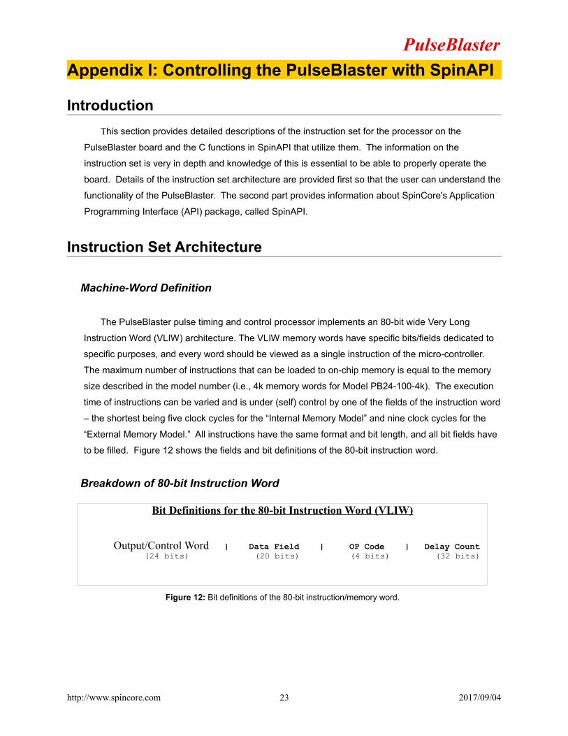
to be filled. Figure 12 shows the fields and bit definitions of the 80-bit instruction word.
Breakdown of 80-bit Instruction Word
http://www.spincore.com 2017/09/0423
Figure 12: Bit definitions of the 80-bit instruction/memory word.
Bit Definitions for the 80-bit Instruction Word (VLIW)
Output/Control Word | Data Field | OP Code | Delay Count (24 bits) (20 bits) (4 bits) (32 bits)
PulseBlasterThe 80-bit VLIW is broken up into 4 sections:
1. Output Pattern and Control Word - 24 bits
2. Data Field - 20 bits
3. OP Code - 4 bits
4. Delay Count - 32 bits
Output Pattern and Control Word
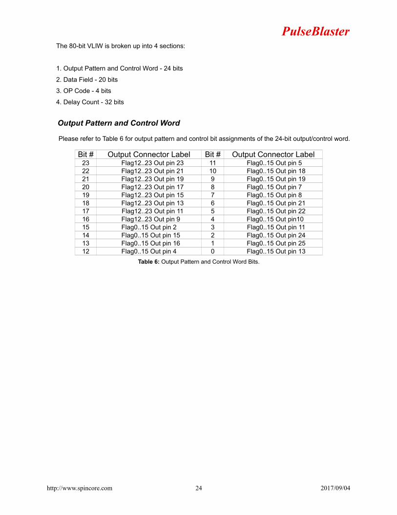
Please refer to Table 6 for output pattern and control bit assignments of the 24-bit output/control word.
Bit # Output Connector Label Bit # Output Connector Label23 Flag12..23 Out pin 23 11 Flag0..15 Out pin 522 Flag12..23 Out pin 21 10 Flag0..15 Out pin 1821 Flag12..23 Out pin 19 9 Flag0..15 Out pin 1920 Flag12..23 Out pin 17 8 Flag0..15 Out pin 719 Flag12..23 Out pin 15 7 Flag0..15 Out pin 818 Flag12..23 Out pin 13 6 Flag0..15 Out pin 2117 Flag12..23 Out pin 11 5 Flag0..15 Out pin 2216 Flag12..23 Out pin 9 4 Flag0..15 Out pin1015 Flag0..15 Out pin 2 3 Flag0..15 Out pin 1114 Flag0..15 Out pin 15 2 Flag0..15 Out pin 2413 Flag0..15 Out pin 16 1 Flag0..15 Out pin 2512 Flag0..15 Out pin 4 0 Flag0..15 Out pin 13
Table 6: Output Pattern and Control Word Bits.
http://www.spincore.com 2017/09/0424

PulseBlasterData Field and Op Code
Please refer to Table 7 for information on the available operational codes (OpCode) and the
associated data field functions (the data field's function is dependent on the OpCode).
Op Code # Inst Inst_data Function
0 CONTINUE IgnoredProgram execution continues to next
instruction.
1 STOP IgnoredStop execution of program. Aborts the
operation of the micro-controller. (Pleasesee note below)
2 LOOPNumber of desired loops. Thisvalue must be greater than or
equal to 1.
Specify beginning of a loop. Executioncontinues to next instruction. Data used to
specify number of loops.
3 END_LOOP Address of beginning of loopSpecify end of a loop. Execution returns to
beginning of loop and decrements loopcounter.
4 JSRAddress of first subroutine
instructionProgram execution jumps to beginning of a
subroutine.
5 RTS IgnoredProgram execution returns to instruction
after JSR was called.
6 BRANCH Address of next instructionProgram execution continues at specified
instruction.
7 LONG_DELAYDelay multiplier. This value
must be greater than or equal to2.
For long interval instructions. Executeslength of pulse given in the time field
multiplied by the value in the data field.
8 WAIT Ignored
Program execution stops and waits forsoftware or hardware trigger. Execution
continues to next instruction after receipt oftrigger. A WAIT instruction must be preceded
by an instruction lasting longer than theminimum instruction time.
Table 7: Op Code and Data Field Description.
Delay Count
The value of the Delay Count field (a 32-bit value) determines how long the current instruction
should be executed. The allowed minimum value of this field is 0x00000002 for the 4k and
0x00000006 for the 32k models, and the allowed maximum is 0xFFFFFFFF. The timing controller has
a fixed delay of three clock cycles and the value that one enters into the Delay Count field should
account for this inherent delay. (NOTE: the pb_inst() family of functions in SpinAPI and the
PulseBlaster Interpreter automatically account for this delay.)
http://www.spincore.com 2017/09/0425

PulseBlasterAbout SpinAPI
SpinAPI is a control library which allows programs to be written to communicate with the
PulseBlaster board. The most straightforward way to interface with this library is with a C/C++
program, and the API definitions are described in this context. However, virtually all programming
languages and software environments (including software such as LabView and Matlab) provide
mechanisms for accessing the functionality of standard libraries such as SpinAPI.
Please see the example programs for an an explanation of how to use SpinAPI. A reference
document for all SpinAPI functions is available online at the following URL under the “Windows
Drivers and Example Programs” heading, at the “API Reference” link:
http://www.spincore.com/support/spinapi/
For a pre-configured compiler for writing and modifying pulse programs download Dev-C++ with
MinGW from our website at the URL above under the “Windows Pre-configured Compiler” heading.
Using C Functions to Program the PulseBlaster
A series of functions have been written to control the board and facilitate the construction of pulse
program instructions.
In order to use these functions, the DLL (spinapi.dll), the library file (libspinapi.a for mingw,
spinapilibgcc for Borland, and spinapi.lib for MSVC), the header file (spinapi.h), must be in the
working directory of your C compiler1.
int pb_init();
Initializes PulseBlaster board. Needs to be called before calling any functions using the
PulseBlaster. Returns a negative number on an error or 0 on success.
int pb_close();
Releases PulseBlaster board. Needs to be called as last command in pulse program. Returns a
negative number on an error or 0 on success.
1 These functions and library files have been generated and tested with MinGW (www.mingw.com), Borland 5.5 (www.borland.com), MS Visual Studio 2003 (msdn.microsoft.com) compilers.
http://www.spincore.com 2017/09/0426

PulseBlasterint pb_core_clock(double clock_freq);
Used to set the clock frequency of the board. The variable clock_frequency is specified in MHz
when no units are entered. Valid units are MHz, kHz, and Hz. The default clock value is 50MHz.
You only need to call this function if you are not using a –50 board. Please contact SpinCore for
more information if needed.
int start_programming(int device);
Used to initialize the system to receive programming information. It accepts a parameter
referencing the target for the instructions. The only valid value for device is PULSE_PROGRAM, It
returns a 0 on success or a negative number on an error.
int pb_inst(int flags, int inst, int inst_data, double length);
Used to send one instruction of the pulse program. Should only be called after
start_programming(PULSE_PROGRAM) has been called. It returns a negative number on an
error, or the instruction number upon success. If the function returns –99, an invalid parameter
was passed to the function. Instructions are numbered starting at 0.
int flags – determines state of each TTL output bit. Valid values are 0x0 to 0xFFFFFF. For
example, 0x010 would correspond to bit 4 being on, and all other bits being off.
int inst – determines which type of instruction is to be executed. Please see Table 7 for details.
int inst_data – data to be used with the previous inst field. Please see Table 7 for details.
double length – duration of this pulse program instruction, specified in nanoseconds (ns).
int stop_programming();
Used to tell that programming the board is complete. Board execution cannot start until this
command is received. It returns a 0 on success or a negative number on an error.
int pb_start();
Once board has been programmed, this instruction will start execution of pulse program. It
returns a 0 on success or a negative number on an error.
http://www.spincore.com 2017/09/0427

PulseBlasterint pb_stop();
Stops output of board. Analog output will return to ground, and TTL outputs will remain in the
state they were in when stop command was received. It returns a 0 on success or a negative
number on an error.
int pb_read_status();
Read status from the board. Each bit of the returned integer indicates whether the board is in that
state. Bit 0 is the least significant bit.
● Bit 0 – Stopped
● Bit 1 - Reset
● Bit 2 – Running
● Bit 3 – Waiting
● Bit 4 - Scanning (RadioProcessor boards only)
Note on Bit 1: Bit 1 will be high, '1', as soon as the board is initialized. It will remain high until a
hardware or software reset occurs. At that point, it will stay low, '0', until the board is triggered
again.
Bits 5-31 are reserved for future use. It should not be assumed that these will be set to 0.
char* pb_get_version();
Returns the version of SpinAPI in the form YYYYMMDD, i.e. 20090209. This function should be
used to make sure you are using an up to date version of SpinAPI.
int pb_select_board(int board_num);
If multiple boards from SpinCore Technologies are present in your system, this function allows
you to select which board to communicate with. Once this function is called, all subsequent
commands (such as pb_init(), pb_core_clock(), etc.) will be sent to the selected board. You may
change which board is selected at any time. If you have only one board, it is not necessary to call
this function. All PCI slot boards are numbered before any USB boards, starting with the number
0. This function returns a 0 upon success, and a negative number upon failure.
http://www.spincore.com 2017/09/0428

PulseBlaster
Example Use of C Functions/* * PulseBlaster example 1 * This program will cause the outputs to turn on and off with a period * of 400ms */#include <stdio.h>#define PB24#include "spinapi.h"
int main(){
int start, status;
printf ("Using spinapi library version %s\n", pb_get_version());
if(pb_init() != 0) { printf ("Error initializing board: %s\n", pb_get_error());
return -1; }
// Tell the driver what clock frequency the board has (in MHz) pb_core_clock(100.0);
pb_start_programming(PULSE_PROGRAM);
// Instruction 0 - Continue to instruction 1 in 200ms// Flags = 0xFFFFFF, OPCODE = CONTINUEstart = pb_inst(0xFFFFFF, CONTINUE, 0, 200.0*ms);
// Instruction 1 - Continue to instruction 2 in 100ms // Flags = 0x0, OPCODE = CONTINUE pb_inst(0x0, CONTINUE, 0, 100.0*ms);
// Instruction 2 - Branch to "start" (Instruction 0) in 100ms // 0x0, OPCODE = BRANCH, Target = start pb_inst(0x0, BRANCH, start, 100.0*ms);
pb_stop_programming();
// Trigger the pulse programpb_start();
//Read the status registerstatus = pb_read_status();printf("status: %d", status);
pb_close();
return 0;}
A more complex program using C Functions is provided in Appendix II.
http://www.spincore.com 2017/09/0429

PulseBlaster
Appendix II: Sample C Program //* * PulseBlaster example 2 * This example makes use of all instructions (except WAIT). */#include <stdio.h>#define PB24#include <spinapi.h>
int main(int argc, char **argv){int start, loop, sub;int status;
printf ("Using spinapi library version %s\n", pb_get_version()); if(pb_init() != 0) { printf ("Error initializing board: %s\n", pb_get_error()); return -1; }
// Tell the driver what clock frequency the board has (in MHz) pb_core_clock(100.0);
pb_start_programming(PULSE_PROGRAM);
// Since we are going to jump forward in our program, we need to // define this variable by hand. Instructions start at 0 and count up
sub = 5;
// Instruction format // int pb_inst(int flags, int inst, int inst_data, int length)
// Instruction 0 - Jump to Subroutine at Instruction 5 in 1s start = pb_inst(0xFFFFFF,JSR, sub, 1000.0 * ms);
// Loop. Instructions 1 and 2 will be repeated 3 times // Instruction 1 - Beginning of Loop (Loop 3 times). Continue to next
// instruction in 1s loop = pb_inst(0x0,LOOP,3,150.0 * ms);
// Instruction 2 - End of Loop. Return to beginning of loop or // continue to next instruction in .5 s
pb_inst(0xFFFFFF,END_LOOP,loop,150.0 * ms);
// Instruction 3 - Stay here for (5*100ms) then continue to Instruction// 4
pb_inst(0x0,LONG_DELAY,5, 100.0 * ms);
// Instruction 4 - Branch to "start" (Instruction 0) in 1 s pb_inst(0x0,BRANCH,start,1000.0*ms);
// Subroutine // Instruction 5 - Continue to next instruction in 1 * s pb_inst(0x0,CONTINUE,0,500.0*ms);
// Instruction 6 - Return from Subroutine to Instruction 1 in .5*s pb_inst(0xF0F0F0,RTS,0,500.0*ms);
http://www.spincore.com 2017/09/0430

PulseBlaster
// End of pulse program pb_stop_programming();
// Trigger the pulse programpb_start();
//Read the status register status = pb_read_status(); printf("status = %d", status);
pb_close();
return 0;}
http://www.spincore.com 2017/09/0431

PulseBlaster
Related Products and Accessories
1. Ribbon Cable with 2x13 IDC plug and DB-25 (Parallel port style*) connector on PC
bracket – can be used to route the upper 8 output bits to the back panel of the computer.
For more information, please visit http://www.spincore.com/products/InterfaceCable/
*Note: This is NOT a parallel port and will not work with a PC printer or other such
peripheral devices! This cable uses the parallel type DB-25 connector to easily access the
TTL bits of the PulseBlaster Board.
2. PulseBlasterESR, PulseBlasterESR-PRO, and PulseBlasterESR-PRO-II – Alternate
versions of the PulseBlaster that are capable of Higher Clock Frequencies (currently up
to 500 MHz). For more information, please visit the individual Product URLs of the
aforementioned products at http://www.spincore.com/products.shtml
3. PulseBlasterUSB – The portable, stand-alone version of the PulseBlaster. For more
information, please visit http://www.spincore.com/products/PulseBlasterUSB
4. PulseBlasterDDS – Built upon the PulseBlaster, the PulseBlasterDDS features
programmable TTL outputs and RF Pulse Generation. For more information, please visit
http://www.spincore.com/products/PulseBlasterDDS-300/
http://www.spincore.com 2017/09/0432
Figure 13: PulseBlaster Parallel Port Interface Cable for SP17.

PulseBlaster
5. If you require an Oven Controlled Clock Oscillator (with sub-ppm stability) or other
custom features, please inquire with SpinCore Technologies through our contact form,
which is available at http://www.spincore.com/contact.shtml
6. SpinCore MMCX Adapter Board Figure 16 – This adapter board allows easy access to
the individual bits of the PulseBlaster. This adapter board can be part of a package that
includes 12 MMCX to BNC cables and three SMA to BNC adapters. This package can
be changed to include any number of cables and any number of adapter boards. For
ordering information contact SpinCore at http://www.spincore.com/contact.shtml.
http://www.spincore.com 2017/09/0433
Figure 14: An Oven Controlled Clock Oscillator (or OCXO) with sub-ppm frequency stability isavailable for the PulseBlaster upon request.
Figure 15: MMCX Adapter Board allows easy access to individual bits

PulseBlaster
Contact InformationSpinCore Technologies, Inc.4631 NW 53rd Avenue, SUITE 103Gainesville, FL 32653USA
Telephone (USA): 352-271-7383Fax (USA): 352-371-8679Website: http://www.spincore.comWeb Form: http://spincore.com/contact.shtml
Document Information Page
Revision history available at SpinCore.
http://www.spincore.com 2017/09/0434