Nuclear Instruments and Methods in Physics Research B 210 (2003) 260–265
www.elsevier.com/locate/nimb
Proton beam micromachining on PMMA, Foturanand CR-39 materials
I. Rajta a, I. G�oomez-Morilla b, M.H. Abraham b, �AA.Z. Kiss a,*
a Institute of Nuclear Research of the Hungarian Academy of Sciences, P.O. Box 51, Debrecen H-4001, Hungaryb Department of Materials, University of Oxford, Parks Road, Oxford OX1 3PH, UK
Abstract
In this paper we investigate further the potential of proton beam micromachining (PBM) on three different materials:
the polymers PMMA and CR-39, and the photowritable glass Foturan. A focused beam of 2 MeV protons delivered by
the nuclear microprobe of ATOMKI was used to pattern these materials. The parameters of PBM and the obtained
structures are presented.
� 2003 Elsevier B.V. All rights reserved.
PACS: 87.80.Mj
Keywords: Proton beam micromachining; PMMA; Foturan; CR-39
1. Introduction
Proton beam micromachining (PBM) is a noveldirect-write process for the production of 3D mi-
crostructures, which has been pioneered in Oxford
[1] and Singapore [2], and it is gradually spreading
into other nuclear microprobe facilities [3] in-
cluding Debrecen. At Debrecen we have per-
formed PBM irradiations on three types of
materials: PMMA, Foturan, and CR-39. PMMA,
a high density polymethylmethacrylate, has al-ready been used for various experiments in Oxford
[4] and Singapore [5]. Its irradiation parameters
were reported by Kan et al. [6] for the first time.
Foturan [7] is a photosensitive glass (composition:
* Corresponding author. Tel.: +36-52-417266; fax: +36-52-
416181.
E-mail address: [email protected] (A.Z. Kiss).
0168-583X/$ - see front matter � 2003 Elsevier B.V. All rights reser
doi:10.1016/S0168-583X(03)01025-5
B2O3, CeO2, Sb2O3, Ag2O<1%, K2O 1–20%,
SiO2 > 80%, Al2O3, Na2O, ZnO, Li2O 1–10%;
q ¼ 2:37 g/cm3) which has been applied to createstructures by UV induced lithography [8] or direct
write laser fabrication [9]. The potential of this
glass is enhanced by the fact that it can be applied
in corrosive and high temperature environments
which is of major importance for applications in
chemistry and biology. Its temperature stability
and chemical resistance are notably higher than
those parameters for plastics. The use of Foturanas a material for proton beam micromachining has
been developed at Oxford [10–12] and a systematic
investigation of its properties is in progress. CR-39
is a thermoset polymer (allyl-diglycol-carbonate,
C12H18O7, q ¼ 1:31 g/cm3), and it is widely used in
applied nuclear physics as the basic material for
Solid State Nuclear Track Detectors (SSNTD).
CR-39 also seemed to be promising material forPBM as has been demonstrated in our preliminary
ved.
I. Rajta et al. / Nucl. Instr. and Meth. in Phys. Res. B 210 (2003) 260–265 261
report [13], and its easy availability and cheapness
could be interesting for further applications. All of
these materials are positive resists.
The aim of this work is to compare the abovethree materials in equal PBM conditions, and at
the same time to investigate the performance and
capabilities of our facility in proton induced mi-
cromachining technique.
2. Experimental
All irradiations in this paper have been per-
formed on the nuclear microprobe facility at
ATOMKI, Debrecen, Hungary [14]. The proton
energy was 2 MeV. Beam currents of 5–40 pA were
focused down to 1–2 lm spotsize. The scan size
was varied between 250 and 1000 lm. The re-
quired dose for PMMA, CR-39 and Foturan are
100 nC/mm2 (¼ 6.3� 1013 p/cm2) [2], 1–3� 1014 p/cm2 [13] and 1 nC/mm2 [10], respectively.
The delivered dose was measured using the
PIXE signals from the samples. Since all the irra-
diated samples consist of light elements, an Ultra
Thin Windowed (UTW) Si(Li) detector was used,
and we integrated over the whole spectrum which
consisted of mainly carbon and oxygen K lines. In
order to do this, first we calibrated the UTW de-tector for charge. A spectrum was then collected
during each irradiation, and the total counts were
compared to the calibrated beam chopper current
integrator [15]. The beam chopper itself, which is
generally used for monitoring the beam in other
applications of our scanning nuclear microprobe,
could not be used here because its beam cutting
frequency matched the scanning frequency in sucha way that it produced regularly spaced inhomo-
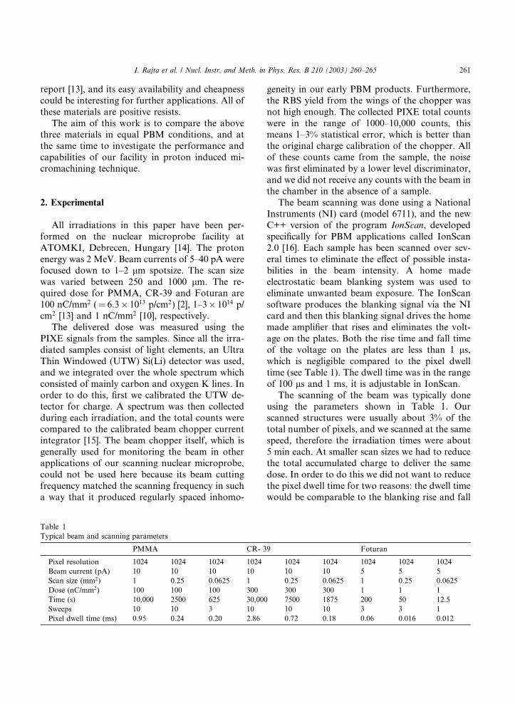
Table 1
Typical beam and scanning parameters
PMMA CR- 3
Pixel resolution 1024 1024 1024 1024
Beam current (pA) 10 10 10 10
Scan size (mm2) 1 0.25 0.0625 1
Dose (nC/mm2) 100 100 100 300
Time (s) 10,000 2500 625 30,000
Sweeps 10 10 3 10
Pixel dwell time (ms) 0.95 0.24 0.20 2.86
geneity in our early PBM products. Furthermore,
the RBS yield from the wings of the chopper was
not high enough. The collected PIXE total counts
were in the range of 1000–10,000 counts, thismeans 1–3% statistical error, which is better than
the original charge calibration of the chopper. All
of these counts came from the sample, the noise
was first eliminated by a lower level discriminator,
and we did not receive any counts with the beam in
the chamber in the absence of a sample.
The beam scanning was done using a National
Instruments (NI) card (model 6711), and the newC++ version of the program IonScan, developed
specifically for PBM applications called IonScan
2.0 [16]. Each sample has been scanned over sev-
eral times to eliminate the effect of possible insta-
bilities in the beam intensity. A home made
electrostatic beam blanking system was used to
eliminate unwanted beam exposure. The IonScan
software produces the blanking signal via the NIcard and then this blanking signal drives the home
made amplifier that rises and eliminates the volt-
age on the plates. Both the rise time and fall time
of the voltage on the plates are less than 1 ls,which is negligible compared to the pixel dwell
time (see Table 1). The dwell time was in the range
of 100 ls and 1 ms, it is adjustable in IonScan.
The scanning of the beam was typically doneusing the parameters shown in Table 1. Our
scanned structures were usually about 3% of the
total number of pixels, and we scanned at the same
speed, therefore the irradiation times were about
5 min each. At smaller scan sizes we had to reduce
the total accumulated charge to deliver the same
dose. In order to do this we did not want to reduce
the pixel dwell time for two reasons: the dwell timewould be comparable to the blanking rise and fall
9 Foturan
1024 1024 1024 1024 1024
10 10 5 5 5
0.25 0.0625 1 0.25 0.0625
300 300 1 1 1
7500 1875 200 50 12.5
10 10 3 3 1
0.72 0.18 0.06 0.016 0.012
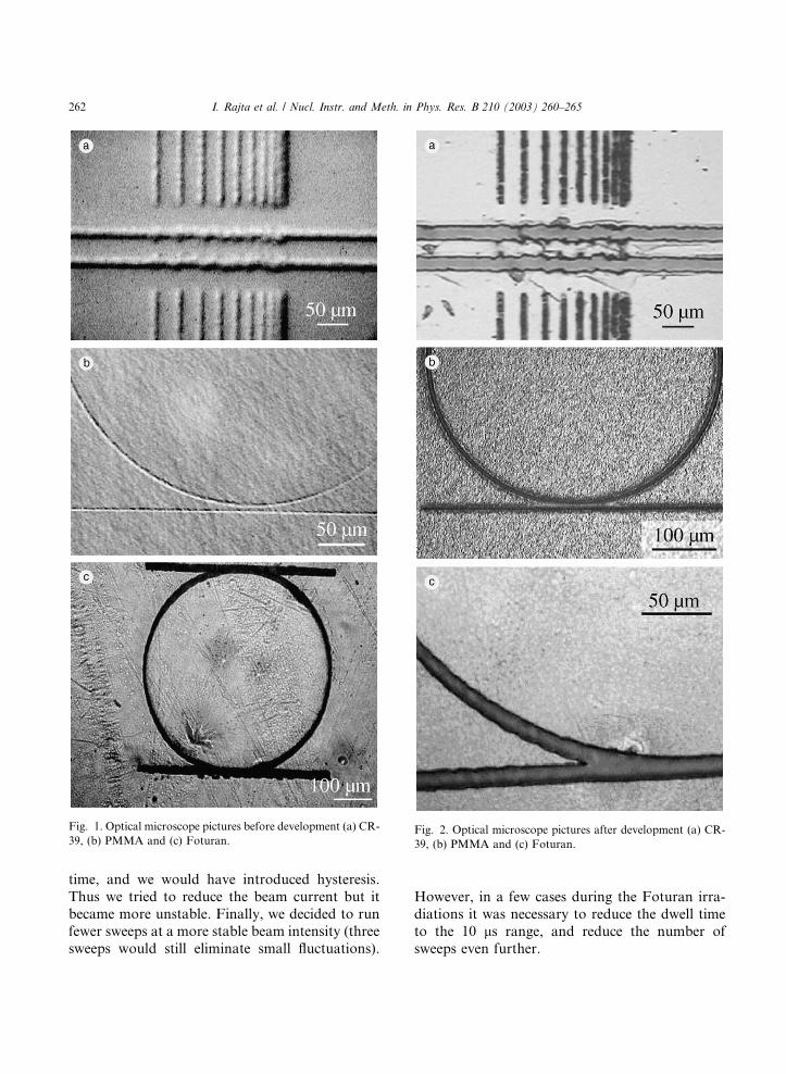
Fig. 1. Optical microscope pictures before development (a) CR-
39, (b) PMMA and (c) Foturan.Fig. 2. Optical microscope pictures after development (a) CR-
39, (b) PMMA and (c) Foturan.
262 I. Rajta et al. / Nucl. Instr. and Meth. in Phys. Res. B 210 (2003) 260–265
time, and we would have introduced hysteresis.
Thus we tried to reduce the beam current but it
became more unstable. Finally, we decided to run
fewer sweeps at a more stable beam intensity (three
sweeps would still eliminate small fluctuations).
However, in a few cases during the Foturan irra-
diations it was necessary to reduce the dwell time
to the 10 ls range, and reduce the number of
sweeps even further.

I. Rajta et al. / Nucl. Instr. and Meth. in Phys. Res. B 210 (2003) 260–265 263
After the irradiations Differential Interference
Contrast (DIC) microscopy was performed, which
is sensitive for the refractive index change in the
samples. Using this technique we were able to seethe irradiation tracks before etching. In Fig. 1
some structures are seen after irradiation but be-
fore etching, while in Fig. 2 the same structures are
shown after development.
Exposed PMMA samples were etched using the
procedure and recipe described in [2]. The proce-
dure used to develop (anneal) the Foturan glass
was the same one used in UV lithography [8], it wasthen followed by the standard etch protocol. The
CR-39 etch was done using the method that has
been routinely applied over the last 20 years of ex-
perience in the nuclear track counting technique [17].
Scanning electron microscope (SEM) images
were taken on our microstructures applying 5 kV
acceleration voltage, and secondary electron sig-
nals to generate the images. The samples were goldcoated to avoid charging.
Fig. 3. Electron microscope pictures after chemical develop-
ment (a) PMMA and (b) Foturan.
3. Results
Fig. 1(a) shows a resolution test on CR-39. The
irradiation pattern was designed to see how many
lines we can separate after irradiation, and whetherthese lines are still separated after etching. We con-
cluded that the etching process did not ruin the
structures, they were equally good quality before
and after chemical etching for CR-39 and PMMA
as well.
Fig. 1(b) shows a detail of a structure similar to
a ring resonator. The width of the gap between the
straight guide and the oval is crucial for such ap-plications. The sizes are given below (see the
comments after Fig. 2(b)).
Fig. 1(c) shows the same structure in Foturan.
The structure was not visible immediately after the
irradiation, as was the case on other samples, but
the first step of the annealing had to be done. No
chemical was used, the structure has not been
etched yet, it only changed the effective refractiveindex by forming a crystalline ceramic state at the
exposed areas, which was visible in DIC micro-
scopy. This ceramic is etched more rapidly than
the gas phase etching in hydrofluoric acid.
The pictures on Fig. 2 were taken after thechemical development on the same structures that
were shown on Fig. 1. Concerning the resolution
no differences are seen between the structures
before and after development. However there is a
difference between the resist materials PMMA
and Foturan in the case of ‘‘ring resonator’’
structure. In PMMA the straight and curved lines
are separated both before and after development.(Figs. 1(b) and 2(b)) while in Foturan they are
overlapping in both cases (Figs. 1(c) and 2(c)).
Both ‘‘ring resonator’’ structures are the same
size, but the patterns used to make them are
slightly different – the gap is 4 pixels (3.9 lmapproximately) wide in the structure made in
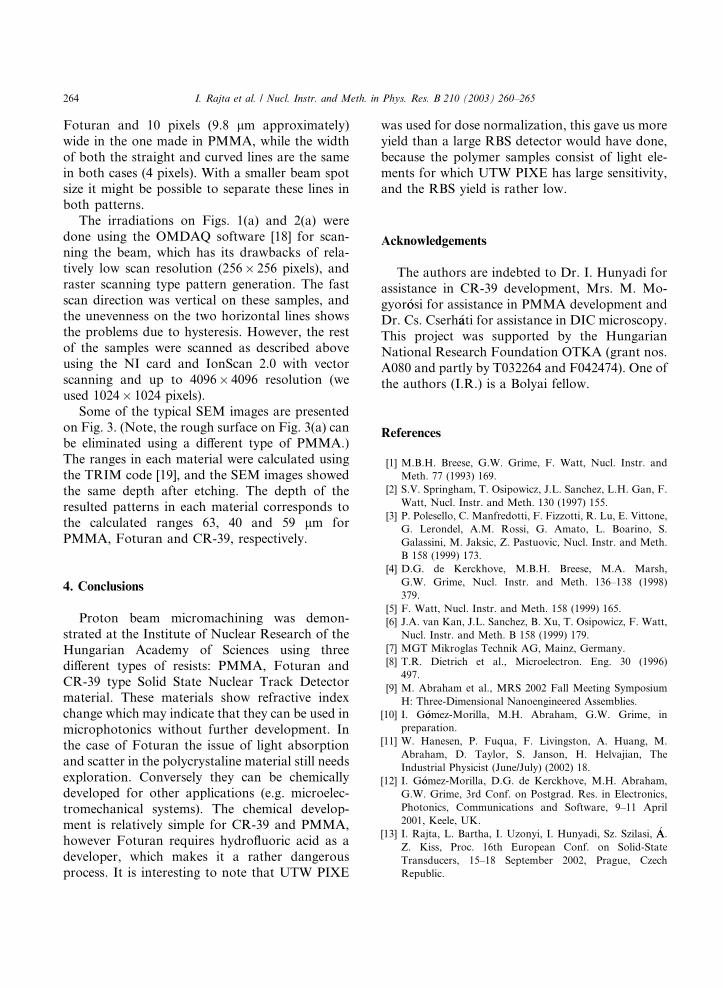
264 I. Rajta et al. / Nucl. Instr. and Meth. in Phys. Res. B 210 (2003) 260–265
Foturan and 10 pixels (9.8 lm approximately)
wide in the one made in PMMA, while the width
of both the straight and curved lines are the same
in both cases (4 pixels). With a smaller beam spotsize it might be possible to separate these lines in
both patterns.
The irradiations on Figs. 1(a) and 2(a) were
done using the OMDAQ software [18] for scan-
ning the beam, which has its drawbacks of rela-
tively low scan resolution (256� 256 pixels), and
raster scanning type pattern generation. The fast
scan direction was vertical on these samples, andthe unevenness on the two horizontal lines shows
the problems due to hysteresis. However, the rest
of the samples were scanned as described above
using the NI card and IonScan 2.0 with vector
scanning and up to 4096� 4096 resolution (we
used 1024� 1024 pixels).
Some of the typical SEM images are presented
on Fig. 3. (Note, the rough surface on Fig. 3(a) canbe eliminated using a different type of PMMA.)
The ranges in each material were calculated using
the TRIM code [19], and the SEM images showed
the same depth after etching. The depth of the
resulted patterns in each material corresponds to
the calculated ranges 63, 40 and 59 lm for
PMMA, Foturan and CR-39, respectively.
4. Conclusions
Proton beam micromachining was demon-
strated at the Institute of Nuclear Research of the
Hungarian Academy of Sciences using three
different types of resists: PMMA, Foturan and
CR-39 type Solid State Nuclear Track Detectormaterial. These materials show refractive index
change which may indicate that they can be used in
microphotonics without further development. In
the case of Foturan the issue of light absorption
and scatter in the polycrystaline material still needs
exploration. Conversely they can be chemically
developed for other applications (e.g. microelec-
tromechanical systems). The chemical develop-ment is relatively simple for CR-39 and PMMA,
however Foturan requires hydrofluoric acid as a
developer, which makes it a rather dangerous
process. It is interesting to note that UTW PIXE
was used for dose normalization, this gave us more
yield than a large RBS detector would have done,
because the polymer samples consist of light ele-
ments for which UTW PIXE has large sensitivity,and the RBS yield is rather low.
Acknowledgements
The authors are indebted to Dr. I. Hunyadi for
assistance in CR-39 development, Mrs. M. Mo-
gyor�oosi for assistance in PMMA development andDr. Cs. Cserh�aati for assistance in DIC microscopy.
This project was supported by the Hungarian
National Research Foundation OTKA (grant nos.
A080 and partly by T032264 and F042474). One of
the authors (I.R.) is a Bolyai fellow.
References
[1] M.B.H. Breese, G.W. Grime, F. Watt, Nucl. Instr. and
Meth. 77 (1993) 169.
[2] S.V. Springham, T. Osipowicz, J.L. Sanchez, L.H. Gan, F.
Watt, Nucl. Instr. and Meth. 130 (1997) 155.
[3] P. Polesello, C. Manfredotti, F. Fizzotti, R. Lu, E. Vittone,
G. Lerondel, A.M. Rossi, G. Amato, L. Boarino, S.
Galassini, M. Jaksic, Z. Pastuovic, Nucl. Instr. and Meth.
B 158 (1999) 173.
[4] D.G. de Kerckhove, M.B.H. Breese, M.A. Marsh,
G.W. Grime, Nucl. Instr. and Meth. 136–138 (1998)
379.
[5] F. Watt, Nucl. Instr. and Meth. 158 (1999) 165.
[6] J.A. van Kan, J.L. Sanchez, B. Xu, T. Osipowicz, F. Watt,
Nucl. Instr. and Meth. B 158 (1999) 179.
[7] MGT Mikroglas Technik AG, Mainz, Germany.
[8] T.R. Dietrich et al., Microelectron. Eng. 30 (1996)
497.
[9] M. Abraham et al., MRS 2002 Fall Meeting Symposium
H: Three-Dimensional Nanoengineered Assemblies.
[10] I. G�oomez-Morilla, M.H. Abraham, G.W. Grime, in
preparation.
[11] W. Hanesen, P. Fuqua, F. Livingston, A. Huang, M.
Abraham, D. Taylor, S. Janson, H. Helvajian, The
Industrial Physicist (June/July) (2002) 18.
[12] I. G�oomez-Morilla, D.G. de Kerckhove, M.H. Abraham,
G.W. Grime, 3rd Conf. on Postgrad. Res. in Electronics,
Photonics, Communications and Software, 9–11 April
2001, Keele, UK.
[13] I. Rajta, L. Bartha, I. Uzonyi, I. Hunyadi, Sz. Szilasi, �AA.
Z. Kiss, Proc. 16th European Conf. on Solid-State
Transducers, 15–18 September 2002, Prague, Czech
Republic.

I. Rajta et al. / Nucl. Instr. and Meth. in Phys. Res. B 210 (2003) 260–265 265
[14] I. Rajta, I. Borb�eely-Kiss, Gy. M�oorik, L. Bartha, E. Koltay,�AA.Z. Kiss, Nucl. Instr. and Meth. B 109–110 (1996) 148.
[15] I. Uzonyi, L. Bartha, Nucl. Instr. andMeth. 161 (2000) 339.
[16] A.A. Bettiol, J.A. van Kan, T.C. Sum, F. Watt, Nucl. Instr.
and Meth. 181 (2001) 49.
[17] Gy. Somogyi, I. Hunyadi, R. Ili�cc, A. Loose, Zs. Varga,
Nucl. Tracks Radiat. Meas. 8 (1984) 61.
[18] G.W. Grime, M. Dawson, Nucl. Instr. and Meth. B 104
(1995) 107.
[19] J.F. Ziegler, TRIM2000 private communication.