AIP/123-QED
Photon-noise limited sensitivity in titanium nitride kinetic inductance detectors
J.Hubmayr,1, a) J. Beall,1 D. Becker,1 H.-M. Cho,1, 2 M. Devlin,3 B. Dober,3 C. Groppi,4
G.C. Hilton,1 K.D. Irwin,5 D. Li,1, 2 P. Mauskopf,4 D.P. Pappas,1 J. Van Lanen,1
M.R. Vissers,1, 2 and J. Gao1, 2
1)National Institute of Standards and Technology, Boulder CO
2)University of Colorado, Boulder, CO
3)University of Pennsylvania, Department of Physics, Philadelphia,
PA
4)Arizona State University, Tempe, AZ
5)Stanford University, Palo Alto, CA
(Dated: 17 June 2014)
We demonstrate photon-noise limited performance at sub-millimeter wavelengths
in feedhorn-coupled, microwave kinetic inductance detectors (MKIDs) made of a
TiN/Ti/TiN trilayer superconducting film, tuned to have a transition temperature
of 1.4 K. The lumped-element detector design enables dual-polarization sensitivity.
The devices are fabricated on a silicon-on-insulator (SOI) wafer. Micro-machining
of the SOI wafer backside creates a quarter-wavelength backshort optimized for ef-
ficient coupling at 250 µm. Using frequency read out and when viewing a variable
temperature thermal source, we measure device noise consistent with photon noise
when the incident optical power is >1 pW, corresponding to noise equivalent powers
> 4×10⁻¹⁷ W/√
Hz. This sensitivity makes these devices suitable for broadband
photometric applications at these wavelengths.
Keywords: kinetic inductance detector, MKID, TiN, sub-millimeter, polarimeter,
photon-noise
a)Electronic mail: [email protected]
1
arX
iv:1
406.
4010
v1 [
astr
o-ph
.IM
] 1
6 Ju
n 20
14
Microwave kinetic inductance detectors (MKIDs) are superconducting pair breaking
devices1 currently in development for a broad range of applications2. Making use of high
quality factor resonators, MKIDs multiplex in the frequency domain and thus scale to
large-format arrays. MKIDs are the implemented or planned detector technology for several
sub-millimeter instruments3–7.
The fundamental limit of the sensitivity of a sub-millimeter photon integrating detector
is set by the photon fluctuations from the source under observation, which is referred to as
the photon-noise limit or background limit. The noise equivalent power (NEP) of photon
fluctuations from a narrow bandwidth source can be expressed as8
NEPphoton =√
2Phν(1 +mη). (1)
The first term describes Poisson shot noise. P is the optical power, h is Planck’s constant,
and ν is the observation center frequency. The second term describes photon bunching. m
is the occupation number per mode, and η is the efficiency from transmission to detection of
one electro-magnetic mode. MKID detectors are also limited by generation-recombination
noise9,10. In the limit of photon dominated quasiparticle production11,
NEPGR =√
2P∆/ηpb. (2)
Here ∆ is the superconducting energy gap and ηpb = 0.57 is the efficiency of converting pho-
tons to quasiparticles12. Under optical loading, generation-recombination noise is negligible
so long as ξ ≡ ∆/ηpbhν 1, which for this work ξ = 0.09.
In recent years, the sensitivity of MKIDs has increased. Photon-noise limited performance
has been achieved in aluminum MKIDs at 1.5 THz13 and 350 GHz14 at optical power levels
suitable for spectroscopy (P < 1 pW ), and at 150 GHz15 at optical powers relevant for
ground-based photometry. Photon shot noise has been detected16 at 857 GHz in devices
made of titanium nitride17 at P∼120 pW, suited to ground-based photometry.
As the superconducting material in kinetic inductance detectors, TiN has a number of
potential advantages including low loss17,18, high resistivity, large kinetic inductance fraction
and a tunable transition temperature. Recently, the spatial non-uniformity of TiN films with
Tc < 4 K has been solved by use of a new superconducting film, a TiN/Ti/TiN trilayer19.
These films show < 1% Tc variation across a 75 mm diameter wafer.
In this work, we report a measurement of photon-noise limited sensitivity in kinetic induc-
tance detectors fabricated from TiN/Ti/TiN films and at power loads relevant for balloon-
2
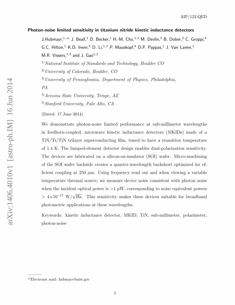
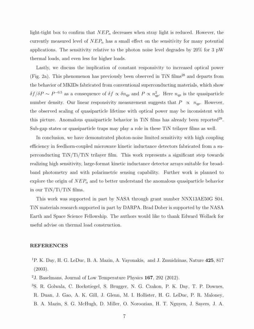
a) b)
c)
d) feedhorn
wave-‐ guide
trilayer
10 mm SOI 200 μm
Nb
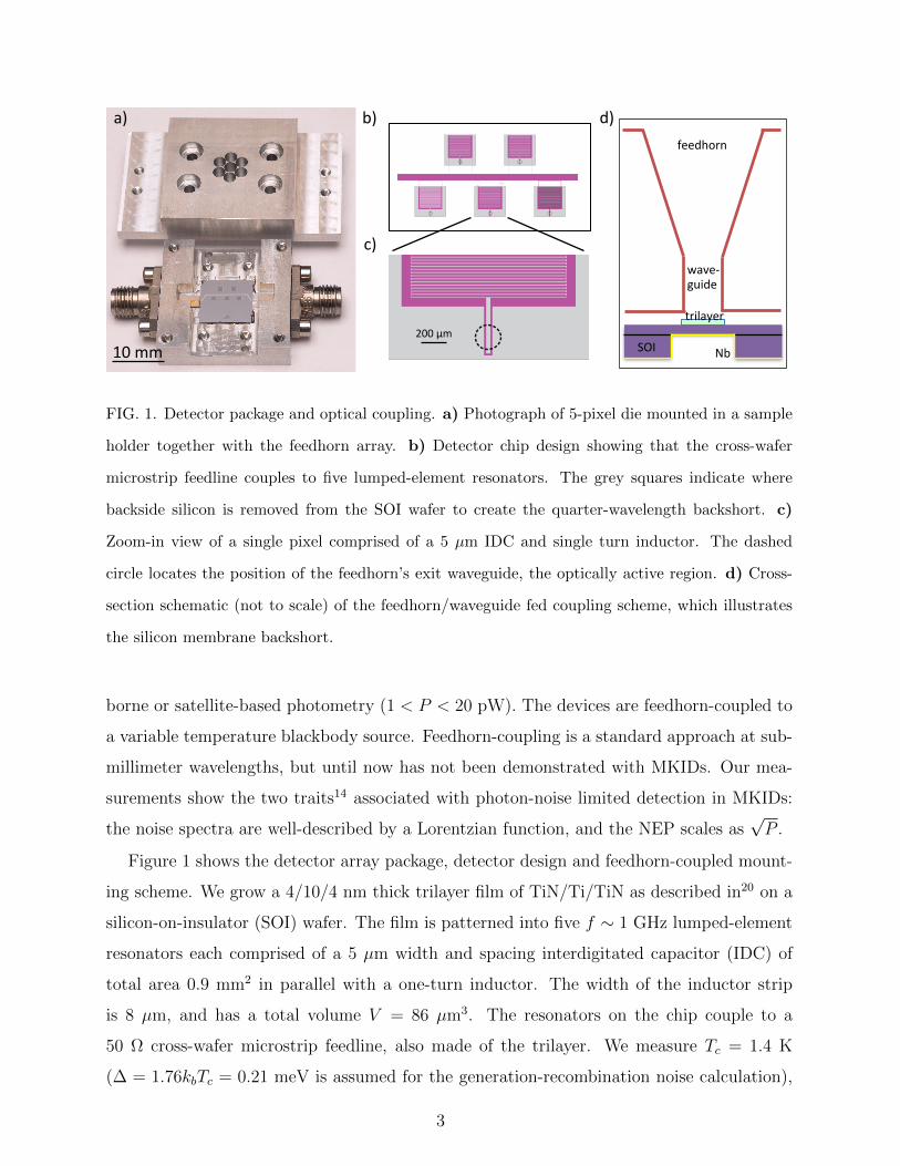
FIG. 1. Detector package and optical coupling. a) Photograph of 5-pixel die mounted in a sample
holder together with the feedhorn array. b) Detector chip design showing that the cross-wafer
microstrip feedline couples to five lumped-element resonators. The grey squares indicate where
backside silicon is removed from the SOI wafer to create the quarter-wavelength backshort. c)
Zoom-in view of a single pixel comprised of a 5 µm IDC and single turn inductor. The dashed
circle locates the position of the feedhorn’s exit waveguide, the optically active region. d) Cross-
section schematic (not to scale) of the feedhorn/waveguide fed coupling scheme, which illustrates
the silicon membrane backshort.
borne or satellite-based photometry (1 < P < 20 pW). The devices are feedhorn-coupled to
a variable temperature blackbody source. Feedhorn-coupling is a standard approach at sub-
millimeter wavelengths, but until now has not been demonstrated with MKIDs. Our mea-
surements show the two traits14 associated with photon-noise limited detection in MKIDs:
the noise spectra are well-described by a Lorentzian function, and the NEP scales as√P .
Figure 1 shows the detector array package, detector design and feedhorn-coupled mount-
ing scheme. We grow a 4/10/4 nm thick trilayer film of TiN/Ti/TiN as described in20 on a
silicon-on-insulator (SOI) wafer. The film is patterned into five f ∼ 1 GHz lumped-element
resonators each comprised of a 5 µm width and spacing interdigitated capacitor (IDC) of
total area 0.9 mm2 in parallel with a one-turn inductor. The width of the inductor strip
is 8 µm, and has a total volume V = 86 µm3. The resonators on the chip couple to a
50 Ω cross-wafer microstrip feedline, also made of the trilayer. We measure Tc = 1.4 K
(∆ = 1.76kbTc = 0.21 meV is assumed for the generation-recombination noise calculation),
3
internal quality factors of 200,000 to 400,000 at bath temperature Tbath = 75 mK, and
coupling quality factors ∼ 30,000.
The inductor element also acts as the absorber of incident sub-millimeter radiation. It is
located ∼ 50 µm below the 200 µm diameter waveguide output of the feedhorn. The sheet
impedance of the inductor is matched to the waveguide impedance and absorbs radiation
polarized along the long axis of the inductor. Future designs will include an orthogonal
MKID to achieve dual-polarization sensitivity within one spatial pixel. Modeling indicates
that dual-polarization versions of the single-polarization device tested here can be designed
to have low crosstalk, as long as the two polarization channels have widely separate resonance
frequency21. Ten micron alignment precision is set by dowel pins and machining tolerance.
To ensure high absorption efficiency, we place the absorbing inductor element at one quarter-
wavelength distance away from a backshort in silicon. The silicon behind the inductor and
capacitor is removed with deep reactive ion etch up to the buried insulator layer of the SOI
wafer. This produces a 19 µm thick silicon membrane. The oxide beneath the inductor and
capacitor is removed with a CHF3/O2 plasma etch. RF sputter deposition of a 500 nm thick
layer of Nb on the backside of the wafer creates a reflective backshort as well as a continuous
ground plane.
We mount this package to the 50 mK temperature-controlled stage of a commercial ADR
cryostat. The feedhorns view a temperature controlled THz tessellating tile22 that has
< −30 dB reflection at 600 GHz23. Using the simulated beam profile of the feedhorns, we
calculate > 99% of the optical throughput goes to the blackbody. The tile is glued into a
copper block that is weakly linked to the 3 K stage of the cryostat. We control the load
temperature between 3 K and 25 K to ∼ 1 mK stability by use of a heater and calibrated
thermometer.
The optical passband is defined by the 1 THz waveguide cut-off in the feedhorn and a
well-characterized 1.4 THz low-pass filter24 mounted to the feedhorn array. The in-band
power emitted from the load is,
P =
∫ ν2
ν1
dν( cν
)2B(ν, T )F (ν), (3)
where we have assumed the single-mode optical throughput AΩ = λ2. B(ν, T ) is the Planck
function, and F (ν) is the measured filter transmission. Metal-mesh filters are known to
have harmonic leaks at frequencies above cut-off25. However, the integrated power above the
4
0 5 10 15 20 25848.4
848.5
848.6
848.7
848.8
848.9
849
849.1
849.2
Power (pW)
f(M
Hz)
101
103
105
10−20
10−19
10−18
10−17
10−16
Frequency (Hz)
Sδf/f(H
z−1 )
10−2
10−1
100
101
102
10−16
Power (pW)
NEP
(W/√
Hz)
databest fit NEPm
NEPp hoton
21 pW7 pW1 pW
a) b) c)
FIG. 2. a) Resonant frequency versus blackbody power. b) Noise spectra for blackbody loads
between 5 K and 21 K taken at a bath temperature of 75 mK. The solid lines are fits to the
Lorentzian model described in the text. c) The blue points show the low frequency white noise
converted to a NEP via the responsivity δf/δP as a function of blackbody load. The red, dashed
line is the photon noise NEP prediction. The black, dashed line is the best fit NEP model described
in the text.
passband is < 2% of the total in-band power, even at the highest blackbody temperatures.
We perform a frequency sweep and characterize noise with a homodyne measurement and
a SiGe amplifier at thermal loads ranging from P = 5 fW to 21 pW and at Tbath = 75 mK. A
fit to the complex transmission S21(f) yields the resonant frequency as a function of thermal
power. The detector response for one device is shown in Fig. 2a. The frequency responsivity
δf/δP varies by < 10% at loading powers > 2 pW. The significance of this linearity is
discussed below.
For each thermal load, we measure noise at the microwave frequency that maximizes
δS21/δf . The approximate power on the feedline is -85 dBm, which is ∼ 13 dB below
bifurcation26,27. This choice ensures negligible non-linear effects in the resonator. We project
the raw in-phase and quadrature components of the data into the frequency and dissipation
quadratures26 and examine the noise in the frequency quadrature. Example spectra at var-
ious thermal loads are shown in Fig. 2b. Each spectrum is well described by a Lorentzian
function of white noise level A and time constant τ , associated with quasiparticle recombi-
nation, that is summed with an amplifier limiting background noise floor B,
Sδf/f (ω) =A
1 + ω2τ 2+B. (4)
The amplifier noise limit can be seen above 100 kHz. Fits to this model are shown as black
5
lines in the figure. Above 1 pW, the quasiparticle lifetime scales as τ ∼ P−0.5, as expected
in the limit of photon dominated quasiparticle generation13.
We determine the measured NEP referred to the front of the horn with a combination of
the responsivity δf/δP (slope in Fig. 2a) and the fit parameters A and B,
NEPm =
√A+B
δf/δP. (5)
These values are plotted as a function of thermal load power P in the Fig. 2c, which is the
main result of this letter. Above 1 pW the measured NEP scales as√P , demonstrating
the second signature of photon-noise limited detection in MKIDs. Furthermore, the red,
dashed line of Fig. 2c is the photon noise prediction, calculated using Eq. 1 (ν = 1.2 THz
and m < 0.1 for all blackbody temperatures). For photon loads ≥ 1 pW, the data match
the prediction indicating background limited sensitivity.
The full data set fits the model (dashed-black line of Fig. 2c)
NEP 2m = NEP 2
α +NEP 2
photon +NEP 2GR
ηopt. (6)
NEP 2α is a constant noise term that is independent of P , which we discuss below. ηopt is
the single-polarization optical efficiency, the band-averaged fraction of power detected in the
MKID that is emitted by the load. Fitting to this model has become a standard technique in
order to determine the optical efficiency of a MKID11. The fit yields ηopt = 0.97. However,
electro-magnetic simulations indicate 16% cross-polar coupling for this absorber geometry,
including a ∆z = 50 µm air gap between the absorber and waveguide. Subtracting this level
of cross-polar coupling from the fit determined ηopt yields a more reliable value of the true
single-polarization optical efficiency, ηopt = 0.81 ± 0.20. The stated error is dominated by
systematic error due in part to the uncertainty in ∆z, which changes the cross-polar coupling
prediction. This value agrees with simulations, which show 62% co-polar coupling. We note
that for future devices, we expect < 0.2% cross-polar coupling as well as improvements in
co-polar coupling by decreasing ∆z, including a waveguide choke, and decreasing the width
of the absorbing strip to 2 µm. The reduction of absorber width mandates the use of several
absorber strips in parallel to maintain the effective sheet impedance of the absorber, required
for high co-polar coupling.
At P < 1 pW, we find that the NEP saturates to NEPα = 4 × 10⁻¹⁷ W/√
Hz. Initial
measurements suggest that the source of this noise is from a background of excess quasi-
particles due to stray light absorption. We will conduct future tests in a carefully designed
6
light-tight box to confirm that NEPα decreases when stray light is reduced. However, the
currently measured level of NEPα has a small effect on the sensitivity for many potential
applications. The sensitivity relative to the photon noise level degrades by 20% for 3 pW
thermal loads, and even less for higher loads.
Lastly, we discuss the implication of constant responsivity to increased optical power
(Fig. 2a). This phenomenon has previously been observed in TiN films28 and departs from
the behavior of MKIDs fabricated from conventional superconducting materials, which show
δf/δP ∼ P−0.5 as a consequence of δf ∝ δnqp and P ∝ n2qp. Here nqp is the quasiparticle
number density. Our linear responsivity measurement suggests that P ∝ nqp. However,
the observed scaling of quasiparticle lifetime with optical power may be inconsistent with
this picture. Anomalous quasiparticle behavior in TiN films has already been reported29.
Sub-gap states or quasiparticle traps may play a role in these TiN trilayer films as well.
In conclusion, we have demonstrated photon-noise limited sensitivity with high coupling
efficiency in feedhorn-coupled microwave kinetic inductance detectors fabricated from a su-
perconducting TiN/Ti/TiN trilayer film. This work represents a significant step towards
realizing high sensitivity, large-format kinetic inductance detector arrays suitable for broad-
band photometry and with polarimetric sensing capability. Further work is planned to
explore the origin of NEPα and to better understand the anomalous quasiparticle behavior
in our TiN/Ti/TiN films.
This work was supported in part by NASA through grant number NNX13AE50G S04.
TiN materials research supported in part by DARPA. Brad Dober is supported by the NASA
Earth and Space Science Fellowship. The authors would like to thank Edward Wollack for
useful advise on thermal load construction.
REFERENCES
1P. K. Day, H. G. LeDuc, B. A. Mazin, A. Vayonakis, and J. Zmuidzinas, Nature 425, 817
(2003).
2J. Baselmans, Journal of Low Temperature Physics 167, 292 (2012).
3S. R. Golwala, C. Bockstiegel, S. Brugger, N. G. Czakon, P. K. Day, T. P. Downes,
R. Duan, J. Gao, A. K. Gill, J. Glenn, M. I. Hollister, H. G. LeDuc, P. R. Maloney,
B. A. Mazin, S. G. McHugh, D. Miller, O. Noroozian, H. T. Nguyen, J. Sayers, J. A.
7
Schlaerth, S. Siegel, A. K. Vayonakis, P. R. Wilson, and J. Zmuidzinas, in Society of Photo-
Optical Instrumentation Engineers (SPIE) Conference Series , Society of Photo-Optical
Instrumentation Engineers (SPIE) Conference Series, Vol. 8452 (2012) arXiv:1211.0595
[astro-ph.IM].
4L. J. Swenson, P. K. Day, C. D. Dowell, B. H. Eom, M. I. Hollister, R. Jarnot, A. Kovacs,
H. G. Leduc, C. M. McKenney, R. Monroe, T. Mroczkowski, H. T. Nguyen, and J. Zmuidz-
inas, in Society of Photo-Optical Instrumentation Engineers (SPIE) Conference Series ,
Society of Photo-Optical Instrumentation Engineers (SPIE) Conference Series, Vol. 8452
(2012) arXiv:1211.0315 [astro-ph.IM].
5E. Shirokoff, P. S. Barry, C. M. Bradford, G. Chattopadhyay, P. Day, S. Doyle, S. Hailey-
Dunsheath, M. I. Hollister, A. Kovacs, C. McKenney, H. G. Leduc, N. Llombart, D. P.
Marrone, P. Mauskopf, R. O’Brient, S. Padin, T. Reck, L. J. Swenson, and J. Zmuidzinas,
in Society of Photo-Optical Instrumentation Engineers (SPIE) Conference Series , Society
of Photo-Optical Instrumentation Engineers (SPIE) Conference Series, Vol. 8452 (2012)
arXiv:1211.1652 [astro-ph.IM].
6A. Monfardini, R. Adam, A. Adane, P. Ade, P. Andre, A. Beelen, B. Belier, A. Benoit,
A. Bideaud, N. Billot, O. Bourrion, M. Calvo, A. Catalano, G. Coiffard, B. Comis,
A. D’Addabbo, F.-X. Desert, S. Doyle, J. Goupy, C. Kramer, S. Leclercq, J. Macias-
Perez, J. Martino, P. Mauskopf, F. Mayet, F. Pajot, E. Pascale, N. Ponthieu, V. Reveret,
L. Rodriguez, G. Savini, K. Schuster, A. Sievers, C. Tucker, and R. Zylka, Journal of Low
Temperature Physics (2013), 10.1007/s10909-013-0985-4, arXiv:1310.1230 [astro-ph.IM].
7J. Hubmayr, J. Beall, D. Becker, J. Brevik, H. Cho, G. Che, M. Devlin, B. Dober, J. Gao,
N. Galitzki, et al., Journal of Low Temperature Physics (2014).
8J. Zmuidzinas, Applied Optics 42, 4989 (2003).
9P. J. de Visser, J. J. A. Baselmans, P. Diener, S. J. C. Yates, A. Endo, and T. M. Klapwijk,
Physical Review Letters 106, 167004 (2011), arXiv:1103.0758 [cond-mat.supr-con].
10C. Wilson, L. Frunzio, and D. Prober, Physical Review Letters 87, 067004 (2001).
11S. J. C. Yates, J. J. A. Baselmans, A. Endo, R. M. J. Janssen, L. Ferrari, P. Diener, and
A. M. Baryshev, Applied Physics Letters 99, 073505 (2011).
12A. G. Kozorezov, A. F. Volkov, J. K. Wigmore, A. Peacock, A. Poelaert, and R. den
Hartog, Phys. Rev. B 61, 11807 (2000).
13P. J. de Visser, J. J. A. Baselmans, J. Bueno, N. Llombart, and T. M. Klapwijk, Nature
8
Communications 5, 3130 (2014), 10.1038/ncomms4130, arXiv:1306.4238 [cond-mat.supr-
con].
14R. M. J. Janssen, J. J. A. Baselmans, A. Endo, L. Ferrari, S. J. C. Yates, A. M. Bary-
shev, and T. M. Klapwijk, Applied Physics Letters 103, 203503 (2013), arXiv:1311.2429
[physics.ins-det].
15P. Mauskopf, S. Doyle, P. Barry, S. Rowe, A. Bidead, P. Ade, C. Tucker, E. Castillo,
A. Monfardini, J. Goupy, et al., Journal of Low Temperature Physics (2014).
16C. M. McKenney, H. G. Leduc, L. J. Swenson, P. K. Day, B. H. Eom, and J. Zmuidzinas,
in Society of Photo-Optical Instrumentation Engineers (SPIE) Conference Series , Society
of Photo-Optical Instrumentation Engineers (SPIE) Conference Series, Vol. 8452 (2012).
17H. G. Leduc, B. Bumble, P. K. Day, B. H. Eom, J. Gao, S. Golwala, B. A. Mazin,
S. McHugh, A. Merrill, D. C. Moore, O. Noroozian, A. D. Turner, and J. Zmuidzinas,
Applied Physics Letters 97, 102509 (2010), arXiv:1003.5584 [cond-mat.supr-con].
18M. R. Vissers, J. Gao, D. S. Wisbey, D. A. Hite, C. C. Tsuei, A. D. Corcoles, M. Steffen,
and D. P. Pappas, Applied Physics Letters 97, 232509 (2010).
19M. R. Vissers, J. Gao, J. S. Kline, M. Sandberg, M. P. Weides, D. S. Wisbey, and D. P.
Pappas, Thin Solid Films 548, 485 (2013), arXiv:1209.4626 [cond-mat.supr-con].
20M. R. Vissers, J. Gao, M. Sandberg, S. M. Duff, D. S. Wisbey, K. D. Irwin, and D. P.
Pappas, Applied Physics Letters 102, 232603 (2013), arXiv:1209.4853 [cond-mat.supr-con].
21J. Hubmayr, J. Beall, D. Becker, H. Cho, B. Dober, M. Devlin, A. Fox, J. Gao, G. Hilton,
K. Irwin, et al., Applied Superconductivity, IEEE Transactions on 23, 2400304 (2013).
22T. K. Instruments, “http://www.terahertz.co.uk,” Such identification does not imply rec-
ommendation or endorsement by the National Institute of Standards and Technology, nor
does it imply that the materials or equipment identified are necessarily the best available
for the purpose.
23J. Saily and A. V. Raisanen, Studies on Specular and Non-specular Reflectivities of Radar
Absorbing Materials (RAM) at Submillimetre Wavelengths, Tech. Rep. Report S 258
(Helsinki University of Technology Department of Electrical and Communications En-
gineering Radio Laboratory, 2003).
24E. Pascale, P. A. R. Ade, J. J. Bock, E. L. Chapin, J. Chung, M. J. Devlin, S. Dicker,
M. Griffin, J. O. Gundersen, M. Halpern, P. C. Hargrave, D. H. Hughes, J. Klein, C. J.
MacTavish, G. Marsden, P. G. Martin, T. G. Martin, P. Mauskopf, C. B. Netterfield,
9
L. Olmi, G. Patanchon, M. Rex, D. Scott, C. Semisch, N. Thomas, M. D. P. Truch,
C. Tucker, G. S. Tucker, M. P. Viero, and D. V. Wiebe, Astrophysical Journal 681, 400
(2008), arXiv:0711.3465.
25P. A. R. Ade, G. Pisano, C. Tucker, and S. Weaver, in Society of Photo-Optical Instru-
mentation Engineers (SPIE) Conference Series , Society of Photo-Optical Instrumentation
Engineers (SPIE) Conference Series, Vol. 6275 (2006).
26J. Zmuidzinas, Annual Review of Condensed Matter Physics 3, 169 (2012),
http://www.annualreviews.org/doi/pdf/10.1146/annurev-conmatphys-020911-125022.
27L. J. Swenson, P. K. Day, B. H. Eom, H. G. Leduc, N. Llombart, C. M. McKen-
ney, O. Noroozian, and J. Zmuidzinas, Journal of Applied Physics 113, 104501 (2013),
arXiv:1305.4281 [cond-mat.supr-con].
28O. Noroozian, Superconducting Microwave Resonator Arrays for Submillimeter/Far-
Infrared Imaging, Ph.D. thesis, California Institute of Technology (2012).
29J. Gao, M. R. Vissers, M. O. Sandberg, F. C. S. da Silva, S. W. Nam, D. P. Pappas, D. S.
Wisbey, E. C. Langman, S. R. Meeker, B. A. Mazin, H. G. Leduc, J. Zmuidzinas, and
K. D. Irwin, Applied Physics Letters 101, 142602 (2012), arXiv:1208.0871 [cond-mat.supr-
con].
10