NEGF SIMULATION OF ELECTRON TRANSPORT IN RESONANT
TUNNELING AND RESONANT INTERBAND TUNNELING DIODES
A Thesis
Submitted to the Faculty
of
Purdue University
by
Arun Goud Akkala
In Partial Fulfillment of the
Requirements for the Degree
of
Master of Science in Electrical and Computer Engineering
December 2011
Purdue University
West Lafayette, Indiana

ii
To my family...
iii
ACKNOWLEDGMENTS
I’m grateful to my advisor prof. Gerhard Klimeck for giving me the opportunity
to be his student and conduct research in his group. His encouragement as well as
criticism have been a strong motivation for me to try harder and come up with my
best.
I also wish to thank prof. Mark Lundstrom and prof. Vladimir Shalaev for their
role as my advisory committee members. Prof. Lundstrom’s excellent tutorship in
ECE 606 Solid State Devices was the key in inspiring me to pursue this track. There
were times when ploughing through the vast literature and the complex numerical
techniques employed in device modeling left me feeling lost. In times like these,
prof. Datta’s brilliant lectures hosted on Nanohub often came to my rescue. I also
acknowledge his great patience and willingness to answer questions I had during
ECE 495 and 659 class hours, two courses that undoubtedly raised my awareness of
Quantum effects and transport in Nanoelectronic Devices.
Most of the projects that I was involved with used the atomistic simulation tool
NEMO5. The developers Sebastian Steiger, Hong-Hyun Park, Tillmann Kubis and
Michael Povolotskyi offered tremendous support to me in helping understand the
various solvers built into NEMO5. The time spent on the 1dhetero, Brillouin zone
viewer tool with Sebastian and RTD NEGF with Hong-Hyun and Zhengping were
particularly the most fruitful to me in terms of learning about numerical techniques
used in device modeling.
The weekly group meetings and presentations by my fellow group members taught
me some of the challenges of device modelling and effective presentation of research
work. There are too many students to be named here, so instead I’ll thank them
collectively and wish them the best for their respective degrees.

iv
I’ve enjoyed being a contributor to NanoHUB, using its simulation tools for home-
work and going through its treasure trove of educational resources. NanoHUB’s ad-
ministrator Steven Clark and Rappture support team consisting of Derrick Kearney
and George Howlett were quick to answer questions relating to tool installation on
Nanohub and other computational issues I came across. I express my gratitude to
them as well as to NCN, RCAC for the computational resources and to Vicki Johnson
and Cheryl Haines for help with scheduling appointments. Special thanks is also due
to Xufeng Wang who shared his prior experience working with Rappture when I was
stuck on the Brillouin zone viewer tool development and for sharing his custom TCL
shell code that went into the 1dhetero tool’s code.
Lastly, it would be unfair if I didn’t thank my parents and my sister for their
support when my morale was down. They always stood by my side and encouraged
me to pursue what I wanted to. I’m indebted to them for their belief in my abilities...

v
TABLE OF CONTENTS
Page
LIST OF TABLES . . . . . . . . . . . . . . . . . . . . . . . . . . . . . . . . viii
LIST OF FIGURES . . . . . . . . . . . . . . . . . . . . . . . . . . . . . . . ix
ABBREVIATIONS . . . . . . . . . . . . . . . . . . . . . . . . . . . . . . . . xiii
NOMENCLATURE . . . . . . . . . . . . . . . . . . . . . . . . . . . . . . . xiv
ABSTRACT . . . . . . . . . . . . . . . . . . . . . . . . . . . . . . . . . . . xv
1 INTRODUCTION . . . . . . . . . . . . . . . . . . . . . . . . . . . . . . 1
1.1 Beyond Si CMOS . . . . . . . . . . . . . . . . . . . . . . . . . . . . 1
1.2 RTDs for digital logic and memory circuits . . . . . . . . . . . . . . 2
1.3 Motivation for studying RTDs . . . . . . . . . . . . . . . . . . . . . 4
1.4 Computational Modeling of RTDs . . . . . . . . . . . . . . . . . . . 5
1.5 Need for Atomistic Device Simulation . . . . . . . . . . . . . . . . . 5
1.6 Outline . . . . . . . . . . . . . . . . . . . . . . . . . . . . . . . . . . 6
2 PHYSICS OF RTDS . . . . . . . . . . . . . . . . . . . . . . . . . . . . . 8
2.1 Introduction . . . . . . . . . . . . . . . . . . . . . . . . . . . . . . . 8
2.2 Structure of a GaAs/AlGaAs RTD . . . . . . . . . . . . . . . . . . 8
2.3 Quasi-bound states and resonant transmission . . . . . . . . . . . . 9
2.4 Global coherent tunneling . . . . . . . . . . . . . . . . . . . . . . . 11
2.5 Tunneling current density . . . . . . . . . . . . . . . . . . . . . . . 11
2.6 Transfer matrix method . . . . . . . . . . . . . . . . . . . . . . . . 15
2.7 Esaki-Tsu Current formula . . . . . . . . . . . . . . . . . . . . . . . 17
2.8 Valley current . . . . . . . . . . . . . . . . . . . . . . . . . . . . . . 17
2.8.1 Minimizing thermionic emission current . . . . . . . . . . . . 18
2.8.2 Minimizing current due to higher resonances . . . . . . . . . 18
2.8.3 Effect of scattering . . . . . . . . . . . . . . . . . . . . . . . 18

vi
Page
3 MODELING OF RTDS IN RTD NEGF . . . . . . . . . . . . . . . . . . 21
3.1 Intoduction . . . . . . . . . . . . . . . . . . . . . . . . . . . . . . . 21
3.2 Electrostatics . . . . . . . . . . . . . . . . . . . . . . . . . . . . . . 21
3.2.1 Thomas-Fermi Model (Semiclassical treatment) . . . . . . . 21
3.2.2 Hartree Model (Quantum Mechanical treatment) . . . . . . 24
3.3 Transport . . . . . . . . . . . . . . . . . . . . . . . . . . . . . . . . 32
3.3.1 Transmission and Current . . . . . . . . . . . . . . . . . . . 32
3.4 Self-consistent electrostatic potential calculation . . . . . . . . . . . 33
3.5 Thomas-Fermi vs Hartree method . . . . . . . . . . . . . . . . . . . 35
3.5.1 Conduction band profile . . . . . . . . . . . . . . . . . . . . 35
3.5.2 Free charge density . . . . . . . . . . . . . . . . . . . . . . . 36
3.5.3 Current . . . . . . . . . . . . . . . . . . . . . . . . . . . . . 40
3.6 Cumulative current density . . . . . . . . . . . . . . . . . . . . . . . 43
3.7 2D-2D Tunneling . . . . . . . . . . . . . . . . . . . . . . . . . . . . 45
3.8 Summary . . . . . . . . . . . . . . . . . . . . . . . . . . . . . . . . 46
4 RESONANT INTERBAND TUNNELING DIODES . . . . . . . . . . . . 47
4.1 Introduction . . . . . . . . . . . . . . . . . . . . . . . . . . . . . . . 47
4.2 Esaki diode . . . . . . . . . . . . . . . . . . . . . . . . . . . . . . . 47
4.3 InAs/AlSb/GaSb RITD . . . . . . . . . . . . . . . . . . . . . . . . 49
4.4 Multiband modeling . . . . . . . . . . . . . . . . . . . . . . . . . . 52
4.5 Current density . . . . . . . . . . . . . . . . . . . . . . . . . . . . . 53
4.6 Simulation Results . . . . . . . . . . . . . . . . . . . . . . . . . . . 53
4.6.1 IV characteristics . . . . . . . . . . . . . . . . . . . . . . . . 53
4.6.2 At peak and valley voltage . . . . . . . . . . . . . . . . . . . 55
4.6.3 At high bias (1.1V) . . . . . . . . . . . . . . . . . . . . . . . 61
4.7 Applications . . . . . . . . . . . . . . . . . . . . . . . . . . . . . . . 63
4.8 Summary . . . . . . . . . . . . . . . . . . . . . . . . . . . . . . . . 63
5 1DHETERO AND BRILLOUIN ZONE VIEWER . . . . . . . . . . . . . 64

vii
Page
5.1 1dhetero tool . . . . . . . . . . . . . . . . . . . . . . . . . . . . . . 64
5.2 Brillouin Zone Viewer tool . . . . . . . . . . . . . . . . . . . . . . . 70
6 SUMMARY . . . . . . . . . . . . . . . . . . . . . . . . . . . . . . . . . . 72
LIST OF REFERENCES . . . . . . . . . . . . . . . . . . . . . . . . . . . . 74
APPENDIX . . . . . . . . . . . . . . . . . . . . . . . . . . . . . . . . . . . . 76
A RTD NEGF - USER OPTIONS . . . . . . . . . . . . . . . . . . . . . . . 76
A.1 Basic options . . . . . . . . . . . . . . . . . . . . . . . . . . . . . . 76
A.2 Multiscale Domains options . . . . . . . . . . . . . . . . . . . . . . 78
A.3 Advanced options . . . . . . . . . . . . . . . . . . . . . . . . . . . . 78
A.4 Resonance Finder options . . . . . . . . . . . . . . . . . . . . . . . 80

viii
LIST OF TABLES
Table Page
3.1 GaAs/AlGaAs DBRTD structure used in the simulations. . . . . . . . 35
3.2 Simulation parameters for GaAs/AlGaAs DBRTD structure used in thesimulations. . . . . . . . . . . . . . . . . . . . . . . . . . . . . . . . . . 36
4.1 InAs/AlSb/GaSb RITD structure used in the simulations. . . . . . . . 54
5.1 Substrates and materials supported by 1dheterostructure tool . . . . . 64

ix
LIST OF FIGURES
Figure Page
1.1 Simulated current voltage characteristics at 300K of a GaAs/AlGaAs RTDstructure (used in Chapter 3) showing negative differential resistance. 2
1.2 A 6 transistor SRAM memory cell (top), an RTD latch based SRAMmemory cell (bottom, left) and its load line diagram (bottom, right) [4],[5]. . . . . . . . . . . . . . . . . . . . . . . . . . . . . . . . . . . . . . 3
2.1 Conduction band diagram (at Γ point) for a GaAs/AlGaAs DBRTD underequilibrium . . . . . . . . . . . . . . . . . . . . . . . . . . . . . . . . . 8
2.2 Quasi Bound states of a quantum well . . . . . . . . . . . . . . . . . . 10
2.3 The transmission coefficient plot shows peaks at energies equal to the quasibound state energies of the GaAs quantum well. . . . . . . . . . . . . 10
2.4 Current voltage characteristics when Eo >> EF in emitter and when nobias is applied. . . . . . . . . . . . . . . . . . . . . . . . . . . . . . . . 12
2.5 Current voltage characteristics when Ec < Eo < EF in emitter, i.e., ap-plied bias is smaller than peak voltage. . . . . . . . . . . . . . . . . . 13
2.6 Current voltage characteristics when Eo = Ec in emitter,i.e., when appliedbias is equal to the peak voltage. . . . . . . . . . . . . . . . . . . . . . 14
2.7 Expected IV characteristics at 0K . . . . . . . . . . . . . . . . . . . . 14
2.8 Small potential steps are used for Transfer matrix calculation. . . . . . 15
3.1 Partitioning of regions for semiclassical simulation. The charge density inthe well is set to 0. The potential variation is therefore linear in the well. 23
3.2 Simulation flow for semiclassical Thomas-Fermi simulation for one biasvoltage value. . . . . . . . . . . . . . . . . . . . . . . . . . . . . . . . . 23
3.3 Quantum modeling of regions. . . . . . . . . . . . . . . . . . . . . . . . 25
3.4 Computation of left connected Green’s function and fully connected Green’sfunction. . . . . . . . . . . . . . . . . . . . . . . . . . . . . . . . . . . . 29
3.5 Simulation flow for Hartree self-consistent simulation for one bias voltagevalue. . . . . . . . . . . . . . . . . . . . . . . . . . . . . . . . . . . . . 34

x
Figure Page
3.6 Conduction band edge profile obtained from semiclassical Thomas Fermimodel (blue) and Hartree quantum self-consistent method (red). The up-ward shift for the Hartree result in the well region is due to the presenceof charge in the well which pulls the conduction band edge and the reso-nance level upwards in energy as against the applied bias which tries topull them down . . . . . . . . . . . . . . . . . . . . . . . . . . . . . . . 37
3.7 Comparison of electron density obtained from a Thomas-Fermi and Hartreequantum self-consistent caclculations for different bias voltages applied tothe DBRTD. The 2nd plot is at peak voltage Vc = 0.2V . . . . . . . . 39
3.8 IV characteristics computed from semiclassical Thomas Fermi model (blue)and Hartree quantum self-consistent method (red) . . . . . . . . . . . . 40
3.9 Variation of first 2 resonances (in red) for Thomas-Fermi (left) and Hartreequantum self-consistent (right) methods. The emitter Fermi level (inblue), the conduction band edge at the left spacer/barrier interface (bot-tom black line) and the peak conduction band edge to the left of the barrier(top black line) are also shown. . . . . . . . . . . . . . . . . . . . . . . 41
3.10 Conduction band edge profile (top), quantum charge density (center, blue)at 0.475 V and variation of quantum charge (bottom, orange), semiclassicalcharge (bottom, red) with bias in the non-equilibrium device region. Asthe 2nd barrier becomes shorter with bias, the well charge diminishes. 42
3.11 Conduction band profile (left),transmission coefficient (center,blue), cur-rent density (center, dark green), normalized cumulative current density(center, light green) and resonance energy vs voltage at peak voltage of0.2V. The normalized cumulative current density shows that the 1st reso-nance level is the major contributor to the total current. . . . . . . . . 43
3.12 Conduction band profile (left),transmission coefficient (center,blue), cur-rent density (center, dark green), normalized cumulative current density(center, light green) and IV curve at a voltage of 0.375V. The normalizedcumulative current density shows that the 1st resonance level is no longercontributing significantly to the total current. . . . . . . . . . . . . . . 44
3.13 Emitter quasi-bound state (left, orange) at an applied bias of 0.68V. Tun-neling from this quasi-bound state into well resonance contributes somecurrent although its magnitude is much smaller than the current arisingfrom the higher order well resonance. . . . . . . . . . . . . . . . . . . 45
4.1 Esaki diode operation. . . . . . . . . . . . . . . . . . . . . . . . . . . . 48
4.2 Equilibrium band diagram for an InAs/AlSb/GaSb RITD. . . . . . . . 49

xi
Figure Page
4.3 Equilibrium band diagram and overlap between InAs emitter bands andGaSb valence subband dispersions along kx for an InAs/AlSb/GaSb RITD. 51
4.4 Band diagram for voltages greater than peak voltage and overlap betweenInAs emitter bands and GaSb valence subband dispersions along kx for anInAs/AlSb/GaSb RITD. . . . . . . . . . . . . . . . . . . . . . . . . . 51
4.5 IV curve for the InAs/AlSb/GaSb RITD at 300K showing a PVR of 50. 54
4.6 Energy integrated current density J(kx, ky) along kx direction at peakvoltage (top) and at valley voltage (bottom). . . . . . . . . . . . . . . 56
4.7 Energy integrated current density J(kx, ky) along ky direction at peakvoltage (top) and at valley voltage (bottom). . . . . . . . . . . . . . . 57
4.8 Energy integrated current density J(kx, ky) along kx = ky direction atpeak voltage (top) and at valley voltage (bottom). . . . . . . . . . . . 58
4.9 Cumulative current density along ky = 0 at peak voltage (top) and atvalley voltage (bottom). . . . . . . . . . . . . . . . . . . . . . . . . . . 59
4.10 LDOS profile along with current density plot for ky = 0 direction showingthe energy at which the current is flowing for peak voltage (top) and atvalley voltage (bottom). . . . . . . . . . . . . . . . . . . . . . . . . . . 60
4.11 LDOS and current density at 1.1V. . . . . . . . . . . . . . . . . . . . . 61
4.12 LDOS and current density at 1.1V. . . . . . . . . . . . . . . . . . . . . 62
5.1 Design section of the 1dhetero tool where the dimensions and doping den-sity of the materials and substrate constituing the heterostructure can bespecified. . . . . . . . . . . . . . . . . . . . . . . . . . . . . . . . . . . . 67
5.2 Equilibrium conduction band profile and bound state resonances for thedefault AlGaAs/GaAs heterostructure calculated from a single band sim-ulation. . . . . . . . . . . . . . . . . . . . . . . . . . . . . . . . . . . . 68
5.3 Equilibrium potential profile for the default AlGaAs/GaAs heterostructurecalculated from a single band simulation. The potential peak is due todepletion of carriers in the doped AlGaAs barrier. . . . . . . . . . . . . 68
5.4 Equilibrium sheet density profile for the default AlGaAs/GaAs heterostruc-ture calculated from a single band simulation. A 2DEG is formed near theAlGaAs-GaAs interface resulting in a very high sheet concentration of8.8× 1012/cm2. . . . . . . . . . . . . . . . . . . . . . . . . . . . . . . . 69

xii
Figure Page
5.5 Equilibrium sheet density profile for the default AlGaAs/GaAs heterostruc-ture calculated from a semiclassical Thomas-Fermi simulation. The semi-classical method predicts maximum sheet density at the AlGaAs-GaAsinterface whereas the single band calculation result of Fig.5.4 shows max-imum sheet concentration at the center of the inversion layer, away fromthe AlGaAs-GaAs interface. . . . . . . . . . . . . . . . . . . . . . . . . 69
5.6 Brillouin zone viewer tool showing the 1st Brillouin zone for the cubicFCC lattice. . . . . . . . . . . . . . . . . . . . . . . . . . . . . . . . . 71
A.1 RTD NEGF simulation tool showing Basic tab options. . . . . . . . . 77
A.2 Multiscale Domains tab options. . . . . . . . . . . . . . . . . . . . . . 78
A.3 Advanced tab options. . . . . . . . . . . . . . . . . . . . . . . . . . . . 79
A.4 Resonance Finder tab options. . . . . . . . . . . . . . . . . . . . . . . 80

xiii
ABBREVIATIONS
RTD Resonant tunneling diode
RITD Resonant interband tunneling diode
DBRTD Double barrier resonant tunneling diode
NEGF Non-equilibrium Green’s function
MBE Molecular beam epitaxy
MOCVD Metal organic chemical vapour deposition
LDOS Local density of states
EMA Effective mass approximation
PVR Peak to valley current ratio
IV Current voltage characteristics
NDR Negative differential resistance
NEMO5 NanoElectronic MOdeling program

xiv
NOMENCLATURE
GaAs Gallium Arsenide
AlGaAs Aluminium Gallium Arsenide
AlAs Aluminium Arsenide
InAs Indium Arsenide
GaSb Gallium Antimonide
AlSb Aluminium Antimonide
InGaAs Indium Gallium Arsenide
InAlAs Indium Aluminium Arsenide
InP Indium Phosphide
GaP Gallium Phosphide
AlP Aluminium Phosphide
Si Silicon
Ge Germanium
SiO2 Silicon Dioxide

xv
ABSTRACT
Akkala, Arun Goud M.S.E.C.E., Purdue University, December 2011. NEGF Simula-tion of Electron Transport in Resonant Tunneling and Resonant Interband TunnelingDiodes. Major Professor: Gerhard Klimeck.
The challenges due to continuous scaling of CMOS has prompted research into
alternative structures for future logic devices that are capable of high speed opera-
tion with reduced power consumption. One such contender in the emerging devices
category, the Resonant tunneling diode (RTD), has attracted considerable interest
due to its low voltage operation, THz capabilities and negative differential resistance.
RTDs operate on the principle of quantum mechanical tunneling of electrons through
a potential barrier into quantized well states resulting in resonances in the transmis-
sion characteristics. Due to the quantum mechanical nature of the tunneling process,
quantum transport simulation models are needed to describe RTD characteristics. In
this work, a simulation tool based on the Non-Equilibrium Green’s Function formal-
ism using effective mass approach has been developed to study GaAs/AlGaAs RTD
characteristics. Scattering in the emitter reservoir has been treated in an approximate
manner to ease computational burden.
However the room temperature peak to valley current ratio (PVR), which is the
figure of merit for RTDs, has to be improved in order to make them a suitable
candidate for digital applications. Resonant Interband Tunneling diodes (RITD) are
capable of achieving higher PVRs by reducing valley current. A multiband model is
required for RITDs since both conduction and valence band play a role. An sp3s*
spin-orbit based tight binding model along with an NEGF based transport solver has
been used to study a coherent InAs/AlSb/GaSb RITD and the simulated IV shows
a high PVR of 50.

1
1. INTRODUCTION
1.1 Beyond Si CMOS
Silicon based CMOS has been the dominant technology of the semiconductor
industry for the last 50 years. The chip density and operating speed of Si based
ICs have shown a regular trend of growth while the operating voltage has steadily
decreased over the past decades. This has been achieved through continuous scaling
of transistor dimensions. However as dimensions approach close to the wavelength of
an electron, quantum effects such as tunneling, interference, quantization that arise
due to wave nature of electron start playing an important role in determining device
performance.
Novel devices with a different operational paradigm over conventional field effect
based devices can be built by utilizing these quantum mechanical effects. With the
help of high mobility III-V compound semiconductors and advances in heteroepitax-
ial growth techniques such as Molecular Beam Epitaxy (MBE) and Metal-Organic
Chemical Vapour Deposition, it has become possible to realize devices with very fast
switching speeds and that are also capable of operating at low voltages, two very
critical requirements for future digital logic technologies. Resonant tunneling diodes
(RTD) hold a lot of promise in this regard. The negative differential resistance (NDR)
characteristics exhibited by RTDs due to the resonant tunneling phenomenon have
resulted in their usage in some niche applications. Since 1974, when the first GaAs-
AlGaAs based RTD was demonstrated by Chang, Esaki and Tsu, [1] RTDs have
been explored as alternatives to transistors for high frequency applications [2] such
as microwave circuits and even logic circuits [3].

2
Fig. 1.1. Simulated current voltage characteristics at 300K of aGaAs/AlGaAs RTD structure (used in Chapter 3) showing negativedifferential resistance.
1.2 RTDs for digital logic and memory circuits
The ultra high speed capabilities and low voltage operation of RTDs make them
a suitable future choice for digital logic devices. RTDs are considered as multi-
functional devices in that operations and functionalities that could be realized using
conventional techniques such as using transistors can be implemented differently using
RTDs and usually using fewer number of components. For instance Fig.1.2 depicts
a conventional 6 transistor SRAM memory cell which consists of 2 cross-coupled
inverters that acts as a latch to store data indefinitely. The same latching operation
can be implemented using 2 series connected RTDs as is clear from the load line
characteristics [4], [5].

3
Fig. 1.2. A 6 transistor SRAM memory cell (top), an RTD latch basedSRAM memory cell (bottom, left) and its load line diagram (bottom,right) [4], [5].

4
There are 3 operating points of which only A and B are stable. A can be treated
as the logic LOW state and B the logic HIGH state. By thus implementing the SRAM
function using RTDs, a significant reduction in the total size of the chip is possible.
More importantly, scaling of transistors to nanometer regime results in undesirable
effects such as leakage currents but for resonant tunneling to occur, RTDs require
dimensions that are already in the nanometer regime and are therefore conducive for
development of memory and even logic circuits with reduced areas.
1.3 Motivation for studying RTDs
Despite the high speed and low voltage operation advantages offered by RTDs
there are some drawbacks too due to which RTDs have not become widespread.
These are
1. RTDs are 2 terminal devices and cannot offer input to output isolation. They
can therefore only augment transistors but cannot replace them.
2. The load driving capabilities of RTDs are poor and hence overall throughput
would be affected. To increase the drive capabilities of RTDs, the peak current
and the PVR need to be improved.
3. The most critical shortcoming is that RTDs with excellent PVRs can be grown
using GaAs/AlGaAs, InGaAs/InAlAs and other III-V compound semiconduc-
tors all of which are incompatible with the mainstream Si technology and are
expensive to manufacture. Si/SiGe RTDs that are compatible with Si technol-
ogy have been demonstrated but they tend to have low PVRs due to the short
barrier height of SiGe.
So far, RTDs have been commonly used alongside III-V based HEMTs [6]. But
as advances in fabrication techniques such as MBE continue, in the near future, we
may have a viable and inexpensive way of manufacturing RTDs and integrating them
with Si based circuits as well as III-V based HEMTs.

5
The immediate goal then is to understand and develop simulation models that
can capture the underlying Physics of operation of RTDs accurately. Beginning with
simple approximations, the models are then refined to account for effects happening
in realistic devices such as scattering thereby giving us a better understanding and a
deeper insight into RTDs.
1.4 Computational Modeling of RTDs
The computational modeling of RTDs has remained a challenging problem and
has been addressed several times. Because of the quantum mechanical nature of the
tunneling process, these devices require quantum transport models to describe their
current voltage characteristics. Models that take into account atomistic effects and
band bending generally produce better results over those that treat the device as a
continuum and assume a linear drop in applied bias.
The need for an accurate modeling of RTDs has resulted in different formalisms
being applied to the modeling of RTDs. The first calculations performed by Esaki
and Tsu utilized the Transfer Matrix method to obtain the transmission and the
Esaki-Tsu current formula to calculate the current density.
However, scattering in contacts and the device region plays an important role
in the problem of electron transport in RTDs. Non-equilibrium Green’s function
(NEGF) is a convenient method to capture the overall effect of coupling of the device
to the contacts and also provides an extensible framework to build upon such as
by introduction of the various elastic and inelastic scattering mechanisms through
self-energies.
1.5 Need for Atomistic Device Simulation
As semiconductor processes scale down, the costs and challenges involved in fabri-
cation tend to increase and hence it can be prohibitively costly to fabricate individual
samples in order to assess device performance. Computational modeling of devices
6
provides a quick and inexpensive alternative of studying device characteristics over
fabricating and testing real physical samples. Devices that are beyond the reach of
current processing technologies can be analysed. However as agressive scaling of de-
vices continues, this also presents considerable challenges. Unlike the semiclassical
drift-diffusion models that were employed for devices upto 100nm, sophisticated quan-
tum transport models are needed. Effects such as bandstructure, confinement, device
dimensions, orientation, interface quality, strain, etc will play a significant part in
determining the device performance. Full atomistic simulation techniques that take
into account the fine details of positioning of atoms within the device will be required.
Atomistic Simulation tools that can capture these effects can be very helpful for
engineers and researchers working in the field of nanoelectronic device design and
even for students who want to learn about these devices. TCAD tools are also a great
enabler for experimentalists who wish to compare their results with those predicted
by Physics based simulation models. With these interests in mind, NanoHUB.org an
outreach effort of the Network for Computational Nanotechnology was started. More
than 200 simulation tools are available for public use on NanoHUB.org.
1.6 Outline
In this work, a simulation tool named RTD NEGF has been developed using the
NEMO5 simulator to study GaAs/AlGaAs RTD characteristics. NEMO5 is an atom-
istic simulator for studying nanoscale devices and was developed by (in alphabetical
order) - Dr. Kubis, Dr. Park, Dr. Povolotskyi and Dr. Steiger under the guidance
of prof. Klimeck. The NEMO5 based RTD NEGF tool replaces the previous Mat-
lab based version that existed on NanoHUB.org. Transport has been treated using
NEGF solver that was built into NEMO5 by Dr. Park with assistance from Zheng-
ping Jiang. An approximate way of including scattering through optical potential
term in the reservoir regions has been used. The accomplishment of the author in-
cludes modifying the front end to make the RTD NEGF tool work with NEMO5 and

7
developing an algorithm to relate the resonances obtained for different bias values
with the purpose of displaying a resonance vs bias curve.
The layout of this thesis is as follows. Chapters 2 and 3 will present an overview
of the Physics of RTDs and how they are modeled in RTD NEGF. An alternative
to RTDs, the Resonant Interband Tunneling diode (RITD) is described in Chapter
4 and results of an InAs/AlSb/GaSb structure studied using NEMO5’s atomistic
techniques such as tight binding are presented. Apart from the RTD NEGF tool,
two other NEMO5 powered tools, the modified 1dheterostructure tool for studying 1
dimensional heterostructures and Brillouin zone viewer, a new tool to visualize the
first Brillouin zones of common crystal lattice systems were developed during the
course of this work and are also hosted on NanoHUB. Features of these two tools will
be presented in Chapter 5. Future work will be discussed in the concluding chapter. It
is hoped that the Nanoelectronics research community as well as students interested
in topics such as Semiconductor Device Physics and Quantum Transport will be able
to benefit from these simulation tools.

8
2. PHYSICS OF RTDS
2.1 Introduction
In this chapter, the principle of operation of RTDs will be described. The Global
Coherent Tunneling model will be explained and used to estimate the general shape
of the current voltage characteristics. The cause for the appearance of the negative
differential resistance feature in the IV curve follows from this. For the following
discussion, a GaAs/AlGaAs RTD which is the most popular type of RTD will be
used as the reference.
2.2 Structure of a GaAs/AlGaAs RTD
A typical GaAs/AlGaAs resonant tunneling structure or diode is a 2 terminal het-
erostructure device formed by sandwiching the narrow bandgap GaAs layer between
two wide bandgap AlGaAs layers. The wide band gap layers act as potential barriers
for electrons in the conduction band. Molecular Beam Epitaxy is a commonly used
technique to grow RTDs. Fig.2.1 shows the conduction band edge profile for a typical
Double barrier resonant tunneling diode (DBRTD).
Fig. 2.1. Conduction band diagram (at Γ point) for a GaAs/AlGaAsDBRTD under equilibrium

9
The band gap of GaAs is 1.42eV while that of AlxGa1−xAs varies from 1.42 to
2.16eV as the molefraction of Al, x is varied from 0 to 1. Both GaAs and AlxGa1−xAs
(for x < 0.3) are direct bandgap semiconductors which means their conduction band
minimum and valence band maximum occur at the Brillouin zone center (Γ point).
When GaAs and AlGaAs are brought together, they form a type I heterostructure
with the conduction and valence band edge of GaAs lying between those of AlGaAs.
The conduction band offset is around 0.27 eV.
To increase the current density through the device, heavily doped contacts are
used which can supply large number of electrons. High doping gives rise to high
levels of impurity scattering which can destroy the wave coherence of electrons in the
well that is necessary for resonant transmission. Therefore, low doped spacer layers
are used in between the undoped barrier/well/barrier region and the doped contacts
to prevent diffusion of impurity atoms into the barriers and well.
2.3 Quasi-bound states and resonant transmission
The DBRT structure is assumed to be translationally invariant along the trans-
verse direction, i.e., in the plane normal to the growth direction. Due to partial
confinement along the longitudinal direction, i.e., the width of the GaAs well, quasi
bound states arise in the well. The bulk bands are quantized in to 2D subbands
in the well region. The resonance energy levels correspond to the minima of these
subbands. They can be roughly estimated using the expression for the eigen values
corresponding to the particle in a 1D box problem with the width of the box replaced
by the effective width which takes into account the portion of the wavefunction inside
the barriers.
When the energy of an incident electron wave coincides with the quasi bound state
in the well, it can excite the occupancy of the well state. For these energies, the am-
plitude of the wavefunction in the well can build up leading to enhanced transmission
through the structure via quantum mechanical tunneling through barriers. This is

10
Fig. 2.2. Quasi Bound states of a quantum well
shown as peaks in the transmission coefficient curve, which is the ratio of transmit-
ted electron flux on the right(collector) to that of the incident electron flux on the
left(emitter). A peak transmission of unity arises for symmetrical barriers, implying
that the potential barriers appear completely transparent at some energies of the in-
cident electron wave. However applying a bias results in asymmetry in the structure
and so the transmission is never always unity under non-equilibrium condition. [7]
Fig. 2.3. The transmission coefficient plot shows peaks at energiesequal to the quasi bound state energies of the GaAs quantum well.

11
2.4 Global coherent tunneling
The Global coherent tunneling model neglects all phase coherence breaking pro-
cesses within the device. The electrons in the emitter Fermi sea tunnel through the
AlGaAs barrier into empty subband states in the GaAs well at the same energy. This
tunneling process should satisfy the following two rules
1. Total electron energy E is conserved.
2. Transverse momentum k|| is conserved
In the presence of phase-breaking elastic and inelastic scaterring, condition 2 will
be violated. In the coherent tunneling model, the behaviour of current with applied
bias can be deduced from these 2 conditions as explained in the next section.
2.5 Tunneling current density
The variation of the tunneling current density with bias voltage can be estimated
from the overlap of the well subband states with the bulk emitter states for different
values of applied bias. For the sake of simplicity an operating temperature of 0K will
be assumed in this section.
Due to energy conservation and transverse momentum conservation,
Ec +h2k2
x
2m∗+h2k2
y
2m∗+h2k2
z
2m∗= Eo +
h2k2x
2m∗+h2k2
y
2m∗(2.1)
kz =
√2m∗(Eo − Ec)
h(2.2)
In the above equation, parabolic effective mass dispersion has been assumed and
the electron effective mass in the bulk emitter and the narrow well are assumed to
be equal. The subband minimum Eo in the well is measured relative to the emitter
conduction band edge Ec.
Eq.(2.2) specifies the longitudinal wave vector states in the bulk emitter that take
part in tunneling for a given value of the resonance Eo. The corresponding kx and ky

12
electron states can be found from the Fermi sphere of electron states (assuming the
temperature is 0K) in the emitter.
When Eo is high above the Fermi level EF in the emitter (Fig.2.4), the kz value
given by Eq.(2.2) is such that there is no corresponding occupied kx, ky electron
state in the emitter that can take part in the tunneling process. This can be seen in
Fig. where the kz plane is outside the Fermi sphere. So no current flows under this
condition.
Fig. 2.4. Current voltage characteristics when Eo >> EF in emitterand when no bias is applied.
When Eo drops below EF , the kz value given by Eq.(2.2) lies within the Fermi
sphere (Fig.2.5). The intersection of the kz plane and the Fermi sphere gives the
occupied kx, ky electron states in the emitter that take part in tunneling. As Eo

13
drops with applied bias, the number of transverse k states that take part in tunneling
steadily increases as can be seen from the area of the shaded disc.
Fig. 2.5. Current voltage characteristics when Ec < Eo < EF inemitter, i.e., applied bias is smaller than peak voltage.
When Eo is aligned with the emitter conduction band edge (Fig.2.6), kz = 0 and
the transverse states that are of interest lie on the disc passing through the centre of
the Fermi sphere. This is the largest number of states that can take part in tunneling
and the corresponding current is the peak current on the IV characteristics.
For further bias voltages, the kz value predicted by Eq.(2.2) becomes imaginary
and so there are no more transverse states that can participate in tunneling. The
current then abruptly drops to zero.
The tunneling current density is thus proportional to the density of states indi-
cated by the intersecting disc. If the transmission through the resonant state remains
constant for all values of applied bias then [8]
J ∝ π(k2F − k′2z ) ∝ (EL
F − Eo) (2.3)

14
Fig. 2.6. Current voltage characteristics when Eo = Ec in emitter,i.e.,when applied bias is equal to the peak voltage.
where
k′z =
√2m∗(Eo − Ec)
h(2.4)
The ideal IV as per the above argument is shown in Fig.2.7.
Fig. 2.7. Expected IV characteristics at 0K

15
The transmission function that was assumed to be unity in this discussion is
commonly found numerically using the Transfer Matrix approach.
2.6 Transfer matrix method
The transfer matrix method provides a means of computing the transmission
probability function T (Ez) numerically. The maxima of this function correspond to
the quasi-bound states in the quantum well. This technique involves solving the 1D
Schroedinger equation with scattering boundary conditions for the wavefunctions and
constructing the transfer matrices for the heterostructure. The 1D, time-independent
effective mass Schroedinger equation is
− h2
2
d
dz
(1
m∗(z)
d
dz
)Ψ(z) + V (z)Ψ(z) = EzΨ(z) (2.5)
Fig. 2.8. Small potential steps are used for Transfer matrix calculation.
The potential profile V (z) is approximated using small steps. In each section the
wavefunction is expressed as
Ψi(z) = Aiejkiz +Bie
−jkiz (2.6)

16
where
ki =
√2m∗i (Ez − Vi)
h(2.7)
At the boundaries of adjacent sections, the following continuity relations are used
Ψi(zi) = Ψi+1(zi+1) (2.8)
1
m∗i
dΨi(z)
dz
∣∣∣∣z=zi+1
=1
m∗i+1
dΨi+1(z)
dz
∣∣∣∣z=zi+1
(2.9)
The coefficients in adjacent sections can then be related as Ai+1
Bi+1
= Ti
Ai
Bi
(2.10)
where Ti is defined as
Ti =1
2
(1 +
m∗i+1
m∗i
kiki+1
)ej(ki−ki+1)zi+1
(1− m∗i+1
m∗i
kiki+1
)e−j(ki+ki+1)zi+1(
1− m∗i+1
m∗i
kiki+1
)ej(ki+ki+1)zi+1
(1 +
m∗i+1
m∗i
kiki+1
)e−j(ki−ki+1)zi+1
(2.11)
By subsequent multiplication of transfer matrices, the coefficients on emitter and
collector side can be related.
AN
BN
= T
A1
B1
(2.12)
where
T = TN−1TN−2...T2T1 =
T11 T12
T21 T22
(2.13)
By using the scattering boundary condition AN
0
=
T11 T12
T21 T22
1
B1
(2.14)
the transmission probability T (Ez) follows
T (Ez) =JNJ1
=vNv1
|AN |2 (2.15)
=m∗1m∗N
kNk1
|AN |2 (2.16)

17
2.7 Esaki-Tsu Current formula
Once T (Ez) has been calculated, current density J can be obtained using [9], [10],
[11]
J =m∗ekBT
2π2h3
∫ ∞0
dEzT (Ez)ln
1 + eELF−EzkBT
1 + eERF−Ez
kBT
(2.17)
Eq.(2.17) is the Esaki-Tsu current density formula and is arrived at by assuming a
parabolic dispersion in the transverse plane and the transmission probability to be a
function of only Ez.
Historically, the transfer matrix method and the Esaki-Tsu current density formula
were used to study RTDs. However the NEGF approach of computing transmission
and current density for open systems is now a popular technique for studying RTDs.
This technique considers coupling to contacts and provides a framework for including
scattering.
2.8 Valley current
The actual IV characteristics of DBRTD at room temperatures do not show zero
current beyond the peak current. This discrepancy from the IV shown in Fig.2.7 is
attributed to the valley current flow off-resonance. The major contributors to valley
current are -
1. Thermionic emission current flowing over the barriers
2. Tunneling through higher order subband levels at increased temperatures
3. Inelastic scattering processes that provide alternative tunneling channels
By using the right combination of material systems and dimensions for the layers,
some fraction of the valley current can be minimized.

18
2.8.1 Minimizing thermionic emission current
The thermionic emission current component can be minimized by using tall barri-
ers, such as by using AlAs instead of AlGaAs. However, increasing the barrier heights
will result in sharp resonances with a reduced transmission probability off-resonance
and scattering can then broaden the transmission causing a drop in the current. The
barriers will then have to be made thin in order to improve the current density.
2.8.2 Minimizing current due to higher resonances
The component of current due to tunneling from higher order resonance levels
can be reduced by shifting these resonances upward in energy and away from the first
resonance. This can be done by using a low effective mass material for the well or by
using narrow wells as can be seen from the following expression
En =n2π2h2
2m∗L2(2.18)
2.8.3 Effect of scattering
The various scattering mechanisms that can contribute to valley current are opti-
cal and acoustic phonon scattering,intervalley scattering, scattering due to impurity
atoms, interface roughness and alloy disorder in the case of AlxGa1−xAs barriers.
Polar optical phonon scattering is the dominant phonon scattering mechanism in
polar semiconductors such as GaAs. When the resonance level Eo drops below the
emitter conduction band edge, tunneling can still occur if the electron loses energy
corresponding to the difference Ec − Eo by emitting a phonon.
In the presence of phase-breaking scattering, resonant tunneling can be described
as two continuous tunneling processs - tunneling from emitter into the quantum well
followed by tunneling to the collector. Between these two processes, electrons suf-
fer phase-breaking scattering in the quantum well and are relaxed into local quasi-

19
equilibrium states [8]. This is the sequential tunneling model and is an alternative to
the global coherent tunneling model when scattering is present [12], [13], [14].
Due to the open nature of the system, the resonances in the well exhibit an intrinsic
broadening Γ. The transmission probability for energies close to resonances can be
approximated using the following Lorentzian form
T (Ez) =Γ2
(Ez − Eo)2 + Γ2(2.19)
The dwell time of the electrons in the quantized well states is related to the intrinsic
broadening as
td =h
Γ(2.20)
The effect of scattering is to broaden the resonance levels in the well further and
thus the transmission.
T (Ez) =Γ
Γtot
Γ2tot
(Ez − Eo)2 + Γ2tot
(2.21)
where Γtot = Γ + Γs, is the sum of intrinsic and extrinsic scattering broadening.
As in Eq.(2.20) a phase coherence breaking time ts corresponding to Γs can be
defined
ts =h
Γs(2.22)
The ratio Γs
Γacts as boundary between global coherent and sequential tunneling.
When Γs
Γ> 1, the transmission peak decreases and becomes broadeer. If steps are not
taken to enhance the peak current through the DBRTD, then scattering can degrade
the peak to valley ratio (PVR), which is the figure of merit for these devices, by
increasing the valley current.
Two important measures that are taken to minimize phase-breaking scattering
include usage of high quality interfaces to minimize roughness and alloy disorder
scattering and undoped layers for barriers and well to minimize impurity scattering.
However to enhance the current density peak, heavily doped contacts are regularly

20
used. This introduces unwanted diffusion of impurities into the barrier and well layers
and hence impurity as well as electron-electron scattering is always present in RTDs
that are operated at nominal temperatures. An interesting technique to minimize
valley current is then through using RITDs. This will be presented in Chapter 4.
The next chapter addresses the critical question of how to model RTDs in order
to understand their characteristics and to devise techniques to improve their PVR.

21
3. MODELING OF RTDS IN RTD NEGF
3.1 Intoduction
In this chapter, the device modeling techniques used in the RTD NEGF simulation
tool, which is powered by NEMO5 simulator, will be described. The RTD NEGF tool
can be used to study the characteristics of GaAs/AlGaAs RTDs.
The computational modeling of RTDs can be divided into two sections, one is
determining the electrostatics within the device by taking into account the space
charge effect and the other is 1D transport of charge carriers.
3.2 Electrostatics
The problem of electrostatics involves finding the electron density and the charge
self-consistent electrostatic potential profile in the device.
Two different techniques have been employed
1. Thomas-Fermi model - Treats electron density in a semiclassical fashion using
the Thomas-Fermi approximation. Fast but not accurate.
2. Hartree model - Quantum charge is solved self-conisistently with the electro-
static potential. Takes longer to complete but results are closer to experiment.
3.2.1 Thomas-Fermi Model (Semiclassical treatment)
In this model, the electron charge density within the barriers and the well is
set to zero. The charge density n(z) in the emitter and collector and the electro-
static potential φ(z) throughout the structure can then be determined by solving

22
the Thomas-Fermi semiclassical charge density equation and the Poisson equations
self-consistently.
n(z) =
Nc2√πF1/2
(EF−(Ec(z)−qΦ)
KBT
), z ∈ (0, b1), (b2, L)
0 , z ∈ (b1, b2)
(3.1)
d
dz
(εrdΦ
dz
)=e
ε
(n(z)−N+
D
), z ∈ (0, L) (3.2)
where F1/2 is the Fermi-Dirac integral of order 1/2 and is defined as
F1/2(η) =
∫ ∞0
E1/2dE
1 + eE−η(3.3)
The other terms are
EF → Quasi-Fermi level in emitter, collector
EC(z) → Equilibrium conduction band edge profile
εr → Dielectric constant of the layers which is position dependent
NC → Effective density of conduction band states, 2[m∗nkT
2πh2
]3/2
N+D → Donor doping concentration
b1, b2, L → Boundary regions as defined in Fig. 3.1
A finite element mesh is used to solve the resulting Non-linear Poisson’s equation
with the boundary conditions being
Φ(z = L) = VC , (Dirichlet B.C.) (3.4)
Φ(z = 0) = 0 , (Dirichlet B.C.) (3.5)
where VC is the bias voltage applied to the collector.

23
Fig. 3.1. Partitioning of regions for semiclassical simulation. Thecharge density in the well is set to 0. The potential variation is there-fore linear in the well.
Fig. 3.2. Simulation flow for semiclassical Thomas-Fermi simulationfor one bias voltage value.

24
The advantage of this method is that it is computationally inexpensive in terms
of computation time and memory needed and the potential profile so obtained is
not very different from the Hartree quantum charge self-consistent method which is
presented next.
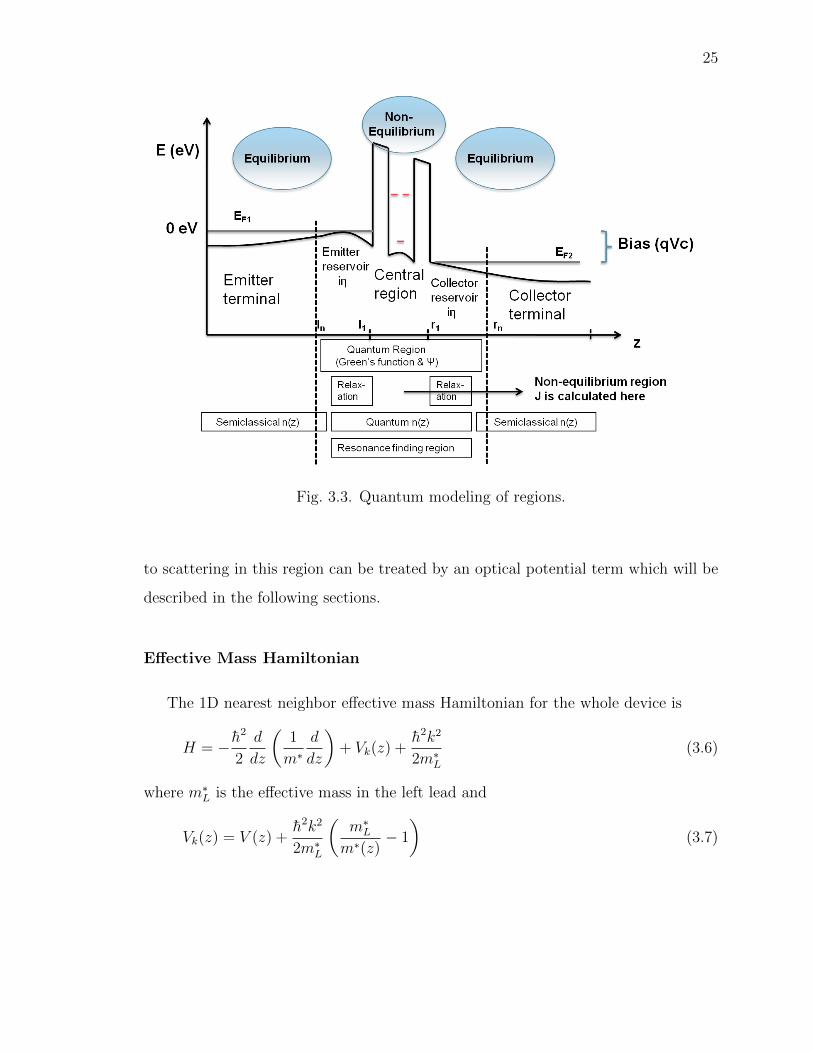
3.2.2 Hartree Model (Quantum Mechanical treatment)
The device is partitioned into a central region consisting of the two barriers and
the well and reservoirs that inject electrons and draw them out from the central
region. The portion of emitter and collector where flat band conditions exist will be
referred to as terminals while the region between the terminals and the central region,
that includes the spacer, will be referred to as reservoirs. The emitter terminals and
reservoirs are assumed to be in strong equilibrium with an occupation factor f1(E −
EF1) and the collector terminal and reservoir is also assumed to be in equilibrium
but with an occupation factor f2(E−EF2). The central region is in non-equilibrium.
Fig.3.3 demonstrates how the RTD is sectioned
Green’s functions will be computed for the quantum region consisting of the reser-
voirs and the non-equilibrium region. This region also serves as the range within
which charge will be treated quantum mechanically while in the flat band terminal
regions, the charge will be obtained from the semiclassical expression. This reduces
computational burden since the terminals can be very large and including them will
only increase the complexity of the problem.
At high biases, the band bending resulting from the non-uniform doping profile
within the structure gives rise to a triangular potential energy well near the emit-
ter/barrier interface. Quasi bound states are formed in this emitter well and injection
from these quasi bound states must also be considered. The electron sheet density in
this region can be very high and therefore considerable electron-electron and electron-
phonon scattering can be expected here. As a first approximation, the relaxation due
25
Fig. 3.3. Quantum modeling of regions.
to scattering in this region can be treated by an optical potential term which will be
described in the following sections.
Effective Mass Hamiltonian
The 1D nearest neighbor effective mass Hamiltonian for the whole device is
H = − h2
2
d
dz
(1
m∗d
dz
)+ Vk(z) +
h2k2
2m∗L(3.6)
where m∗L is the effective mass in the left lead and
Vk(z) = V (z) +h2k2
2m∗L
(m∗Lm∗(z)
− 1
)(3.7)

26
The H matrix is obtained by discretizing the above operator and is of the form
• •
• • •
−t1,0 ε1 −t1,2−t2,1 ε2 −t2,3
−t3,2 ε3 −t3,3• • •
• •
(3.8)
where
εi =h2
∆2
(1
m∗i−1 +m∗i+
1
m∗i +m∗i+1
)+ Vi(k) (3.9)
ti,j =h2
∆2
1
m∗i +m∗j(3.10)
As the discretization is done in real space, the matrix elements are scalar quan-
tities. However, if orbital basis functions are used then each of the matrix elements
would be a sub-matrix of size equal to the number of orbital basis functions used.
Open boundary conditions have to be applied to Eq.(3.8) to account for charge
flow into and out of the non-equilibrium region.
Non-Equlibrium Green’s Function method
NEGF is a convenient approach for treating open systems and their interaction
with contacts. An exact treatment of semi-infinite contacts is possible.
In the sections that follow, the notations used in [15] will be adopted. The deriva-
tion follows the approach in [16].
The Green’s function for the whole device in the absence of scattering is
G = [EI −H]−1 (3.11)
Let
A′ = [EI −H] (3.12)
27
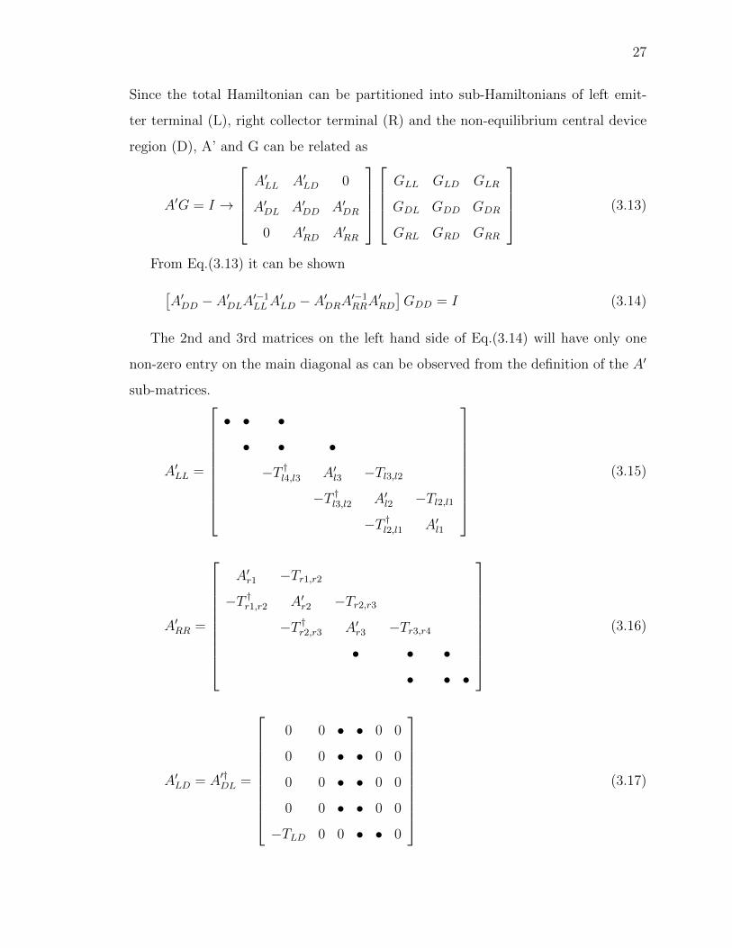
Since the total Hamiltonian can be partitioned into sub-Hamiltonians of left emit-
ter terminal (L), right collector terminal (R) and the non-equilibrium central device
region (D), A’ and G can be related as
A′G = I →
A′LL A′LD 0
A′DL A′DD A′DR
0 A′RD A′RR
GLL GLD GLR
GDL GDD GDR
GRL GRD GRR
(3.13)
From Eq.(3.13) it can be shown[A′DD − A′DLA′−1
LLA′LD − A′DRA′−1
RRA′RD
]GDD = I (3.14)
The 2nd and 3rd matrices on the left hand side of Eq.(3.14) will have only one
non-zero entry on the main diagonal as can be observed from the definition of the A′
sub-matrices.
A′LL =
• • •
• • •
−T †l4,l3 A′l3 −Tl3,l2−T †l3,l2 A′l2 −Tl2,l1
−T †l2,l1 A′l1
(3.15)
A′RR =
A′r1 −Tr1,r2−T †r1,r2 A′r2 −Tr2,r3
−T †r2,r3 A′r3 −Tr3,r4• • •
• • •
(3.16)
A′LD = A′†DL =
0 0 • • 0 0
0 0 • • 0 0
0 0 • • 0 0
0 0 • • 0 0
−TLD 0 0 • • 0
(3.17)

28
A′RD = A′†DR =
0 0 • • 0 −T ′RD0 0 • • 0 0
0 0 • • 0 0
0 0 • • 0 0
0 0 0 • • 0
(3.18)
Next the Green’s function for the isolated semi-infinite terminals is defined as
gL = A′−1LL and gR = A′−1
RR (3.19)
The surface Green’s function for the left and right terminals are Green’s function
elements corresponding to the edge layers l1 and r1 respectively.
gLl1,l1 = (A′−1LL )1,1 and gRr1,r1 = (A′−1
RR)1,1 (3.20)
Eq.(3.14) can be written using Eq.(3.20) as
[A′DD − ΣL − ΣR]GDD = I (3.21)
[EI −HDD − ΣL − ΣR]GDD = I (3.22)
where
ΣL = TDLgLl1,l1TLD (3.23)
ΣR = TDRgRr1,r1TRD (3.24)
are the self-energies for left and right terminals respectively.
Green’s function and Correlation function
The definition of Green’s function for the central non-equilibrium plus the equi-
librium reservoir region (D) follows from Eq.(3.22).
G′ = [EI −HDD − ΣL − ΣR]−1 (3.25)

29
Fig. 3.4. Computation of left connected Green’s function and fullyconnected Green’s function.
where the effect of the terminals has been folded into region D using ΣL and ΣR.
The submatrix of G′ corresponding to the non-equilibrium region alone would be
G = [EI −Hd − Σ1 − Σ2]−1 (3.26)
where Hd is the submatrix of Hamiltonian H corresponding to the non-equilibrium
region and Σ1 and Σ2 are the self-energies that take into account the coupling to the
left and right equilibrium reservoirs. Σ1 and Σ2 are related to the surface Green’s
function at layers l1 and r1 respectively.
Σ1 = Tl1,1gLl1,l1T1,l1 (3.27)
Σ2 = TN,r1gRr1,r1Tr1,N (3.28)

30
The in-scattering self-energies due to equilibrium reservoirs Σ1 and Σ2 are defined
as
Σin1 (E) = −2Im[Σ1(E)]f1(E) = Γ1(E)f1(E) (3.29)
Σin2 (E) = −2Im[Σ2(E)]f1(E) = Γ2(E)f2(E) (3.30)
where Γ1 and Γ2 are the broadening functions. The electron correlation function Gn
for the non-equilibrium region is given by
Gn = G(Σin1 + Σin
2 )G† (3.31)
In the next section a technique to quickly generate the necessary elements of G′
(of which G is a submatrix) and Gn will be presented.
Recursive Green’s function method
In order to determine the elements of G′, Eq.(3.24) and Eq.(3.25) show that gLl1,l1
and qRr1,r1 need to be computed first.
In the following derivation, only the left terminal will be treated. The right
terminal can be treated in a similar fashion. To determine gLl1,l1, the following
equation needs to be solved recursively.[A′l − T
†l gLl1,l1Tl
]gLl1,l1 = I (3.32)
Once we have gLl1,l1 the elements down the main diagonal of the left-connected
Green’s functions can be determined successively from Dyson’s equation
gLq+1q+1,q+1 =
(Aq+1,q+1 − Aq+1,qg
Lqq,qAq,q+1
)−1(3.33)
where the site index q+1 varies from ln to N. For indices ln to l1, an energy dependent
optical potential term iη is added to the diagonal elements of H appearing in A. The
energy dependence can be chosen to be either exponential or Lorentzian or a constant
value. This imaginary term determines the scattering induced broadening in the

31
equilibrium reservoir region just as the imaginary part of the self-energy (Eq.(3.30))
determines the intrinsic broadening due to coupling to the reservoirs. Because of η,
the density of states around the emitter quasi-bound state in the equilibrium reservoir
is broadened and takes the form
D(E) =η(E)/2π
(E − ε)2 + η(E)2(3.34)
When the index q + 1 reaches l1, the self-energy terms Σ1 and Σ2 defined in
Eq.(3.28) can be constructed.
The last element obtained from above step, gLNN,N is same as the last diagonal
element of the fully connected Green’s function, GN,N (or G′N,N) for the quantum
region.
Starting from the last element GN,N the other elements of G can be determined
successively using
Gq+1,q = −Gq+1,q+1Aq+1,qgLqq,q (3.35)
Gq,q+1 = −gLqq,qAq,q+1Gq+1,q+1 (3.36)
Gq,q = gLqq,q − gLqq,qAq,q+1Gq+1,q (3.37)
For the equilibrium reservoir region, Eq.(3.37) can be used to get the diagonal
elements of G′ which are the only ones needed for computing quantum charge in the
equilibrium region.
The correlation function for the non-equilibrium region can be obtained from G
through
Gn = G (Γ1f1 + Γ2f2)G† (3.38)
The above equation shows that only the 1st and Nth column of G are required to
compute Gn.
Similarly, for the equilibrium reservoir region, the diagonal elements of the corre-
lation function are
Gnq,q = if1
(G′q,q −G′†q,q
)(3.39)

32
Charge density
The electron density in the quantum region is obtained through
nq(E) = 2Gnq,q(E)
2π(3.40)
nq = 2
∫dE
2πGnq,q(E) (3.41)
3.3 Transport
For both Thomas-Fermi and Hartree models, transmission and current are calcu-
lated by using the NEGF formalism. The difference lies in the kind of self-consistent
potential that is passed on to the NEGF solver.
• In Thomas-Fermi method, the electrostatic potential is solved self-consistently
with semiclassical charge and then finally passed to the NEGF solver for deter-
mining the tranmission and current.
• In Hartree method, the electrostatic potential that is passed to the NEGF solver
is calculated self-consistently with the quantum charge obtained from a previous
NEGF calculation. Once the quantum charge and potential have converged,
the transmission and current from the last NEGF calculation are treated as the
result.
3.3.1 Transmission and Current
Both transmission and current are computed only within the non-equilibrium
region. The transmission at energy E is
T (E) = Tr[Γ1(E)G(E)Γ2(E)G†(E)
](3.42)

33
The above equation shows that the off-diagonal (1, N) element ofG is the only element
that is needed. An efficient technique to compute T(E) that uses only the (1, 1)
element is
A = GΓ1G† +GΓ2G
† (3.43)
T (E) = Tr{
Γ1
[A−GΓ1G
†]} (3.44)
In the phase coherent limit, the current can be calculated using
I =2e
h
∫dE
2πT (E) [f1(E)− f2(E)] (3.45)
The energy grid used for numerically evaluating the integrals in Eq.(3.41) and
Eq.(3.45) are determined based on the resonance levels found by the resonance finder.
Since the transmission probability is peaked at energies around the resonance level,
the contribution to the integrals will be more at these energies. So a finer grid would
be required to resolve the contribution at these energies.
Once the quantum charge density for the non-equilibrium and the equilibrium
reservoir region is obtained, it is concatenated with the semiclassical density obtained
for the flat band region in the terminals. From this charge profile, a quasi Fermi level
is extracted and a semiclassical density-Poisson self-consistent calculation is carried
out.
3.4 Self-consistent electrostatic potential calculation
The Poisson equation
d
dz
(ε(z)
dΦ
dz
)= q
(n(z)−N+
D
)(3.46)
is discretized to get
Fi =1
a2
(Φi−1ε
− − Φi(ε− + ε+) + Φi+1ε
+)
+ q(ND
+i − ni
)= 0 (3.47)
where
ε+ =εi + εi+1
2(3.48)
ε− =εi + εi−1
2(3.49)

34
Fig. 3.5. Simulation flow for Hartree self-consistent simulation for onebias voltage value.
Eq.(3.47) can be solved for Φ using Newton-Raphson iteration technique∑j
∂Fmi
∂Φmj
δΦm+1j = −Fm
i (3.50)
where
Φm+1 = Φm + δΦm+1 (3.51)
Eq.(3.50) requires ni and ∂ni/∂Φj
ni = NcF1/2
(EF i − Eci + qΦi
kBT
)(3.52)
∂ni∂Φj
= δi,jq
kBTNcF−1/2
(EF i − Eci + qΦi
kBT
)(3.53)

35
For Hartree method, using the quantum mechanical charge, Eq.(3.52) can be
inverted to obtain a quasi-Fermi level which is then used in the Jacobian calculation
step (Eq.(3.53).
3.5 Thomas-Fermi vs Hartree method
The potential profiles and current-voltage characteristics obtained from Thomas-
Fermi calculation and from Hartree self-consistent calculation differ mainly due to the
well charge that is taken into account in the case of Hartree self-consistent method.
The structure described in Table 3.1 will be used for the following discussion.
Layer Material Length Doping
(nm) (/cm3)
Lead1 GaAs 30 1× 10¹⁸
Spacer1 GaAs 10 1× 10¹⁵
Barrier1 AlGaAs 5 1× 10¹⁵
Well1 GaAs 5 1× 10¹⁵
Barrier2 AlGaAs 5 1× 10¹⁵
Spacer2 GaAs 10 1× 10¹⁵
Lead2 GaAs 30 1× 10¹⁸
Table 3.1GaAs/AlGaAs DBRTD structure used in the simulations.
3.5.1 Conduction band profile
The conduction band profile under non-equilibrium conditions is obtained by
adding the selfconsistent potential energy to the equilibrium conduction band profile.
Fig.3.6 shows the conductions band profile at 0.175 V obtained from a Thomas-Fermi
semiclassical and Hartree quantum self-consistent calculation. There is not much de-

36
Parameter Value
Temperature 300 K
Mesh size 0.2833nm
Cross-sectional area 100nm× 100nm
m∗GaAs 0.067mo
m∗AlGaAs 0.0919mo
εrGaAs 13.18
εrAlGaAs 12.0105
ECGaAs 1.424 eV
ECAlGaAs 1.7019 eV
Table 3.2Simulation parameters for GaAs/AlGaAs DBRTD structure used inthe simulations.
viation except that in the well region the Hartree method shows that the conduction
band and resonances have been raised in energy over the Thomas-Fermi result. This
is due to the influence of the electrons tunneling into the well.
3.5.2 Free charge density
A comparison of free charge density obtained from the 2 techniques is shown
in Fig.3.7. The blue curve labelled Thomas-Fermi + Hartree(1 pass) is obtained by
using the slef-consistent electrostatic potential obtained at the end of the Thomas-
Fermi semiclassical calculation in the NEGF quantum charge equation.
The semiclassical free charge density (in black) is zero in the barriers and quantum
well and it shows a trend of accumulation near the emitter/barrier interface and
depletion near the collector/barrier interface.

37
Fig. 3.6. Conduction band edge profile obtained from semiclassi-cal Thomas Fermi model (blue) and Hartree quantum self-consistentmethod (red). The upward shift for the Hartree result in the wellregion is due to the presence of charge in the well which pulls theconduction band edge and the resonance level upwards in energy asagainst the applied bias which tries to pull them down

38
The quantum charge (in red) in the center of the quantum well increases with
bias till the peak voltage is reached and then for higher biases it drops as the second
barrier’s effective height reduces.

39
Fig. 3.7. Comparison of electron density obtained from a Thomas-Fermi and Hartree quantum self-consistent caclculations for differentbias voltages applied to the DBRTD. The 2nd plot is at peak voltageVc = 0.2V

40
Fig. 3.8. IV characteristics computed from semiclassical ThomasFermi model (blue) and Hartree quantum self-consistent method (red)
3.5.3 Current
A comparison of the IV characteristics for the Thomas-Fermi and Hartree quantum
self-consistent techniques is shown in Fig. 3.8.
The Hartree model predicts a larger peak current and peak voltage. The reason
for this can be deduced from the conduction band edge profile for an intermediate
voltage point as shown in Fig. 3.6
A larger voltage is needed in the Hartree case to pull down the conduction band
and resonance level within the well, therefore, resulting in a larger peak voltage over
the semiclassically predicted one.

41
Fig. 3.9. Variation of first 2 resonances (in red) for Thomas-Fermi(left) and Hartree quantum self-consistent (right) methods. Theemitter Fermi level (in blue), the conduction band edge at the leftspacer/barrier interface (bottom black line) and the peak conductionband edge to the left of the barrier (top black line) are also shown.
This same observation can also be made from the resonance vs voltage plots
obtained from the two methods.
The bump in the resonance vs. voltage plot for the Hartree self-consistent method
is due to the charge in the well that is trying to pull the resonance up in energy.
Beyond the peak voltage, the resonance starts dropping rapidly with applied bias
similar to the case of Thomas-Fermi calculation. This is due to reduction in the
effective height of the second barrier as the bias is increased (Fig.3.10). The 2nd
barrier becomes more and more transparent and hence the well charge moves into the
collector side.

42
Fig. 3.10. Conduction band edge profile (top), quantum charge den-sity (center, blue) at 0.475 V and variation of quantum charge (bot-tom, orange), semiclassical charge (bottom, red) with bias in the non-equilibrium device region. As the 2nd barrier becomes shorter withbias, the well charge diminishes.

43
Fig. 3.11. Conduction band profile (left),transmission coefficient (cen-ter,blue), current density (center, dark green), normalized cumulativecurrent density (center, light green) and resonance energy vs voltageat peak voltage of 0.2V. The normalized cumulative current densityshows that the 1st resonance level is the major contributor to thetotal current.
3.6 Cumulative current density
The cumulative current density plot gives information about each resonance level’s
contribution to the total current that flows for a particular applied voltage. At peak
voltage, it can be seen from Fig.3.11 that nearly 92% of the total current is carried by
the 1st resonance. As the bias increases, the 1st resonance drops below the emitter
conduction band and ceases to contribute to current flow (Fig.3.12). The current that
flows then is entirely due to higher order resonances.
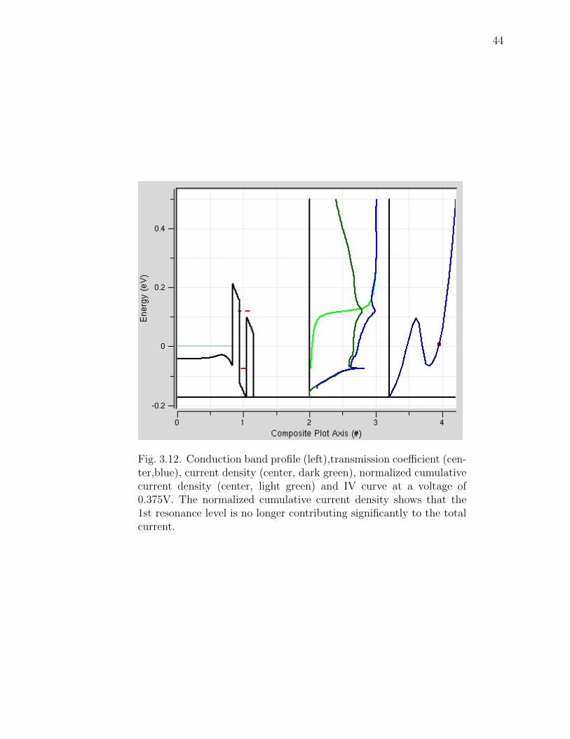
44
Fig. 3.12. Conduction band profile (left),transmission coefficient (cen-ter,blue), current density (center, dark green), normalized cumulativecurrent density (center, light green) and IV curve at a voltage of0.375V. The normalized cumulative current density shows that the1st resonance level is no longer contributing significantly to the totalcurrent.

45
3.7 2D-2D Tunneling
For high biases, as explained before, the band bending in emitter region close to
the barrier results in a triangular potential well. The narrow subbands that result
in this emitter notch can act as sources of electrons for the tunneling process. The
tunneling between these emitter quasi-bound states and the well quasi-bound states
is referred to as 2D-2D tunneling in contrast with the 3D-2D tunneling between the
bulk emitter states and the well subbands.
Fig. 3.13. Emitter quasi-bound state (left, orange) at an applied biasof 0.68V. Tunneling from this quasi-bound state into well resonancecontributes some current although its magnitude is much smaller thanthe current arising from the higher order well resonance.

46
Electrons from the emitter terminal are injected into the quasi-bound states in the
emitter by scattering processes resulting in some broadening which has been mimicked
by adding an imaginary potential term (iη) to the on-site Hamiltonian elements for
the emitter notch region. By including the emitter spacer region close to the barrier
in the NEGF equations, the quasi-bound states resulting from confinement within
the emitter notch can be accounted for automatically.
3.8 Summary
In this chapter, the modeling techniques used in the NEMO5 based RTD NEGF
simulation tool were discussed. The energy band diagrams resulting from a self-
consistent semiclassical Thomas-Fermi and Hartree quantum charge methods were
presented and it was seen that they were nearly identical but for the contribution of
the well charge in the Hartree method.
47
4. RESONANT INTERBAND TUNNELING DIODES
4.1 Introduction
The low PVR of RTDs has necessiated research into techniques to reduce the valley
current. Resonant interband tunneling diodes which combine the resonant transmis-
sion phenomenon through undoped layers of RTDs and the band-to-band tunneling
behaviour of Esaki diodes have been shown to offer good PVRs. An overview of Esaki
diode is presented first followed by the operation of an InAs/AlSb/GaSb RITD and
the NEGF simulation results with an sp3s* tight binding model.
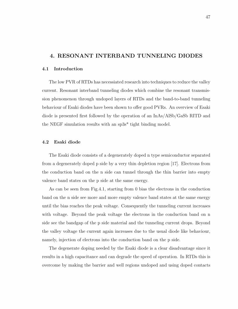
4.2 Esaki diode
The Esaki diode consists of a degenerately doped n type semiconductor separated
from a degenerately doped p side by a very thin depletion region [17]. Electrons from
the conduction band on the n side can tunnel through the thin barrier into empty
valence band states on the p side at the same energy.
As can be seen from Fig.4.1, starting from 0 bias the electrons in the conduction
band on the n side see more and more empty valence band states at the same energy
until the bias reaches the peak voltage. Consequently the tunneling current increases
with voltage. Beyond the peak voltage the electrons in the conduction band on n
side see the bandgap of the p side material and the tunneling current drops. Beyond
the valley voltage the current again increases due to the usual diode like behaviour,
namely, injection of electrons into the conduction band on the p side.
The degenerate doping needed by the Esaki diode is a clear disadvantage since it
results in a high capacitance and can degrade the speed of operation. In RTDs this is
overcome by making the barrier and well regions undoped and using doped contacts
48
Fig. 4.1. Esaki diode operation.

49
to supply the carriers. The PVR of Esaki diodes on the other hand is usually much
better than RTDs.
RITDs combine the desirable features of Esaki diodes and RTDs in that their
PVR is good like Esaki diodes and like RTDs the barrier and well are undoped
resulting in a low capacitance and hence high switching speed as well as being easier
to fabricate [18], [19], [20].
4.3 InAs/AlSb/GaSb RITD
The conduction band profile of a typical RITD with AlSb barriers, GaSb quantum
well and InAs contact layers is shown in Fig.4.2.
Fig. 4.2. Equilibrium band diagram for an InAs/AlSb/GaSb RITD.
The InAs/AlSb/GaSb system form a Type II heterostructure with the conduction
offsets such that the valence band maximum of GaSb is above the conduction band
minimum of InAs. The electrons from the InAs emitter can tunnel through the AlSb

50
barrier into quantized valence band states in GaSb and then into the collector through
the 2nd AlSb barrier. Since the tunneling process involves conduction band states
in emitter and valence subbands in the well, it is referred to as interband tunneling.
The width of the quantum well is chosen such that a quantized valence band state is
present in the well at an energy above the conduction band edge of the emitter. The
overlap between the well valence subband and the emitter bands for energies below the
emitter Fermi level (assuming 0K) gives the number of electron k states particpating
in the tunneling process. At equilibrium there is an overlap between emitter bands
and the valence subband in the well (Fig.4.3). But because of the Fermi levels in the
emitter and collector being at the same energy, no current flows. When the positive
bias applied to the RITD increases, the valence subband minimum in the well drops.
For a particular value of the applied bias, the well subband minimum falls below the
conduction band edge in the emitter. This is when the current starts to decay. For an
intermediate value of the bias, the current rreaches a peak value. For more positive
biases, the tunneling electrons see the bandgap of GaSb and so the transmission
probability is greatly reduced. This is illustrated in Fig.4.4.
If the bias voltage is increased further, then the electrons from the conduction
band of emitter can tunnel into conduction subbands in the GaSb quantum well for
electrons. This is the regular resonant tunneling phenomenon that was described in
the preceding chapters.
The advantage of RITDs is that in the valley current regime, the electrons have
to tunnel through not only the AlSb barriers but also through the bandgap of GaSb
layer which is relatively thick. Therefore the transmission probability is reduced for
the voltages in the valley regime and this translates into a higher PVR.

51
Fig. 4.3. Equilibrium band diagram and overlap between InAs emit-ter bands and GaSb valence subband dispersions along kx for anInAs/AlSb/GaSb RITD.
Fig. 4.4. Band diagram for voltages greater than peak voltage andoverlap between InAs emitter bands and GaSb valence subband dis-persions along kx for an InAs/AlSb/GaSb RITD.

52
4.4 Multiband modeling
As the operation of RITDs involves both the conduction band and the valence
band, the single band effective mass model described in the previous chapter is
inadequate. Atleast a 2 band model is needed to compute the IV characteristics
[21], [22], [23]. The NEMO5 simulator in conjunction with an sp3s* tight binding
model that takes into account electron spin-orbit coupling has been used to study an
InAs/AlSb/GaSb RITD.
The RITD is treated as a sequence of monolayers that are parallel to the interfaces.
Let M represent the number of orbitals per unit cell in the tight binding basis set
(M = 20 for sp3s* model with spin orbit coupling included). The basis orbitals can
be written as∣∣R||σα⟩, where σ = 1, 2, ...,M is the integer monolayer label, R|| is the
in-plane component of unit cell coordinate and α = 1, 2, ...,M represents the orbitals
within a unit cell.
The wave function can be written as
|Ψ〉 =∑σ,α
Cσα∣∣σα,k||⟩ (4.1)
where∣∣σα,k||⟩ is a planar orbital formed by taking Bloch sums of tight-binding
orbitals over the N|| unit cells in the σth monolayer∣∣σα,k||⟩ =1√N||
∑R||
ejk||.R||∣∣R||σα⟩ (4.2)
The Schrodinger equation (H −E) |Ψ〉 = 0 can be expressed in the planar orbital
basis as
Hσ,σ−1Cσ−1 + Hσ,σCσ + Hσ,σ+1Cσ+1 = 0 (4.3)
where Cσ is a vector of length M ,
Cσ =
Cσ1
Cσ2
...
CσM
(4.4)
53
and Hσ,σ′ and Hσ,σ are M ×M matrices whose elements are given by
(Hσ,σ′)α,α′ =⟨σα,k|| |H|σ′α′,k||
⟩(4.5)
and
(Hσ,σ
)α,α′
=⟨σα,k|| |(H − E)|σα′,k||
⟩(4.6)
where the resultantH is the tight binding Hamiltonian whose matrix elements (orbital
on-site energies and overlap elements) are chosen in such a way that they reproduce
the bulk band gaps along the important crystal symmetry directions [24], [25].
Once the Hamiltonian has been expressed in the planar orbital basis, the Green’s
function for the device and self-energies can be derived and the charge density com-
puted in a manner analogous to that described in Chapter 3 for effective mass mod-
eling. The matrix elements in this case would be of size M ×M .
4.5 Current density
The expression for current Eq.(3.45) assumes a parabolic dispersion in the trans-
verse direction. In the case of multiband calculation, the bandstructure along the
transverse direction will appear in the current calculation through the dependence of
transmission probability and occupation factor on k|| [10].
J =2q
(2π2)h
∫ ∫T (E,k||)[fE(E)− fC(E)]dEdk|| (4.7)
4.6 Simulation Results
4.6.1 IV characteristics
The RITD structure simulated using NEMO5 simulator is described in Table 4.1
A Thomas-Fermi semiclassical calculation was performed for this structure and the
IV curve obtained is shown in Fig.4.5 The simulated IV curve shows that the PVR is
50 and the valley current has been reduced considerably compared to the peak current.

54
Layer Material Monolayers Doping
(/cm3)
Lead1 InAs 100 1× 10¹⁸
Spacer1 InAs 16 1× 10¹⁵
Barrier1 AlSb 4 1× 10¹⁵
Well1 GaSb 16 1× 10¹⁵
Barrier2 AlSb 4 1× 10¹⁵
Spacer2 InAs 16 1× 10¹⁵
Lead2 InAs 100 1× 10¹⁸
Table 4.1InAs/AlSb/GaSb RITD structure used in the simulations.
Fig. 4.5. IV curve for the InAs/AlSb/GaSb RITD at 300K showing a PVR of 50.

55
The valley current region is also relatively broad extending from around 0.3V to 0.7V.
The rise in the current beyond the valley region is attributed to resonant tunneling of
InAs emitter valence band electrons through valence subband in GaSb well and into
empty conduction band states in the InAs collector. In this simulation, only ballistic
transport of electrons is treated. When scattering mechanisms are included, the PVR
is expected to be less than the value obtained from this simulation.
4.6.2 At peak and valley voltage
Current density
The current density J(kx, ky) at peak and valley voltage for 3 different radial k
directions of ky = 0,kx = 0 and kx = ky are shown in Figs.4.6,4.7 and 4.8. The
plots corresponding to peak voltage for all 3 directions look similar. This is due to
isotropic nature of the transverse dispersion. Likewise the plots corresponding to
valley voltage are also identical. For peak voltage, majority of the current flow is due
to the overlap of states around the Γ point as pictured in Fig.4.3. At valley voltage,
the overlap between the energy broadened Γ states (Fig.4.4) is the major contributor
to the current.
Cumulative current density
The cumulative current density at peak voltage and valley voltage along kx is
shown in Fig.4.9. For a particular kx, additional overlap of states between the InAs
conduction and GaSb valence subbands occurs at higher energies. This leads to a
step-like increase in the cumulative current density.
Local density of states
Fig.4.10 shows the energies where the current is flowing. This appears as dark
regions in the local density of states plot.

56
Fig. 4.6. Energy integrated current density J(kx, ky) along kx direc-tion at peak voltage (top) and at valley voltage (bottom).

57
Fig. 4.7. Energy integrated current density J(kx, ky) along ky direc-tion at peak voltage (top) and at valley voltage (bottom).

58
Fig. 4.8. Energy integrated current density J(kx, ky) along kx = kydirection at peak voltage (top) and at valley voltage (bottom).

59
Fig. 4.9. Cumulative current density along ky = 0 at peak voltage(top) and at valley voltage (bottom).

60
Fig. 4.10. LDOS profile along with current density plot for ky = 0direction showing the energy at which the current is flowing for peakvoltage (top) and at valley voltage (bottom).
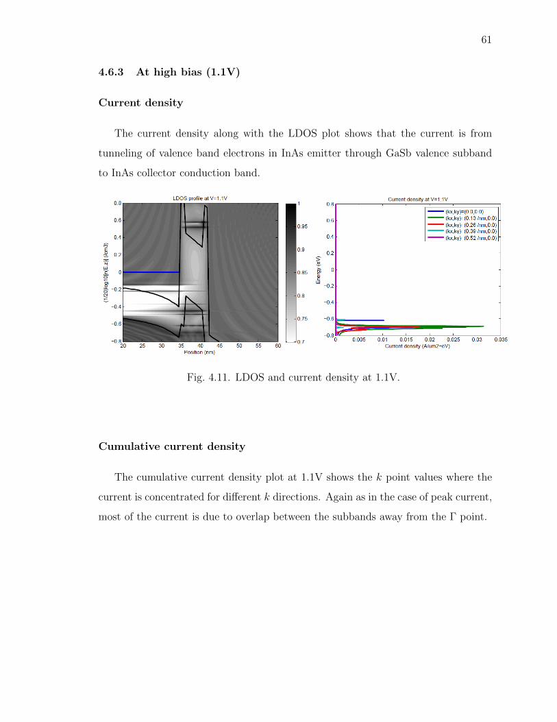
61
4.6.3 At high bias (1.1V)
Current density
The current density along with the LDOS plot shows that the current is from
tunneling of valence band electrons in InAs emitter through GaSb valence subband
to InAs collector conduction band.
Fig. 4.11. LDOS and current density at 1.1V.
Cumulative current density
The cumulative current density plot at 1.1V shows the k point values where the
current is concentrated for different k directions. Again as in the case of peak current,
most of the current is due to overlap between the subbands away from the Γ point.

62
Fig. 4.12. LDOS and current density at 1.1V along kx (top), ky (mid-dle) and kx = ky (bottom).

63
4.7 Applications
Due to their superior PVRs compared to RTDs, InAs/AlSb/GaSb RITDs have
been used to realize logic circuits along with Schottky diodes [26] and also by inte-
grating with HEMTs [27].
4.8 Summary
In this chapter, the operation of InAs/AlSb/GaSb RITDs was described. Due
to the involvement of conduction and valence band a multiband modeling method
is required for RITDs. An sp3s* tight binding model with spin orbit coupling and
NEGF was used to study the characteristics of a coherent RITD. The IV curve for
the considered RITD structure does show a high PVR of the order of 50.

64
5. 1DHETERO AND BRILLOUIN ZONE VIEWER
5.1 1dhetero tool
The 1dhetero tool is a NEMO5 based atomistic simulation tool for studying the
electrostatic properties of 1 dimensional heterostructures [28]. It can be used for
studying the equilibrium properties of channels in HEMTs built using different semi-
conductor materials. The substrate materials that are supported are listed in Table
5.1.
Substrate Materials supported
GaAs GaAs
AlGaAs
AlAs
GaP GaP
AlP
GaSb GaSb
AlSb
InP InP
In53GaAs
In52AlAs
Si Si
Ge
SiO2
Table 5.1Substrates and materials supported by 1dheterostructure tool

65
The tool solves the coupled 1D Schrodinger and Poisson equations self-consistently
along the growth direction for each value of gate voltage. The source and drain
are assumed to be in equilibrium. Hardwall boundary conditions are used for the
Schrodinger equation. For Poisson equation a Dirichlet boundary condition is used
for the gate side and for the bulk side.
Φ(z = 0) = VG (5.1)
Φz = L = 0 (5.2)
The domain for Poisson equation includes the substrate while for computing wave-
functions using Schrodinger equation it is excluded meaning it is assumed that the
wavefunctions decay to 0 along the position axis before reaching the substrate region.
Three types of Hamiltonian models are available -
1. Single band model
2. Tight binding sp3s* model with spin orbit coupling
3. Tight binding sp3d5s* model with sping orbit coupling
Apart from this there is also a semiclassical option that performs a selfconsistent
Thomas-Fermi semiclassical density-Poisson calculation. Since no wave function for-
malism is employed for this option, no Schrodinger equation is solved and hence no
resonances and wave functions will be displayed for this option. The advantage of this
semiclassical approach is that it is very fast even though the electrostatic potential
profile and the free charge density obtained may not be physically correct (Fig.5.5).
Free charge density
The free charge density can be computed using two different techniques
1. The analytical expression for the free charge density is
n(z) =m∗kBT
πh2
∑i
|Ψi(z)|2ln[1 + e
EF−EikBT
](5.3)

66
where Ei is the subband minimum energy. The above equation assumes the
subband dispersion is parabolic in the transverse k plane as is the norm for
effective mass simulation.
2. The numerical k-space summation that considers the exact dispersion in
the transverse k plane, E(kx, ky) is a more rigorous way to account for non-
parabolicity.
n(z) = 2∑i
∑kx,ky
|Ψi(z)|2fo(Ei + E(kx, ky)− EF ) (5.4)
where Ei + E(kx, ky) is the exact dispersion for the subband. The kx, ky grid
for the summation can be set by the user. This technique is used for the tight
binding options.
Outputs
Visualization of the following output results is possible -
1. Conduction/Valence band profile, Fermi level and inversion layer resonances
2. Electrostatic potential
3. Sheet density
4. Resonance energy vs gate voltage
5. Wavefunctions
6. Charge density
7. Doping density

67
Fig. 5.1. Design section of the 1dhetero tool where the dimensionsand doping density of the materials and substrate constituing theheterostructure can be specified.

68
Fig. 5.2. Equilibrium conduction band profile and bound state reso-nances for the default AlGaAs/GaAs heterostructure calculated froma single band simulation.
Fig. 5.3. Equilibrium potential profile for the default AlGaAs/GaAsheterostructure calculated from a single band simulation. The poten-tial peak is due to depletion of carriers in the doped AlGaAs barrier.

69
Fig. 5.4. Equilibrium sheet density profile for the default Al-GaAs/GaAs heterostructure calculated from a single band simulation.A 2DEG is formed near the AlGaAs-GaAs interface resulting in a veryhigh sheet concentration of 8.8× 10¹²/cm2.
Fig. 5.5. Equilibrium sheet density profile for the default Al-GaAs/GaAs heterostructure calculated from a semiclassical Thomas-Fermi simulation. The semiclassical method predicts maximum sheetdensity at the AlGaAs-GaAs interface whereas the single band cal-culation result of Fig.5.4 shows maximum sheet concentration at thecenter of the inversion layer, away from the AlGaAs-GaAs interface.

70
5.2 Brillouin Zone Viewer tool
This is a visualization tool that computes and displays the first Brillouin zone for
various crystal lattice systems [29]. The Brillouin zone is the primitive or Wigner-
Seitz cell of the reciprocal lattice. It includes all the k-points that are closer to a
reciprocal lattice point than its neighbours. The Bloch wavefunctions and the energy
band for periodic crystals can be completely characterized by their behaviour within
a Brillouin zone.
The lattice systems available are-
1. Cubic systems - Simple cubic, FCC, BCC
2. Wurtzite - Hexagonal
3. Honeycomb - Graphene
4. Rhombohedral
The inputs to the tool are the lattice translational vectors which don’t necessarily
have to be that of the conventional unit cell. For cubic crystal systems, the lattice
vectors can be specified either in terms of the standard orthogonal co-ordinate sys-
tem basis or in the basis of the primitive translational vectors. For example, the
translational vectors for FCC lattice are
−→a1 =a0
2(−→ax +−→ay) (5.5)
−→a2 =a0
2(−→ay +−→az) (5.6)
−→a3 =a0
2(−→ax +−→az) (5.7)
where a0 is the lattice constant. In the standard xyz orthogonal co-ordinate sys-
tem basis, the above translational vectors can be specified using the components of
−→ax,−→ay ,−→az , i.e., as (110),(011) and (101) respectively.
In the basis of the primitive vectors, the same vectors can be specified as com-
ponents of −→a1 ,−→a2 ,−→a3 , i.e., as (100),(010) and (001) respectively. This is the default
specification option for non-cubic systems used in the tool.

71
Fig. 5.6. Brillouin zone viewer tool showing the 1st Brillouin zone forthe cubic FCC lattice.

72
6. SUMMARY
In this thesis, the NEMO5 based RTD NEGF simulation tool was presented for
GaAs/AlGaAs RTDs. The procedure used and results obtained from a coherent
simulation of 1D transport in GaAs/AlGaAs RTDs using effective mass model and
NEGF were demonstrated. The effect of scattering in the emitter reservoir region has
been treated by including an optical potential term in the self-energy calculation. This
technique eases the computational burden that would otherwise have to be tolerated if
scattering were treated in a rigorous fashion. For improved results and a closer match
to experimental IV, a realistic treatment of electron-phonon interaction throughout
the device via self-energies would be necessary.
Future work for this tool would be the addition of tight binding option to account
for atomistic effects. Material system apart from GaAs/AlGaAs such as GaAs/AlAs,
InGaAs/InAlAs, etc. could be a useful addition to the tool. The wafer orientation
for the RTDs, which has been set to (100) here, could be included as an option.
(111) oriented GaAs/AlAs RTDs have been reported with PVRs larger than (100)
counterparts [30]. A simulation tool capabling of handling different wafer orientations
of RTDs would be a valuable aid.
Apart from effective mass simulation of RTDs, an sp3s* tight binding model was
used to simulate an InAs/AlSb/GaSb coherent RITD. The PVR for RITDs tend to
be higher due to the reduction in the valley current by introduction of the GaSb layer.
A simulation tool similar to RTD NEGF can be developed exclusively for studying
the characteristics of InAs/AlSb/GaSb RITDs.
Two other simulation tools - 1dheterostructure and Brillouin zone viewer powered
using NEMO5 were also developed during the course of this work and the modeling
techniques used were described in the concluding chapter. The 1dheterostructure tool
can be used for simulation of heterostructures such as HEMT structures with only a

73
gate voltage applied and no source to drain voltage. A natural extension to this could
be the addition of source to drain voltage and the option of determining the current
voltage characteristics. An accurate treatment of contacts will have to be included
for this. As for the Brillouin zone viewer, crystal lattice systems apart from cubic,
honeycomb, hexagonal and rhombohedral could be added.

LIST OF REFERENCES

74
LIST OF REFERENCES
[1] L.L. Chang, L. Esaki, and R. Tsu, “Resonant tunneling in semiconductor doublebarriers,” Applied Physics Letters, vol. 24, p. 593, 1974.
[2] T.C.L.G. Sollner, W.D. Goodhue, P.E. Tannenwald, C.D. Parker, and D.D. Peck,“Resonant tunneling through quantum wells at frequencies up to 2.5 THz,” Ap-plied Physics Letters, vol. 43, p. 588, 1983.
[3] Pinaki Mazumder, Shriram Kulkarni, Mayukh Bhattacharya, Jian Ping Sun, andGeorge I. Haddad, “Digital Circuit Applications of Resonant Tunneling Devices,”Proceedings of the IEEE, vol. 86, April 1998.
[4] J.P.A. van der Wagt, A.C. Seabaugh, and E.A. Beam, III, “RTD/HFET LowStandby Power SRAM Gain Cell,” IEEE Electron Device Letters, vol. 19, Jan-uary 1998.
[5] B. Prince, Emerging memories: technologies and trends. Kluwer Academic Pub-lishers, 2002.
[6] A. Seabaugh, B. Brar, T. Broekaert, F. Morris, P. van der Wagt, and G. Frazier,“Resonant-tunneling mixed-signal circuit technology,” Solid-State Electronics,vol. 43, pp. 1355–1365, 1999.
[7] B.Ricco and M.Ya.Azbel, “Physics of resonant tunneling. The one-dimensionaldouble-barrier case,” Physical Review B, vol. 29, p. 1970, February 1984.
[8] H. Mizuta and T. Tanoue, The Physics and Applications of Resonant TunellingDiodes. Cambridge University Press, 1995.
[9] Jian Ping Sun, George I. Haddad, Pinaki Mazumder, and Joel N. Schulman,“Resonant Tunneling Diodes: Models and Properties,” Proceedings of the IEEE,vol. 86, p. 641, April 1998.
[10] R.C. Bowen, G. Klimeck, and R.K. Lake, “Quantitative simulation of a resonanttunneling diode,” Journal of Applied Physics, vol. 81, no. 7, 1996.
[11] R. Tsu and L. Esaki, “Tunneling in a finite superlattice,” Applied Physics Letters,vol. 22, pp. 562–564, 1973.
[12] S. Luryi, “Frequency limit of double-barrier resonant-tunneling oscillators,” Ap-plied Physics Letters, vol. 47, p. 490, 1985.
[13] S. Luryi, “Mechanism of operation of double-barrier resonant-tunneling ocsilla-tors,” International Electron Devices Meeting, 1985, pp. 666–669, 1985.
[14] S. Luryi, “Coherent versus incoherent resonant tunneling and implications forfast devices,” Superlattices and Microstructures, vol. 5, p. 375, 1989.

75
[15] S. Datta, Quantum Transport: Atom to Transistor. Cambridge University Press,2005.
[16] M.P. Anantram, Mark S. Lundstrom, and Dmitri E. Nikonov, “Modeling ofNanoscale Devices,” Proceedings of the IEEE, vol. 96, September 2008.
[17] L. Esaki, “New Phenomenon in Narrow Germanium p-n Junctions,” PhysicalReview, vol. 109, p. 603, 1958.
[18] M. Sweeny and J. Xu, “Resonant interband tunnel diode,” Applied Physics Let-ters, vol. 54, p. 546, 1989.
[19] J.R. Soderstrom, D.H. Chow, and T.C. McGill, “A new negative differential re-sistance device based on resonant interband tunneling,” Applied Physics Letters,vol. 55, p. 1094, 1989.
[20] L.F. Luo, R. Beresford, and W.I. Wang, “Interband tunneling in polytypeGaSb/AlSb/InAs heterostrutures,” Applied Physics Letters, vol. 55, p. 2023,1989.
[21] M. Ogawa, T. Sugano, and T. Miyoshi, “Multi-band simulation of quantumtransport in resonant interband tunneling devices,” Physica E: Low-dimensionalSystems and Nanostructures, vol. 7, p. 840, 2000.
[22] M. Ogawa, T. Sugano, and T. Miyoshi, “Tight binding simulation of quantumelectron transport in type II resonant tunneling devices,” Extended Abstracts of1998 Sixth International Workshop on Computational Electronics, p. 152, 1998.
[23] Roger Lake, Gerhard Klimeck, R. Chris Bowen, and Dejan Jovanovic, “Singleand multiband modeling of quantum electron transport through layered semi-conductor devices,” Journal of Applied Physics, vol. 15, June 1997.
[24] G. Klimeck, R.C. Bowen, T. Boykin, and T.A. Cwik, “sp3s* Tight-Binding Pa-rameters for Transport Simulations in Compound Semiconductors,” Superlatticesand Microstructures, vol. 27, no. 5-6, pp. 519–524, 2000.
[25] P. Vogl, H. P. Hjalmarson, J. D. Dow, and T.A. Cwik, “sp3s* Tight-BindingParameters for Transport Simulations in Compound Semiconductors,” J. Phys.Chem. Solids, vol. 44, no. 5, pp. 365–378, 1983.
[26] D.H. Chow, H. L. Dunlap, W. Williamson, S. Enquist, B. K. Gilbert, S. Subra-maniam, P.M. Lei, and G. H. Bernstein, “InAs/AISb/GaSb Resonant InterbandTunneling Diodes and Au-on-InAs/A1Sb-Superlattice Schottky Diodes for LogicCircuits,” Electron Device Letters, vol. 17, Febuary 1996.
[27] B.R. Bennett, A.S. Bracker, R. Magno, J.B. Boos, R. Bass, and D. Park, “Mono-lithic integration of resonant interband tunneling diodes and high electron mo-bility transistors in the InAs/GaSb/AlSb material system,” JVST B - Micro-electronics and Nanometer Structures, vol. 18, no. 3, 2000.
[28] 1D Heterostructure Tool, 2011. https://nanohub.org/tools/1dhetero.
[29] Brillouin Zone Viewer, 2011. https://nanohub.org/tools/brillouin.
[30] L.F. Luo, R. Beresford, W.I. Wang, and E.E. Mendez, “Inelastic tunnelingin (111) oriented AlAs/GaAs/AlAs double-barrier heterostructures,” AppliedPhysics Letters, vol. 54, no. 21, 1989.

APPENDIX

76
A. RTD NEGF - USER OPTIONS
The GUI of RTD NEGF simulation tool was developed using the Rappture program-
ming framework. The user options available on the tool will be described in the
following sections.
A.1 Basic options
1. Ambient Temperature - Temperature value that will be used for the Fermi
functions. Default options include 300K (room temperature) and 77K (liquid
Nitrogen boiling point).
2. Starting Bias - Bias voltage at which the emitter terminal will be held fixed.
3. Ending Bias - The collector terminal voltage will be ramped up from the
starting bias voltage value to this value.
4. No. of Points - Determines the bias voltage steps.
5. Potential Model - Thomas-Fermi or Hartree.
6. Quantum Charge - On/off option that is enabled only for Thomas- Fermi
simulation. If this option is set to be OFF then only semiclassical Thomas-
Fermi charge will be displayed. If set to be ON then quantum charge resulting
from NEGF transport calculation will also be displayed.
7. Lattice Constant - Determines real space grid size. Normally half the lattice
constant of the unit cell. In other words thickness of one monolayer of the
substrate.

77
Fig. A.1. RTD NEGF simulation tool showing Basic tab options.

78
Fig. A.2. Multiscale Domains tab options.
A.2 Multiscale Domains options
1. Semiclassical Charge Region - Region where charge is treated semiclassically.
This is used for calculating charge for Hartree model and also for transport
calculation for both Thomas-Fermi and Hartree models. Usually the region
defined as terminal with flat band conditions and in equilibrium.
2. Equilibrium Region - The dimension of the equilibrium reservoir region.
A.3 Advanced options
1. Not-normalized Current Plot - Switching this option to OFF will show the
normalized current density plot.
2. Resonances Scatter Plot - The resonance vs voltage plot will appear as a
scatter plot.
3. Carrier Distribution Surface Plots - Turning this option ON will display
the energy resolved electron density profile.
4. Reservoir Relaxation Model - Option to choose the energy dependence of
η used to account for scattering in the equilibrium reservoir. η can be made to

79
Fig. A.3. Advanced tab options.
reduce exponentially with energy below the emitter quasi-bound state or in a
Lorentzian fashion or in a fixed manner.
5. Reservoir Relaxation Energy - For exponential and Lorentzian roll-off, this
determines the maximum energy value of η.
6. Decay Length - For exponential and Lorentzian roll-off, this determines how
fast with energy η reduces.
7. Use Adaptive Energy Grid - Can be used to control whether an adaptive
energy grid or a fixed energy grid is used for calculation of transmission and
current.
8. Poisson Criterion - Convergence criterion for Poisson-NEGF charge self-consistent
computation (Hartree) or Poisson-semiclassical charge self-consistent computa-
tion (Thomas-Fermi and inner loop of Hartree).

80
Fig. A.4. Resonance Finder tab options.
A.4 Resonance Finder options
1. Resonance Finder - Option to turn ON/OFF display of resonances and wave-
functions.
2. No. of homogeneous grid points - Number of energy grid points used by
resonance finder
3. No. of points per resonance
4. No. of points for Ec EF
5. Lanczos iteration step size - Option for algorithm used to roughly estimate
the location of resonances along energy axis.
6. Lanczos iteration limit - Option for algorithm used to roughly estimate the
location of resonances along energy axis.
7. Newton iteration step size - Option for algorithm used to narrow down the
energy location of the estimated resonance.
8. Newton solver convergence condition - Option for algorithm used to narrow
down the energy location of the estimated resonance.
9. Left exclusion region - Region to the left of the 1st barrier that will be
excluded from the spatial domain used for determining resonance wavefunctions.

81
10. Right exclusion region - Region to the right of the last barrier that will be
excluded from the spatial domain used for determining resonance wavefunctions.