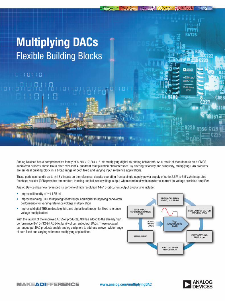
Analog Devices has a comprehensive family of 8-/10-/12-/14-/16-bit multiplying digital-to-analog converters. As a result of manufacture on a CMOS submicron process, these DACs offer excellent 4-quadrant multiplication characteristics. By offering flexibility and simplicity, multiplying DAC products are an ideal building block in a broad range of both fixed and varying input reference applications.
These parts can handle up to ±18 V inputs on the reference, despite operating from a single-supply power supply of up to 2.5 V to 5.5 V. An integrated feedback resistor (RFB) provides temperature tracking and full-scale voltage output when combined with an external current-to-voltage precision amplifier.
Analog Devices has now revamped its portfolio of high resolution 14-/16-bit current output products to include:
• Improved linearity of ±1 LSB INL
• Improved analog THD, multiplying feedthrough, and higher multiplying bandwidth performance for varying reference voltage multiplication
• Improved digital THD, midscale glitch, and digital feedthrough for fixed reference voltage multiplication
With the launch of the improved AD55xx products, ADI has added to the already high performance 8-/10-/12-bit AD54xx family of current output DACs. These updated current output DAC products enable analog designers to address an even wider range of both fixed and varying reference multiplying applications.
Multiplying DACsFlexible Building Blocks
VREFMULTIPLYING
DACS
DIGITALINPUTCODE
8-BIT TO 16-BITRESOLUTION
12MHz MBW
WIDE INPUTREFERENCE RANGE
±18V
FAST SETTLINGTIME 0.1�s
LOW OUTPUT GLITCHIMPULSE 1nV/s
HIGH ACCURACY16-BIT, ±1LSB INL
www.analog.com/multiplyingDAC
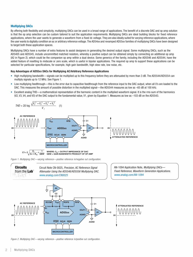
Multiplying DACsBy offering both flexibility and simplicity, multiplying DACs can be used in a broad range of applications. The benefit of a discrete DAC and op amp solution is that the op amp selection can be custom tailored to suit the application requirements. Multiplying DACs are ideal building blocks for fixed reference applications, where the user wants to generate a waveform from a fixed dc voltage. They are also ideally suited for varying reference applications, where the user wants to digitally condition an ac or arbitrary reference voltage. The AD54xx and revamped AD55xx families of multiplying DACs have been designed to target both these application spaces.
Multiplying DACs have a number of extra features to assist designers in generating the desired output signal. Some multiplying DACs, such as the AD5405 and AD5545, include uncommitted matched resistors, whereby a positive output can be obtained simply by connecting an additional op amp (A2 in Figure 2), which could be the companion op amp within a dual device. Some generics of the family, including the AD5546 and AD5544, have the added feature of resetting to midscale or zero scale, which is useful in bipolar applications. The required op amp to support these applications can be selected for particular specifications, for example, high gain bandwidth, high slew rate, low noise, etc.
Key Advantages of AD55xx DACs for Multiplying AC/Arbitrary Reference Applications
• High multiplying bandwidth — signals can be multiplied up to this frequency before they are attenuated by more than 3 dB. The AD5544/AD5554 can multiply signals up to 12 MHz. See Figure 1.
• Low multiplying feedthrough — this is the error due to capacitive feedthrough from the reference input to the DAC output, when all 0’s are loaded to the DAC. This measures the amount of possible distortion in the multiplied signal — the AD5544 measures as low as –65 dB at 100 kHz.
• Excellent analog THD — a mathematical representation of the harmonic content in the multiplied waveform signal. It is the rms sum of the harmonics (V2, V3, V4, and V5) of the DAC output to the fundamental value, V1, given by Equation 1. Measures as low as –103 dB on the AD5543.
5432
1V
VVVVTHD
2222
log20+++
=
(1)
RFB
IOUT1
AGND
SCLK SDIN
VREF
SYNC
AD55xx
VDD
AGND
C1
A1
MICROCONTROLLER
AC REFERENCE
ATTENUATED REFERENCE
0V 0V
GBWRFB
C1C0 1
2�2 ×
×= WHERE: CO = OUTPUT IMPEDANCE OF DAC
GBW = GAIN BANDWIDTH PRODUCT OF OP AMP
Figure 1. Multiplying DAC — varying reference — positive reference in/negative out configuration.
*UNCOMMITTED RESISTOR VERSIONS ONLY
RFB
R1
ROFS
IOUT1
AGND
SCLK SDINSYNC
AD55xxVDD
AGND
C1
A1
A2
MICROCONTROLLER
AC REFERENCEATTENUATED REFERENCE
0V 0V
VREFRCOM
C2
Figure 2. Multiplying DAC — varying reference — positive reference in/positive out configuration.
Circuit Note CN-0025, Precision, AC Reference SignalAttenuator Using the AD5546/AD5556 Multiplying DAC.www.analog.com/CN0025
AN-1094 Application Note, Multiplying DACs — Fixed Reference, Waveform Generation Applications.www.analog.com/AN-1094
2 | Multiplying DACs
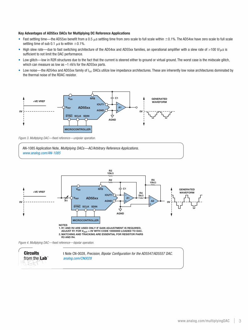
Key Advantages of AD55xx DACs for Multiplying DC Reference Applications
• Fast settling time — the AD55xx benefit from a 0.5 µs settling time from zero scale to full scale within ±0.1%. The AD54xx have zero scale to full scale settling time of sub 0.1 µs to within ±0.1%.
• High slew rate — due to fast switching architecture of the AD54xx and AD55xx families, an operational amplifier with a slew rate of >100 V/µs is sufficient to not limit the DAC performance.
• Low glitch — low in R2R structures due to the fact that the current is steered either to ground or virtual ground. The worst case is the midscale glitch, which can measure as low as –1 nV/s for the AD55xx parts.
• Low noise — the AD54xx and AD55xx family of IOUT DACs utilize low impedance architectures. These are inherently low noise architectures dominated by the thermal noise of the RDAC resistor.
RFB
IOUT1
AGND
SCLK SDIN
VREF
SYNC
AD55xx
VDD
AGND
C1
A1
MICROCONTROLLER
GENERATEDWAVEFORM
0V
+VE VREF
0V
Figure 3. Multiplying DAC — fixed reference — unipolar operation.
AN-1085 Application Note, Multiplying DACs — AC/Arbitrary Reference Applications.www.analog.com/AN-1085
RFB
SCLK SDIN
VREF
SYNC
AD55xx
VDD GENERATEDWAVEFORM
0V
+VE VREF
0V
NOTES1. R1 AND R2 ARE USED ONLY IF GAIN ADJUSTMENT IS REQUIRED. ADJUST R1 FOR VOUT = 0V WITH CODE 10000000 LOADED TO DAC.2. MATCHING AND TRACKING ARE ESSENTIAL FOR RESISTOR PAIRS R3 AND R4.
R1
AGND
C1
A1A2
R2
R310k�
R45k�
R510k�
MICROCONTROLLER
IOUT1
AGND
Figure 4. Multiplying DAC — fixed reference — bipolar operation.
Circuit Note CN-0028, Precision, Bipolar Configuration for the AD5547/AD5557 DAC.www.analog.com/CN0028
www.analog.com/multiplyingDAC | 3
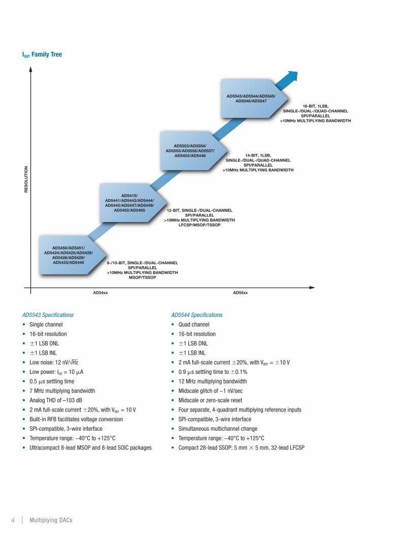
IOUT Family Tree
AD5450/AD5451/AD5424/AD5425/AD5426/
AD5428/AD5429/AD5433/AD5440
AD5415/AD5441/AD5443/AD5444/AD5445/AD5447/AD5449/
AD5452/AD5405
AD5553/AD5554/AD5555/AD5556/AD5557/
AD5453/AD5446
AD5543/AD5544/AD5545/AD5546/AD5547
8-/10-BIT, SINGLE-/DUAL-CHANNEL SPI/PARALLEL
>10MHz MULTIPLYING BANDWIDTH MSOP/TSSOP
12-BIT, SINGLE-/DUAL-CHANNEL SPI/PARALLEL
>10MHz MULTIPLYING BANDWIDTH LFCSP/MSOP/TSSOP
AD54xx AD55xx
RE
SO
LUT
ION
14-BIT, 1LSB,SINGLE-/DUAL-/QUAD-CHANNEL
SPI/PARALLEL>10MHz MULTIPLYING BANDWIDTH
16-BIT, 1LSB,SINGLE-/DUAL-/QUAD-CHANNEL
SPI/PARALLEL>10MHz MULTIPLYING BANDWIDTH
AD5543 Specifications
• Single channel
• 16-bit resolution
• ±1 LSB DNL
• ±1 LSB INL
• Low noise: 12 nV/√Hz
• Low power: IDD = 10 µA
• 0.5 µs settling time
• 7 MHz multiplying bandwidth
• Analog THD of –103 dB
• 2 mA full-scale current ±20%, with VREF = 10 V
• Built-in RFB facilitates voltage conversion
• SPI-compatible, 3-wire interface
• Temperature range: −40°C to +125°C
• Ultracompact 8-lead MSOP and 8-lead SOIC packages
AD5544 Specifications
• Quad channel
• 16-bit resolution
• ±1 LSB DNL
• ±1 LSB INL
• 2 mA full-scale current ±20%, with VREF = ±10 V
• 0.9 µs settling time to ±0.1%
• 12 MHz multiplying bandwidth
• Midscale glitch of −1 nV/sec
• Midscale or zero-scale reset
• Four separate, 4-quadrant multiplying reference inputs
• SPI-compatible, 3-wire interface
• Simultaneous multichannel change
• Temperature range: −40°C to +125°C
• Compact 28-lead SSOP; 5 mm × 5 mm, 32-lead LFCSP
4 | Multiplying DACs
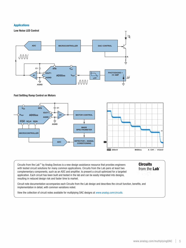
Applications
Low Noise LED Control
A
RFB
IOUT1
AGNDVREFAD55xx
ADC
VDD
AGND
C1
A1
MICROCONTROLLER DAC CONTROL
LPF
PHOTODIODE +I/V AMP
Fast Settling Ramp Control on Motors
RFB
IOUT1
AGND
SCLK SDIN
VREF
SYNC
AD55xx
VDD
AGND
ADC
C1
A1
MICROCONTROLLER
MOTOR CONTROL
MASSSPECTROMETER
DETECTOR + SIGNALCONDITIONING
CH1 200mV M400ns A CH1 412mV
1
Circuits from the Lab™ by Analog Devices is a new design assistance resource that provides engineers with tested circuit solutions for many common applications. Circuits from the Lab pairs at least two complementary components, such as an ADC and amplifier, to present a circuit optimized for a targeted application. Each circuit has been built and tested in the lab and can be easily integrated into designs, resulting in reduced design risk and faster time to market.
Circuit note documentation accompanies each Circuits from the Lab design and describes the circuit function, benefits, and implementation in detail, with common variations noted.
View the collection of circuit notes available for multiplying DAC designs at www.analog.com/circuits.
www.analog.com/multiplyingDAC | 5

Applications
Single-Ended-to-Differential Conditioning
*UNCOMMITTED RESISTOR VERSION
RFB
R1
ROFS
IOUT1
AGND
SCLK SDINSYNC
AD55xxVDD
AGND
C1
A1
A3
A2
MICROCONTROLLER
AC REFERENCE
DIFFERENTIALOUTPUT VOLTAGE
1.5V
1.5V
1.5V
VREFRCOM
C2
A4
1.5V
Fast Settling Ramp Generation and Offset Control
OFFSETDAC
AWGDAC
AD562112-BIT
AD554516-BIT
ADR4233.0V
AGND
C1
A1IOUTA
IOUTB
VREFA
RFBA
VREFB
VDD
VOUT
GENERATED WAVEFORM
0V
Circuit Note CN-0143, Single-Ended-to-Differential Converters for Voltage Output and Current Output DACs Using the AD8042 Op Amp. www.analog.com/CN0143
For more information on ADI’s multiplying DAC portfolio see www.analog.com/multiplyingDAC.
6 | Multiplying DACs
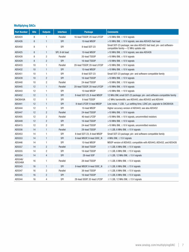
Multiplying DACs
Part Number Bits Outputs Interface Package Comments
AD5424 8 1 Parallel 16-lead TSSOP, 20-lead LFCSP >10 MHz BW, ±10 V signals
AD5426 8 1 SPI 10-lead MSOP >10 MHz BW, ±10 V signals; see also AD5425 fast load
AD5450 8 1 SPI 8-lead SOT-23Small SOT-23 package; see also AD5425 fast load; pin- and software-compatible family —12 MHz update rate
AD5425 8 1 SPI, 8-bit load 10-lead MSOP >10 MHz BW, ±10 V signals; see also AD5426
AD5428 8 2 Parallel 20-lead TSSOP >10 MHz BW, ±10 V signals
AD5429 8 2 SPI 16-lead TSSOP >10 MHz BW, ±10 V signals
AD5433 10 1 Parallel 20-lead TSSOP, 20-lead LFCSP >10 MHz BW, ±10 V signals
AD5432 10 1 SPI 10-lead MSOP >10 MHz BW, ±10 V signals
AD5451 10 1 SPI 8-lead SOT-23 Small SOT-23 package; pin- and software-compatible family
AD5439 10 2 SPI 16-lead TSSOP >10 MHz BW, ±10 V signals
AD5440 10 2 Parallel 24-lead TSSOP >10 MHz BW, ±10 V signals
AD5445 12 1 Parallel 20-lead TSSOP, 20-lead LFCSP >10 MHz BW, ±10 V signals
AD5443 12 1 SPI 10-lead MSOP >10 MHz BW, ±10 V signals
AD5452 12 1 SPI 8-lead SOT-23, 8-lead MSOP 12 MHz BW, small SOT-23 package; pin- and software-compatible family
DAC8043A 12 1 SPI 8-lead TSSOP >2 MHz bandwidth; see AD5443, also AD5452 and AD5444
AD5441 12 1 SPI 8-lead LFCSP, 8-lead MSOP Low noise, 1 LSB, 1 µs settling time, LDAC pin, upgrade to DAC8043A
AD5444 12 1 SPI 10-lead MSOP Higher accuracy version of AD5443; see also AD5452
AD5447 12 2 Parallel 24-lead TSSOP >10 MHz BW, ±10 V signals
AD5405 12 2 Parallel 40-lead LFCSP >10 MHz BW, ±10 V signals, uncommitted resistors
AD5449 12 2 SPI 16-lead TSSOP >10 MHz BW, ±10 V signals
AD5415 12 2 SPI 24-lead TSSOP >10 MHz BW, ±10 V signals, uncommitted resistors
AD5556 14 1 Parallel 28-lead TSSOP ±1 LSB, 6 MHz BW, ±15 V signals
AD5453 14 1 SPI 8-lead SOT-23, 8-lead MSOP Small SOT-23 package; pin- and software-compatible family
AD5553 14 1 SPI 8-lead MSOP, 8-lead SOIC_N 4 MHz BW, ±15 V signals
AD5446 14 1 SPI 10-lead MSOP MSOP version of AD5453; compatible with AD5443, AD5432, and AD5426
AD5557 14 2 Parallel 38-lead TSSOP ±1 LSB, 6 MHz BW, ±15 V signals
AD5555 14 2 SPI 16-lead TSSOP ±1 LSB, 6 MHz BW, ±15 V signals
AD5554 14 4 SPI 28-lead SOP ±1 LSB, 12 MHz BW, ±15 V signals
AD5546/AD5546A
16 1 Parallel 28-lead TSSOP ±1 LSB, 6 MHz BW, ±15 V signals
AD5543 16 1 SPI 8-lead MSOP, 8-lead SOIC_N ±1 LSB, 6 MHz BW, ±15 V signals
AD5547 16 2 Parallel 38-lead TSSOP ±1 LSB, 6 MHz BW, ±15 V signals
AD5545 16 2 SPI 16-lead TSSOP ±1 LSB, 6 MHz BW, ±15 V signals
AD5544 16 4 SPI 28-lead SSOP, 32-lead LFCSP ±1 LSB, 12 MHz BW, ±15 V signals
www.analog.com/multiplyingDAC | 7
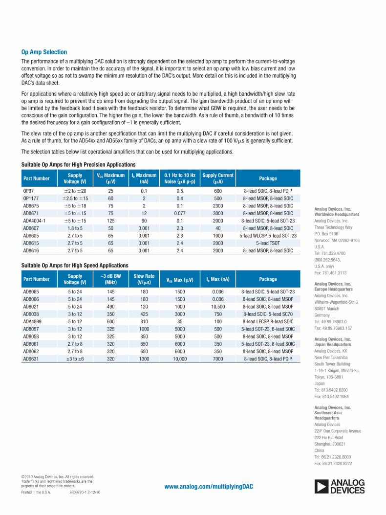
Op Amp SelectionThe performance of a multiplying DAC solution is strongly dependent on the selected op amp to perform the current-to-voltage conversion. In order to maintain the dc accuracy of the signal, it is important to select an op amp with low bias current and low offset voltage so as not to swamp the minimum resolution of the DAC’s output. More detail on this is included in the multiplying DAC’s data sheet.
For applications where a relatively high speed ac or arbitrary signal needs to be multiplied, a high bandwidth/high slew rate op amp is required to prevent the op amp from degrading the output signal. The gain bandwidth product of an op amp will be limited by the feedback load it sees with the feedback resistor. To determine what GBW is required, the user needs to be conscious of the gain configuration. The higher the gain, the lower the bandwidth. As a rule of thumb, a bandwidth of 10 times the desired frequency for a gain configuration of –1 is generally sufficient.
The slew rate of the op amp is another specification that can limit the multiplying DAC if careful consideration is not given. As a rule of thumb, for the AD54xx and AD55xx family of DACs, an op amp with a slew rate of 100 V/µs is generally sufficient.
The selection tables below list operational amplifiers that can be used for multiplying applications.
Suitable Op Amps for High Precision Applications
Part NumberSupply
Voltage (V)VOS Maximum
(𝛍V)IB Maximum
(nA)0.1 Hz to 10 Hz Noise (𝛍V p-p)
Supply Current (𝛍A) Package
OP97 ±2 to ±20 25 0.1 0.5 600 8-lead SOIC, 8-lead PDIP
OP1177 ±2.5 to ±15 60 2 0.4 500 8-lead MSOP, 8-lead SOIC
AD8675 ±5 to ±18 75 2 0.1 2300 8-lead MSOP, 8-lead SOIC
AD8671 ±5 to ±15 75 12 0.077 3000 8-lead MSOP, 8-lead SOIC
ADA4004-1 ±5 to ±15 125 90 0.1 2000 8-lead SOIC, 5-lead SOT-23
AD8607 1.8 to 5 50 0.001 2.3 40 8-lead MSOP, 8-lead SOIC
AD8605 2.7 to 5 65 0.001 2.3 1000 5-lead WLCSP, 5-lead SOT-23
AD8615 2.7 to 5 65 0.001 2.4 2000 5-lead TSOT
AD8616 2.7 to 5 65 0.001 2.4 2000 8-lead MSOP, 8-lead SOIC
Suitable Op Amps for High Speed Applications
Part NumberSupply
Voltage (V)–3 dB BW
(MHz)Slew Rate
(V/𝛍s) VOS Max (𝛍V) IB Max (nA) Package
AD8065 5 to 24 145 180 1500 0.006 8-lead SOIC, 5-lead SOT-23
AD8066 5 to 24 145 180 1500 0.006 8-lead SOIC, 8-lead MSOP
AD8021 5 to 24 490 120 1000 10,500 8-lead SOIC, 8-lead MSOP
AD8038 3 to 12 350 425 3000 750 8-lead SOIC, 5-lead SC70
ADA4899 5 to 12 600 310 35 100 8-lead LFCSP, 8-lead SOIC
AD8057 3 to 12 325 1000 5000 500 5-lead SOT-23, 8-lead SOIC
AD8058 3 to 12 325 850 5000 500 8-lead SOIC, 8-lead MSOP
AD8061 2.7 to 8 320 650 6000 350 5-lead SOT-23, 8-lead SOIC
AD8062 2.7 to 8 320 650 6000 350 8-lead SOIC, 8-lead MSOP
AD9631 ±3 to ±6 320 1300 10,000 7000 8-lead SOIC, 8-lead PDIP
www.analog.com/multiplyingDAC
Analog Devices, Inc.Worldwide HeadquartersAnalog Devices, Inc. Three Technology Way P.O. Box 9106 Norwood, MA 02062-9106 U.S.A. Tel: 781.329.4700 (800.262.5643, U.S.A. only) Fax: 781.461.3113
Analog Devices, Inc. Europe HeadquartersAnalog Devices, Inc. Wilhelm-Wagenfeld-Str. 6 80807 Munich Germany Tel: 49.89.76903.0 Fax: 49.89.76903.157
Analog Devices, Inc. Japan HeadquartersAnalog Devices, KK New Pier Takeshiba South Tower Building 1-16-1 Kaigan, Minato-ku, Tokyo, 105-6891 Japan Tel: 813.5402.8200 Fax: 813.5402.1064
Analog Devices, Inc. Southeast Asia HeadquartersAnalog Devices 22/F One Corporate Avenue 222 Hu Bin Road Shanghai, 200021 China Tel: 86.21.2320.8000 Fax: 86.21.2320.8222
©2010AnalogDevices,Inc.Allrightsreserved.Trademarksandregisteredtrademarksarethepropertyoftheirrespectiveowners.
PrintedintheU.S.A. BR09270-1.2-12/10