There are a pair of small n-type regions just under the drain & source electrodes.
If apply a +ve voltage to gate, will push away the ‘holes’ inside the p-type substrate and attracts the moveable electrons in the n-type regions under the source & drain electrodes.
The gate electrode is placed on top of a very thin insulating layer.
Increasing the +ve gate
voltage pushes the p-
type holes further away
and enlarges the
thickness of the created
channel.
As a result increases
the amount of current
which can go from
source to drain — this is
why this kind of
transistor is called an
Enhancement mode
device.


A MOSFET device is considered to be short when
the channel length is the same order of as the
channel length L is reduced to increase both the
operation speed and the number of components
per chip, the so-called short-channel effects
arise.

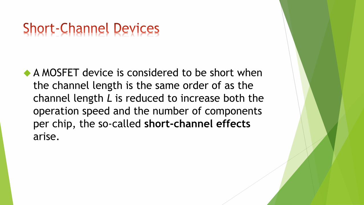
The short-channel effects are attributed to two physical phenomena:
A) The limitation imposed on electron drift characteristics in the channel,
B) The modification of the threshold voltage due to the shortening channel
length.
In particular five different short-channel effects can be distinguished:
1. Drain-induced barrier lowering and “Punch through”
2. Surface scattering
3. Velocity saturation
4. Impact ionization
5. Hot electrons

When the depletion regions surrounding the drain
extends to the source, so that the two depletion
layer merge, punch trough occurs. Punch through
can be minimized with thinner oxides, larger
substrate doping, shallower junctions, and
obviously with longer channels.

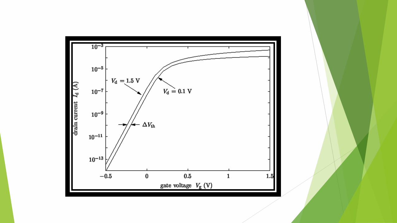
In small-geometry MOSFETs, the potential barrier
is controlled by both the gate-to-source voltage
VGS and the drain-to-source voltage VDS. If the
drain voltage is increased, the potential barrier in
the channel decreases, leading to drain-induced
barrier lowering (DIBL). The reduction of the
potential barrier eventually allows electron flow
between the source and the drain, even if the
gate-to-source voltage is lower than the threshold
voltage.

ECE 663
Punch-Through
rj
Ws
xo
rj
WD
L
rj
Ws
xo
rj
WD
L
+VD
++VD
n-p-n BJT
S&D depletions touch – punch through
e-


As the channel length becomes smaller due to the
lateral extension of the depletion layer into the
channel region, the longitudinal electric field
component increases, and the surface mobility
becomes field-dependent. Since the carrier
transport in a MOSFET is confined within the
narrow inversion layer, and the surface scattering
causes reduction of the mobility, the electrons
move with great difficulty parallel to the
interface, so that the average surface mobility is
about half as much as that of the bulk mobility.

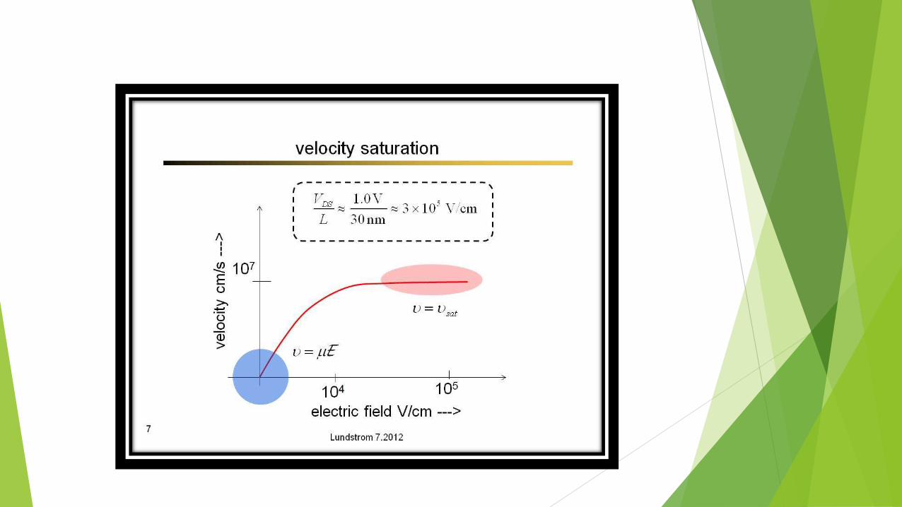
The performance short-channel devices is also
affected by velocity saturation, which reduces
the trans conductance in the saturation mode. At
low ey, the electron drift velocity Vde in the
channel varies linearly with the electric field
intensity. However, as ey increases the drift
velocity tends to increase more slowly, and
approaches a saturation value.
The drain current is limited by velocity saturation
instead of pinch off. This occurs in short channel
devices when the dimensions are scaled without
lowering the bias voltages.
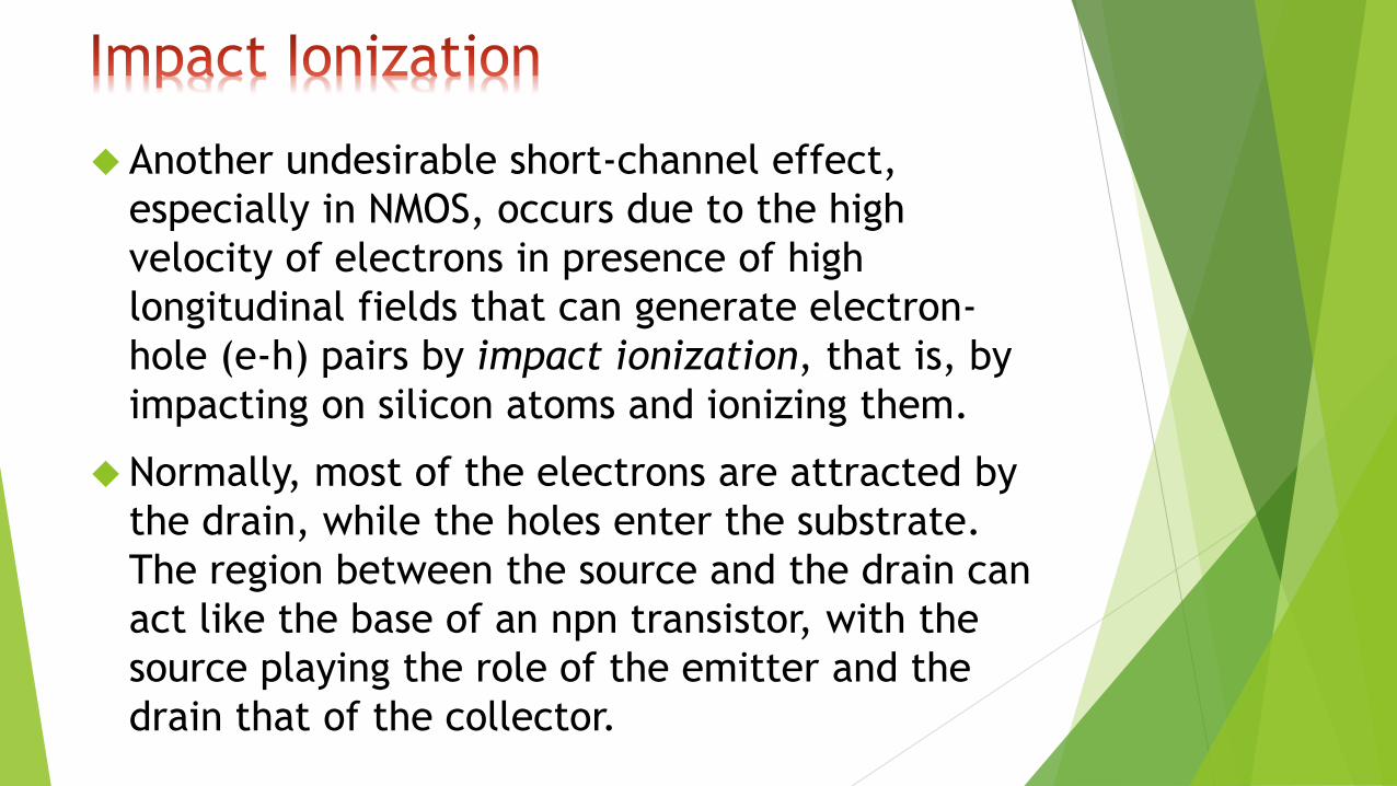
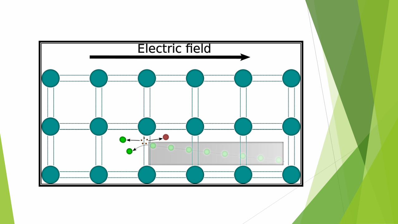
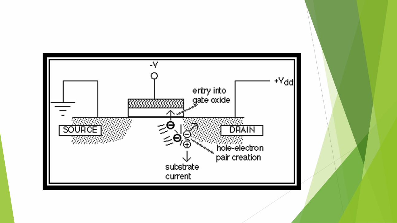
Another undesirable short-channel effect,
especially in NMOS, occurs due to the high
velocity of electrons in presence of high
longitudinal fields that can generate electron-
hole (e-h) pairs by impact ionization, that is, by
impacting on silicon atoms and ionizing them.
Normally, most of the electrons are attracted by
the drain, while the holes enter the substrate.
The region between the source and the drain can
act like the base of an npn transistor, with the
source playing the role of the emitter and the
drain that of the collector.

If the aforementioned holes are collected by the
source, and the corresponding hole current
creates a voltage drop in the substrate material.
Then electrons can be injected from the source to
the substrate, similar to the injection of electrons
from the emitter to the base. They can gain
enough energy as they travel toward the drain to
create new eh pairs. The situation can worsen if
some electrons generated due to high fields
escape the drain field to travel into the substrate,
thereby affecting other devices on a chip.

Another problem, related to high electric fields,
is caused by so-called hot electrons. This high
energy electrons can enter the oxide, where they
can be trapped, giving rise to oxide charging that
can accumulate with time and degrade the device
performance by increasing VT and affect
adversely the gate’s control on the drain current.


SCE are governed by complex physical phenomena that can be mainly related to the Influence of both vertical and horizontal electric field components on the flow of the electrons in the channel
Usually SCE interacts the one with the other
SCE should be carefully considered in order to evaluate their impact on the general behaviour of the device, both for short-term and long-term