Model No.TM070RVHG01-00
The information contained herein is the exclusive property of TIANMA MICRO-ELECTRONICS Corporation and shall not be distributed, reproduced, or disclosed in whole or in part without prior written permission of TIANMA MICRO-ELECTRONICS Corporation.
Page 1 of 25
MODEL NO. : TM070RVHG01-01
ISSUED DATE: 2015/06/30
VERSION : V1.4
■Preliminary Specification □Final Product Specification
Customer :
Approved by Notes
TIANMA Confirmed :
Prepared by Checked by Approved by
Fen He Fan Jiang Feng Qin
This technical specification is subjected to change without notice
Model No.TM070RVHG01-00
The information contained herein is the exclusive property of TIANMA MICRO-ELECTRONICS Corporation and shall not be distributed, reproduced, or disclosed in whole or in part without prior written permission of TIANMA MICRO-ELECTRONICS Corporation.
Page 2 of 25
Table of Contents
Table of Contents ................................................................................................................................. 2
Record of Revision............................................................................................................................... 3
1 General Specifications .................................................................................................................. 4
2 Input/Output Terminals .................................................................................................................. 5
3 Absolute Maximum Ratings .......................................................................................................... 7
4 Electrical Characteristics .............................................................................................................. 8
5 Timing Chart ................................................................................................................................ 10
6 Optical Characteristics ................................................................................................................ 13
7 Environmental / Reliability Test ................................................................................................... 17
8 Mechanical Drawing.................................................................................................................... 18
9 Packing Drawing ......................................................................................................................... 19 10 Product Inspection Criteria.......................................................................................................... 20 11 Precautions for Use of LCD Modules ......................................................................................... 25
Model No.TM070RVHG01-00
The information contained herein is the exclusive property of TIANMA MICRO-ELECTRONICS Corporation and shall not be distributed, reproduced, or disclosed in whole or in part without prior written permission of TIANMA MICRO-ELECTRONICS Corporation.
Page 3 of 25
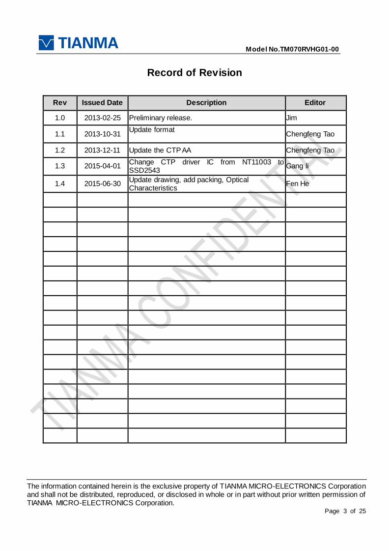
Record of Revision
Rev Issued Date Description Editor
1.0 2013-02-25 Preliminary release. Jim
1.1 2013-10-31 Update format
Chengfeng Tao
1.2 2013-12-11 Update the CTP AA Chengfeng Tao
1.3 2015-04-01 Change CTP driver IC from NT11003 to SSD2543
Gang li
1.4 2015-06-30 Update drawing, add packing, Optical Characteristics
Fen He
Model No.TM070RVHG01-00
The information contained herein is the exclusive property of TIANMA MICRO-ELECTRONICS Corporation and shall not be distributed, reproduced, or disclosed in whole or in part without prior written permission of TIANMA MICRO-ELECTRONICS Corporation.
Page 4 of 25
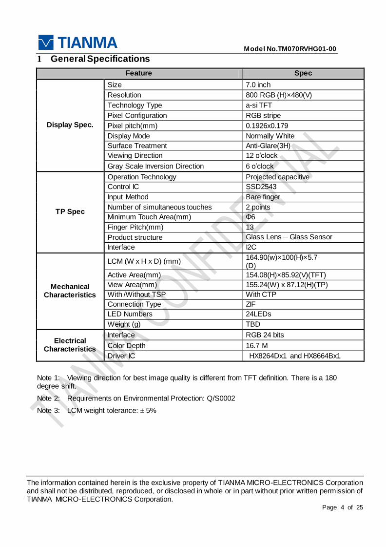
1 General Specifications
Feature Spec
Display Spec.
Size 7.0 inch
Resolution 800 RGB (H)×480(V)
Technology Type a-si TFT
Pixel Configuration RGB stripe
Pixel pitch(mm) 0.1926x0.179
Display Mode Normally White
Surface Treatment Anti-Glare(3H)
Viewing Direction 12 o’clock
Gray Scale Inversion Direction 6 o’clock
TP Spec
Operation Technology Projected capacitive
Control IC SSD2543
Input Method Bare finger
Number of simultaneous touches 2 points
Minimum Touch Area(mm) Φ6
Finger Pitch(mm) 13
Product structure Glass Lens-Glass Sensor
Interface I2C
Mechanical Characteristics
LCM (W x H x D) (mm) 164.90(w)×100(H)×5.7 (D)
Active Area(mm) 154.08(H)×85.92(V)(TFT)
View Area(mm) 155.24(W) x 87.12(H)(TP)
With /Without TSP With CTP
Connection Type ZIF
LED Numbers 24LEDs
Weight (g) TBD
Electrical Characteristics
Interface RGB 24 bits
Color Depth 16.7 M
Driver IC HX8264Dx1 and HX8664Bx1
Note 1: Viewing direction for best image quality is different from TFT definition. There is a 180 degree shift.
Note 2: Requirements on Environmental Protection: Q/S0002
Note 3: LCM weight tolerance: ± 5%
Model No.TM070RVHG01-00
The information contained herein is the exclusive property of TIANMA MICRO-ELECTRONICS Corporation and shall not be distributed, reproduced, or disclosed in whole or in part without prior written permission of TIANMA MICRO-ELECTRONICS Corporation.
Page 5 of 25
2 Input/Output Terminals
2.1 TFT CN1 pin assignment
Connector type: FH28-60S-0.5SH
PIN Symbol I/O Description Remark
1 VLED+ P Led anode
2 VLED+ P Led anode
3 VLED- P Led cathode
4 VLED- P Led cathode
5 GND P Ground
6 VCOM P Common voltage input
7 VCC P Digital power supply
8 MODE I DE/SYNC mode select. H:DE mode, L:SYNC mode
9 DE I Data enable signal, active high to enable data,if not used,please pull low
10 VSYNC I Vertical sync input, negative polarity,if not used,please pull High
11 HSYNC I Horizontal sync input, negative polarity,if not used,please pull High
12 B7 I Blue data(MSB)
13 B6 I Blue data
14 B5 I Blue data
15 B4 I Blue data
16 B3 I Blue data
17 B2 I Blue data
18 B1 I Blue data
19 B0 I Blue data(LSB)
20 G7 I Green data(MSB)
21 G6 I Green data
22 G5 I Green data
23 G4 I Green data
24 G3 I Green data
25 G2 I Green data
26 G1 I Green data
27 G0 I Green data(LSB)
28 R7 I Red data(MSB)
29 R6 I Red data
30 R5 I Red data
31 R4 I Red data
32 R3 I Red data
33 R2 I Red data
34 R1 I Red data
35 R0 I Red data(LSB)
36 GND P Ground
37 DCLK I Clock for input data
38 GND P Ground
Model No.TM070RVHG01-00
The information contained herein is the exclusive property of TIANMA MICRO-ELECTRONICS Corporation and shall not be distributed, reproduced, or disclosed in whole or in part without prior written permission of TIANMA MICRO-ELECTRONICS Corporation.
Page 6 of 25
39 LR I Source left or right sequence control
40 UD I Gate up or down scan control
41 VGH P Positive power of TFT
42 VGL P Negative power of TFT
43 AVDD P Analog power supply
44 RESET I Global reset pin
45 NC NC
46 VCOM P
47 DITHB I Dithering setting. H: 6bit resolution, L: 8bit resolution
48 GND P Ground
49 NC NC
50 NC NC
Note1:I/O definition I---Input, O---Output, P--- Power/Ground, NC-No connection
Table 2.1 terminal pin assignments
2.2 U/D R/L Function Description
Scan control input Scanning direction
UD LR
GND VCC Up to down, left to right
VCC GND Down to up, right to left
GND GND Up to down, right to left
VCC VCC Down to up, left to right
2.3 TP pin assignment Connector type: FH19S-10S-0.5SH
Pin No. Symbol I/O Description Remark
1 SCL I I2C clock input
2 SDA I/O I2C data input and output
3 GND P Ground
4 GND P Ground
5 ATTN I/O External interrupt to the host
6 GND P Ground
7 VPP I/O External interrupt from the host
8 VDD P CTP power supply
9 GND P Ground
10 GND P Ground

Model No.TM070RVHG01-00
The information contained herein is the exclusive property of TIANMA MICRO-ELECTRONICS Corporation and shall not be distributed, reproduced, or disclosed in whole or in part without prior written permission of TIANMA MICRO-ELECTRONICS Corporation.
Page 7 of 25
3 Absolute Maximum Ratings
Ta = 25℃
Item Symbol Min Max Unit Remark
Power Voltage
VDD -0.50 5.00 V
AVDD -0.50 15.00 V
VGH -0.30 42.00 V
VGL -20.0 0.30 V
VGH-VGL -0.30 40.00 V
Backlight Forward Current ILED - 200 mA
Operating Temperature TOPR -20 70 ℃ Note2
Storage Temperature TSTG -30 80 ℃
Table 3.1 absolute maximum rating
Note1: The parameter is for driver IC (gate driver, source driver) only
Note2: 80℃ is the surface temperature of module
Model No.TM070RVHG01-00
The information contained herein is the exclusive property of TIANMA MICRO-ELECTRONICS Corporation and shall not be distributed, reproduced, or disclosed in whole or in part without prior written permission of TIANMA MICRO-ELECTRONICS Corporation.
Page 8 of 25
4 Electrical Characteristics
4.1.1 Driving TFT LCD Panel
Ta = 25℃
Item Symbol Min Typ Max Unit Remark
Voltage for logic circuit VCC 3.00 3.30 3.60 V
Analog Supply Voltage AVDD 9.88 10.4 10.92 V
Gate On Voltage VGG 14.4 16 17.6 V
Gate Off Voltage VEE -7.70 -7.00 -6.30 V
Common Electrode Driving Signal
VCOM 3.93 3.95 3.97 V
Input Signal Voltage
Low Level VIL 0 - 0.3xVCC V
High Level VIH 0.7xVCC - VCC V
Table 4.1 LCD module electrical characteristics
Note1: For different LCM, the value may have a bit of difference. Note2: To test the current dissipation, use “all Black Pattern”.
4.1.2 TFT Driving Backlight
Item Symbol Condition Min Typ Max Unit Remark
Forward Voltage VLED IF=160mA -- 9.6 10.8 V
Note 1 Forward Current IF - - 160 200 mA
Backlight Power Consumption WBL IF=160mA -- 1536 2160 mW
Life Time - IF=160mA 10,000 - - Hrs Note 3
Table 4.1.2 LED backlight characteristics
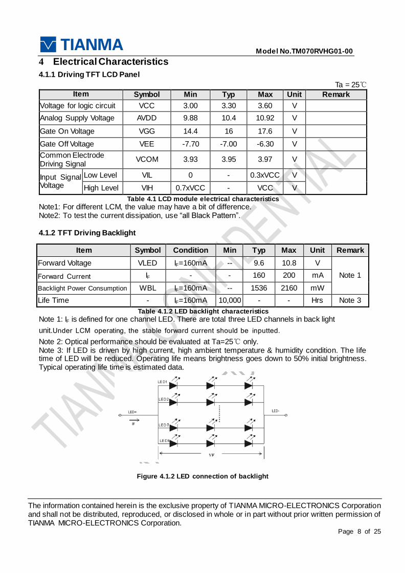
Note 1: IF is defined for one channel LED. There are total three LED channels in back light
unit.Under LCM operating, the stable forward current should be inputted. Note 2: Optical performance should be evaluated at Ta=25℃ only. Note 3: If LED is driven by high current, high ambient temperature & humidity condition. The life time of LED will be reduced. Operating life means brightness goes down to 50% initial brightness. Typical operating life time is estimated data.
Figure 4.1.2 LED connection of backlight

Model No.TM070RVHG01-00
The information contained herein is the exclusive property of TIANMA MICRO-ELECTRONICS Corporation and shall not be distributed, reproduced, or disclosed in whole or in part without prior written permission of TIANMA MICRO-ELECTRONICS Corporation.
Page 9 of 25
4.2 TP DC Characteristics
(TA= 25℃,VDD=3.3V)
Item Min Typ Max Unit Note
power supply voltage 2.7 3.3 3.6 V DC(noise should be under 100mV)
Power supply current -- -- 10 mA
4.3.1 TFT Block Diagram
4.3.2 TP Circuit Block Diagram
Y
TP PANEL
CONTROLLER (with SSD2543
on FPC)
TP PANEL I2C
FPC
7’’ 800RGBx480
CN2
LE
D lig
ht b
ar
Gate
IC
CN1
FPC
HOST
CONTROLLER
Source IC

Model No.TM070RVHG01-00
The information contained herein is the exclusive property of TIANMA MICRO-ELECTRONICS Corporation and shall not be distributed, reproduced, or disclosed in whole or in part without prior written permission of TIANMA MICRO-ELECTRONICS Corporation.
Page 10 of 25
5 Timing Chart
5.1 TFT-LCD Input Timing
VCC=3.3V, GND=0V, Ta=25℃
Parameter Symbol Min Typ Max Unit Remark
DCLK frequency Fclk 28 30.0 40.0 MHz
DCLK cycle time Tcph 25 33.3 36 ns
DCLK pulse width Tcw 40% 50% 60% Tcph
VS setup time Tvst 8 ns
VS hold time Tvhd 8 - - ns
HS setup time Thst 8 ns
HS hold time Thhd 8 - - ns
Data setup time Tdsu 8 ns Data to DCLK
Data hold time Tdhd 8 - - ns Data to DCLK
DE setup time Tesu 8 - - ns
DE hold time Tehd 8 - - ns
Input Clock and Data timing Diagram:
Model No.TM070RVHG01-00
The information contained herein is the exclusive property of TIANMA MICRO-ELECTRONICS Corporation and shall not be distributed, reproduced, or disclosed in whole or in part without prior written permission of TIANMA MICRO-ELECTRONICS Corporation.
Page 11 of 25
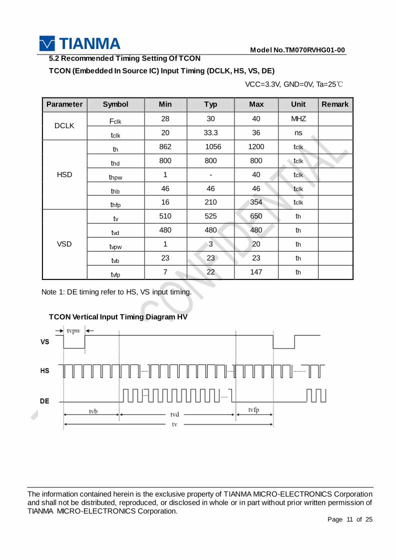
5.2 Recommended Timing Setting Of TCON
TCON (Embedded In Source IC) Input Timing (DCLK, HS, VS, DE)
VCC=3.3V, GND=0V, Ta=25℃
Parameter Symbol Min Typ Max Unit Remark
DCLK Fclk 28 30 40 MHZ
tclk 20 33.3 36 ns
HSD
th 862 1056 1200 tclk
thd 800 800 800 tclk
thpw 1 - 40 tclk
thb 46 46 46 tclk
thfp 16 210 354 tclk
VSD
tv 510 525 650 th
tvd 480 480 480 th
tvpw 1 3 20 th
tvb 23 23 23 th
tvfp 7 22 147 th
Note 1: DE timing refer to HS, VS input timing.
TCON Vertical Input Timing Diagram HV
Model No.TM070RVHG01-00
The information contained herein is the exclusive property of TIANMA MICRO-ELECTRONICS Corporation and shall not be distributed, reproduced, or disclosed in whole or in part without prior written permission of TIANMA MICRO-ELECTRONICS Corporation.
Page 12 of 25
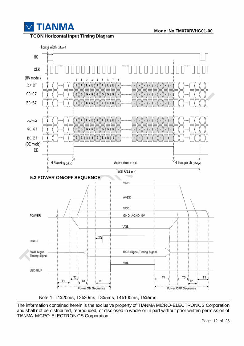
TCON Horizontal Input Timing Diagram
5.3 POWER ON/OFF SEQUENCE
Note 1: T1≥20ms, T2≥20ms, T3≥5ms, T4≥100ms, T5≥5ms.
Model No.TM070RVHG01-00
The information contained herein is the exclusive property of TIANMA MICRO-ELECTRONICS Corporation and shall not be distributed, reproduced, or disclosed in whole or in part without prior written permission of TIANMA MICRO-ELECTRONICS Corporation.
Page 13 of 25
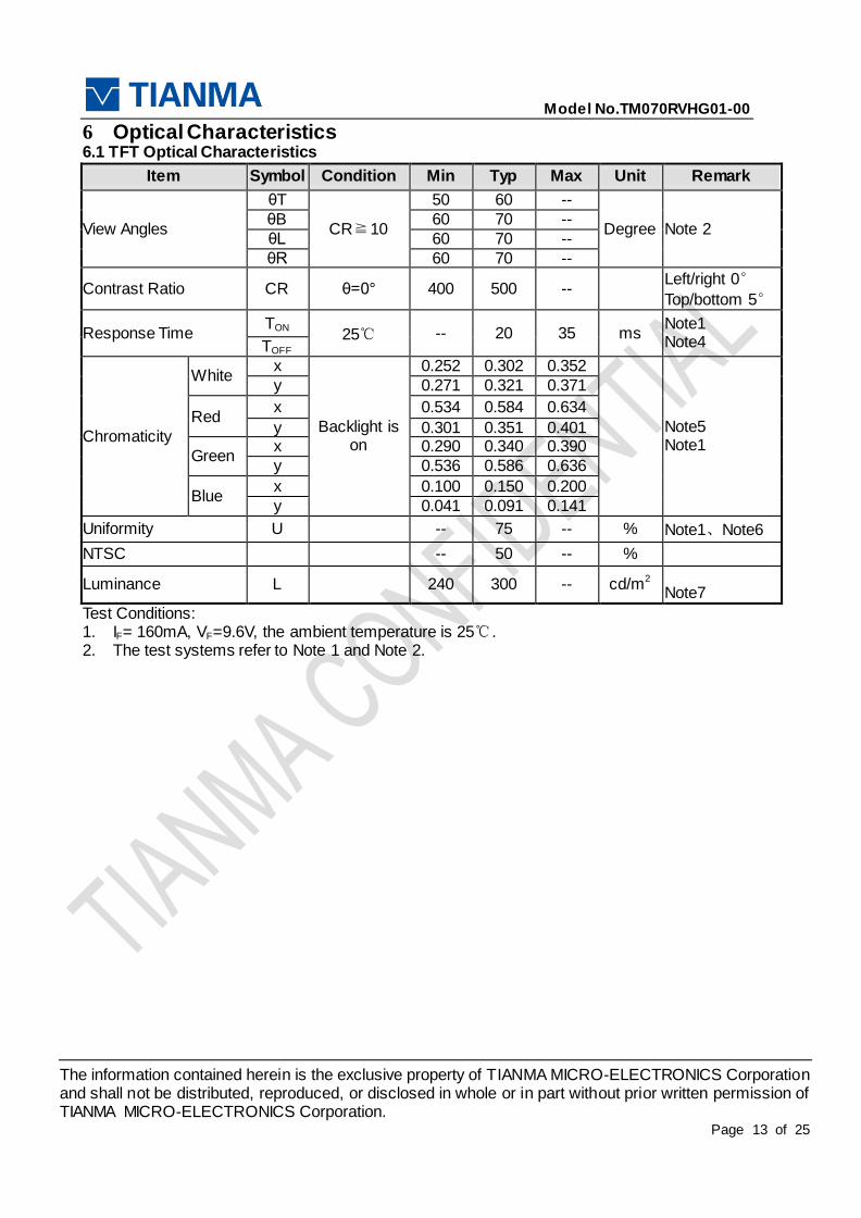
6 Optical Characteristics 6.1 TFT Optical Characteristics
Item Symbol Condition Min Typ Max Unit Remark
View Angles
θT
CR≧10
50 60 --
Degree Note 2 θB 60 70 --
θL 60 70 --
θR 60 70 --
Contrast Ratio CR θ=0° 400 500 -- Left/right 0°
Top/bottom 5°
Response Time TON
25℃ -- 20 35 ms Note1 Note4 TOFF
Chromaticity
White x
Backlight is on
0.252 0.302 0.352
Note5 Note1
y 0.271 0.321 0.371
Red x 0.534 0.584 0.634
y 0.301 0.351 0.401
Green x 0.290 0.340 0.390
y 0.536 0.586 0.636
Blue x 0.100 0.150 0.200
y 0.041 0.091 0.141
Uniformity U -- 75 -- % Note1、Note6
NTSC -- 50 -- %
Luminance L 240 300 -- cd/m2 Note7
Test Conditions: 1. IF= 160mA, VF=9.6V, the ambient temperature is 25℃. 2. The test systems refer to Note 1 and Note 2.

Model No.TM070RVHG01-00
The information contained herein is the exclusive property of TIANMA MICRO-ELECTRONICS Corporation and shall not be distributed, reproduced, or disclosed in whole or in part without prior written permission of TIANMA MICRO-ELECTRONICS Corporation.
Page 14 of 25
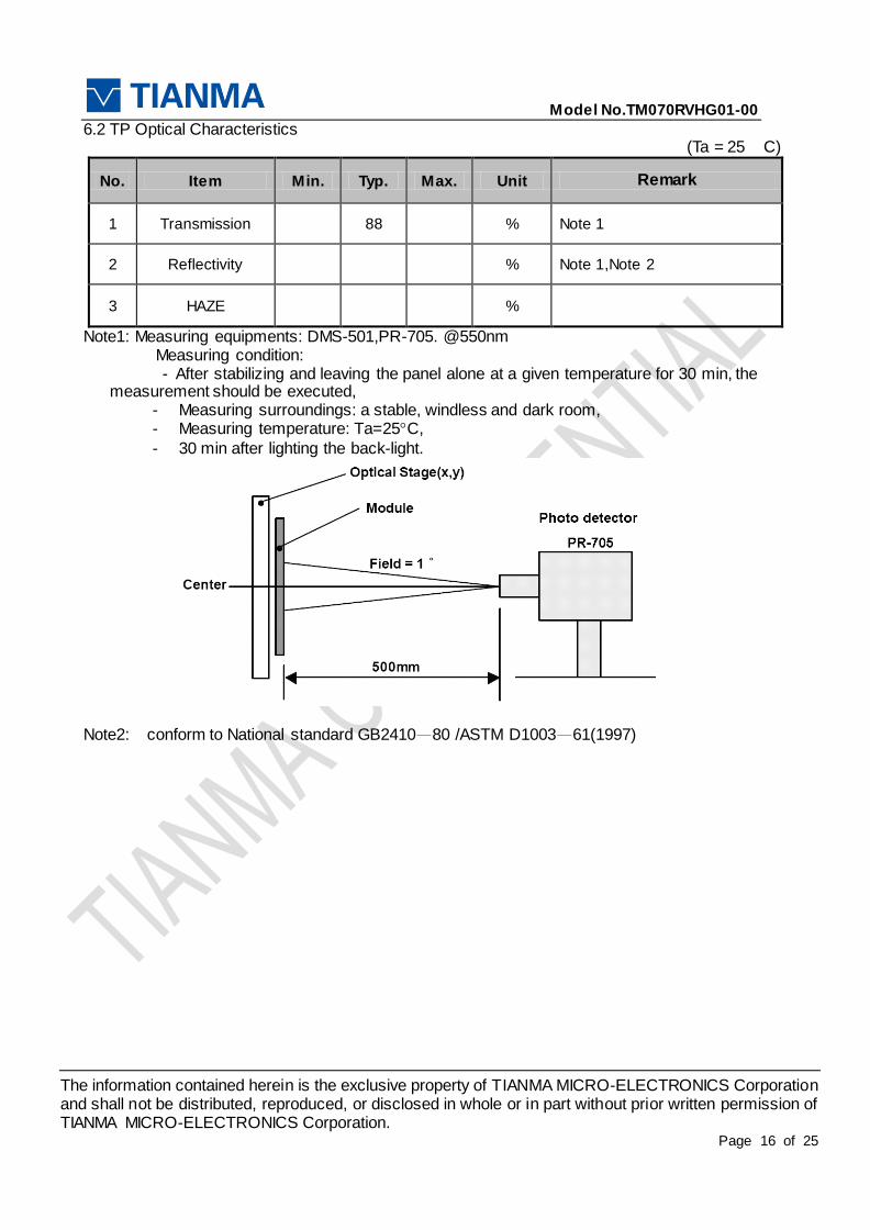
Note 1: Definition of optical measurement system.
The optical characteristics should be measured in dark room. After 5 Minutes operation, the optical properties are measured at the center point of the LCD screen. All input terminals LCD panel must be ground when measuring the center area of the panel.
Note 2: Definition of viewing angle range and measurement system.
viewing angle is measured at the center point of the LCD by CONOSCOPE(ergo-80)。
Note 3: Definition of contrast ratio
“White state “: The state is that the LCD should drive by Vwhite.
“Black state”: The state is that the LCD should drive by Vblack.
Item Photo detector Field
Contrast Ratio
SR-3A 1° Luminance
Chromaticity
Lum Uniformity
Response Time BM-7A 2°
500mm
Photo detector
Field
LCD Panel TFT-LCD Module
The center of the screen
Model No.TM070RVHG01-00
The information contained herein is the exclusive property of TIANMA MICRO-ELECTRONICS Corporation and shall not be distributed, reproduced, or disclosed in whole or in part without prior written permission of TIANMA MICRO-ELECTRONICS Corporation.
Page 15 of 25
Vwhite: To be determined Vblack: To be determined.
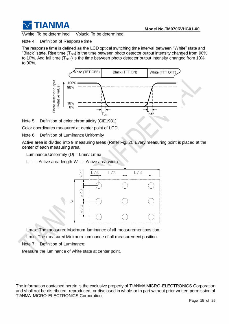
Note 4: Definition of Response time
The response time is defined as the LCD optical switching time interval between “White” state and “Black” state. Rise time (TON) is the time between photo detector output intensity changed from 90% to 10%. And fall time (TOFF) is the time between photo detector output intensity changed from 10% to 90%.
Note 5: Definition of color chromaticity (CIE1931)
Color coordinates measured at center point of LCD.
Note 6: Definition of Luminance Uniformity
Active area is divided into 9 measuring areas (Refer Fig. 2). Every measuring point is placed at the center of each measuring area.
Luminance Uniformity (U) = Lmin/ Lmax
L-------Active area length W----- Active area width
Lmax: The measured Maximum luminance of all measurement position.
Lmin: The measured Minimum luminance of all measurement position.
Note 7: Definition of Luminance:
Measure the luminance of white state at center point.
Model No.TM070RVHG01-00
The information contained herein is the exclusive property of TIANMA MICRO-ELECTRONICS Corporation and shall not be distributed, reproduced, or disclosed in whole or in part without prior written permission of TIANMA MICRO-ELECTRONICS Corporation.
Page 16 of 25
6.2 TP Optical Characteristics (Ta = 25 C)
No. Item Min. Typ. Max. Unit Remark
1 Transmission 88 % Note 1
2 Reflectivity % Note 1,Note 2
3 HAZE %
Note1: Measuring equipments: DMS-501,PR-705. @550nm Measuring condition:
- After stabilizing and leaving the panel alone at a given temperature for 30 min, the measurement should be executed,
- Measuring surroundings: a stable, windless and dark room, - Measuring temperature: Ta=25C,
- 30 min after lighting the back-light.
Note2: conform to National standard GB2410—80 /ASTM D1003—61(1997)
Model No.TM070RVHG01-00
The information contained herein is the exclusive property of TIANMA MICRO-ELECTRONICS Corporation and shall not be distributed, reproduced, or disclosed in whole or in part without prior written permission of TIANMA MICRO-ELECTRONICS Corporation.
Page 17 of 25
7 Environmental / Reliability Test
No Test Item Condition Remarks
1 High Temperature Operation
Ta = +70℃, 240 hours Note1,Note6,Note7 IEC60068-2-1,GB2423.2
2 Low Temperature Operation
Ta = -20℃, 240 hours Note1, Note7,IEC60068-2-1 GB2423.1
3 High Temperature Storage
Ta = +80℃, 240 hours Note1, Note7,Note8 IEC60068-2-1 GB2423.2
4 Low Temperature Storage
Ta = -30℃, 240 hours Note1, Note7,EC60068-2-1 GB2423.1
5 High Temperature & Humidity Storage
Ta=+65℃、RH=90%, 240 hours Note1,Note3, Note4,Note7 IEC60068-2-78 GB/T2423.3
6 Thermal Shock/ Solder Joint Life Test
-30℃(30min)⇔80℃(30min),Change
Time:5min,100cycle
Note1,Note9 Start with cold temperature End with high temperature, IEC60068-2-14,GB2423.22
12 ESD
C=150pF、R=330Ω
Air: ±8KV Contact:±8KV 5times
(Environment:15℃~35℃, 30%~60%.86Kpa~106Kpa)
Note2,Note5, IEC61000-4-2 GB/T17626.2
13 Shock Test Half Sine Wave 100G ,6ms,±X,±Y,±Z 3times for each direction
Note2
14 Drop Test(package state)
Height:60cm, 1corner,3edges,6surfaces
Note2,IEC60068-2-32 GB/T2423.8
Note1: Ts is the temperature of panel’s surface.
Note2: Ta is the ambient temperature of sample.
Note3: Before cosmetic and function test, the product must have enough recovery time, at least 2 hours at room temperature.
Note 4: In the standard condition, there shall be no practical problem that may affect the display function. After the reliability test, the product only guarantees operation, but don’t guarantee all of the cosmetic specification.
Model No.TM070RVHG01-00
The information contained herein is the exclusive property of TIANMA MICRO-ELECTRONICS Corporation and shall not be distributed, reproduced, or disclosed in whole or in part without prior written permission of TIANMA MICRO-ELECTRONICS Corporation.
Page 18 of 25
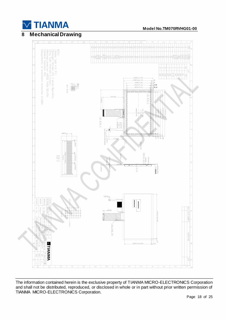
8 Mechanical Drawing
Model No.TM070RVHG01-00
The information contained herein is the exclusive property of TIANMA MICRO-ELECTRONICS Corporation and shall not be distributed, reproduced, or disclosed in whole or in part without prior written permission of TIANMA MICRO-ELECTRONICS Corporation.
Page 19 of 25
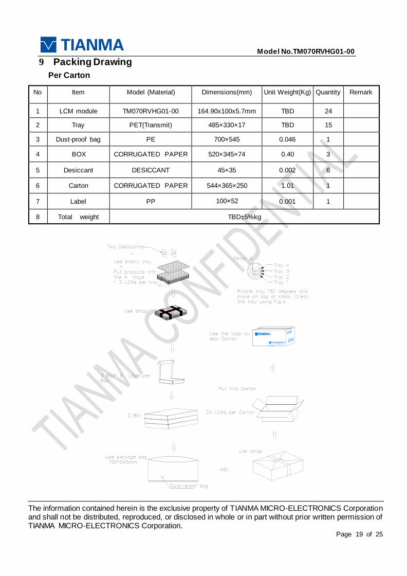
9 Packing Drawing
Per Carton
No Item Model (Material) Dimensions(mm) Unit Weight(Kg) Quantity Remark
1 LCM module TM070RVHG01-00 164.90x100x5.7mm TBD 24
2 Tray PET(Transmit) 485×330×17 TBD 15
3 Dust-proof bag PE 700×545 0.046 1
4 BOX CORRUGATED PAPER 520×345×74 0.40 3
5 Desiccant DESICCANT 45×35 0.002 6
6 Carton CORRUGATED PAPER 544×365×250 1.01 1
7 Label PP 100×52 0.001 1
8 Total weight TBD±5%kg

Model No.TM070RVHG01-00
The information contained herein is the exclusive property of TIANMA MICRO-ELECTRONICS Corporation and shall not be distributed, reproduced, or disclosed in whole or in part without prior written permission of TIANMA MICRO-ELECTRONICS Corporation.
Page 20 of 25
Viewing Area
X1 X2
Y1
Y2
Figure 2
B zone
Active Area(AA)
A zone: Viewing Area(VA)
10 Product Inspection Criteria
10.1 Classification of defects
Major defects (MA): A major defect refers to a defect that may substantially degrade
usability for product applications, including all functional defects(such as no display, abnormal display, open or missing segment, short circuit, missing component), outline
dimension beyond the drawing, progressive defects and those affecting reliability. Minor defects (MI): A minor defect refers to a defect which is not considered to be able
to substantially degrade the product application or a defect that deviates from existing
standards almost unrelated to the effective use of the product or its operation, such as black spot, white spot, bright spot, pinhole, black line, white line, contrast variation, glass
defect, polarizer defect, etc.
10.2 Definition of inspection range For dot defect of TFT LCD which is not
smaller than 3 inches, dividing three areas to make a judgment (according to figure 1).
A area : center of viewing area B area : periphery of viewing area C area : Outside viewing area
For other defects, dividing two areas to make a judgment (according figure 2).
A zone : Inside Viewing area B zone : Outside Viewing area X1(A.A~V.A): 0mm X2(A.A~V.A):
0mm Y1(A.A~V.A): 0mm Y2(A.A~V.A):
0mm
10.3 Inspection items and general notes
General notes
①Should any defects which are not specified in this standard happen, additional standard
shall be determined by mutual agreement between customer and TIANMA. ②Viewing area should be the area which TIANMA guarantees. ③Limit sample should be prior to this Inspection standard.
④Viewing judgment should be under static pattern. ⑤Inspection conditions
Inspection distance: 250 mm (from the sample) Temperature : 25±5 ºC
Inspection angle : 45 degrees in 12 o′clock direction (all defects in viewing area should be inspected from this direction)
Inspection items
Pinhole, Bright spot, Black spot, White spot, Black line, White
Line, Foreign particle, Bubble
The color of a small area is different from the remainder. The phenomenon doesn’t change with
voltage
Contrast variation The color of a small area is different from the remainder. The phenomenon changes with voltage
Polarizer defect Scratch, Dirt, Particle, Bubble on polarizer or between polarizer and glass
Dot defect (TFT LCD) The pixel appears bright or dark abnormally when
display
Figure 1

Model No.TM070RVHG01-00
The information contained herein is the exclusive property of TIANMA MICRO-ELECTRONICS Corporation and shall not be distributed, reproduced, or disclosed in whole or in part without prior written permission of TIANMA MICRO-ELECTRONICS Corporation.
Page 21 of 25
b
a
Φ=(a+b)/2(mm)
W: Width
L:Length(mm
)
a
b
Φ=(a+b)/2(mm)
Functional defect No display, Abnormal display, Open or missing
segment, Short circuit, False viewing direction
Glass defect Glass crack, Shaved corner of glass, Surplus glass
PCB defect Components assembly defect
10.4 Outgoing Inspection level
Outgoing Inspection standard
Inspection conditions Inspection
Min. Max. Unit IL AQL
Major Defects See 9.3 general notes See 9.5 II 0.65
Minor Defects See 9.3 general notes See 9.5 II 1.5
Note:Sampling standard conforms to GB2828
10.5 Inspection Items and Criteria
Inspection items Judgment standard
Category Acceptable number
A zone B zone
1
Black spot, White spot, Bright Spot, Pinhole, Foreign Particle, Particle in or on glass, Scratch on glass
A Φ≦0.10 Neglected
Neglected
B 0.10<Φ≦0.15 2
C 0.15<Φ≦0.20 1
D 0.20<Φ 0
Total defective point(B,C) 3
2
Black line, White line, and Particle Between Polarizer and glass, Scratch on glass
A W≦0.01 Neglected
Neglected
B 0.01<W≦0.03
L≦3.0 2
C 0.03<W≦0.05
L≦3.0 1
D 0.05<W 0
Total defective point(B,C) 3
3 Contrast variation
A Φ≦0.2 Neglected
Neglecte
d
B 0.2<Φ≦0.3 2
C 0.3<Φ≦0.4 1
D 0.4<Φ 0
Total defective point(B,C) 3
Model No.TM070RVHG01-00
The information contained herein is the exclusive property of TIANMA MICRO-ELECTRONICS Corporation and shall not be distributed, reproduced, or disclosed in whole or in part without prior written permission of TIANMA MICRO-ELECTRONICS Corporation.
Page 22 of 25
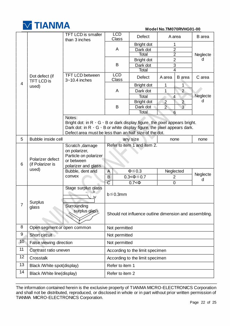
4
Dot defect (if TFT LCD is
used)
TFT LCD is smaller
than 3 inches
LCD Class
Defect A area B area
A Bright dot 1
Neglected
Dark dot 2 Total 2
B Bright dot 2
Dark dot 3 Total 4
TFT LCD between 3~10.4 inches
LCD Class
Defect A area B area C area
A
Bright dot 1 1
Neglected
Dark dot 1 2
Total 4
B
Bright dot 2 2 Dark dot 2 3
Total 6
Notes: Bright dot: in R、G、B or dark display figure, the pixel appears bright. Dark dot: in R、G、B or white display figure, the pixel appears dark.
Defect area must be less than an half size of the dot.
5 Bubble inside cell any size none none
6 Polarizer defect (if Polarizer is
used)
Scratch ,damage
on polarizer, Particle on polarizer or between
polarizer and glass.
Refer to item 1 and item 2.
Bubble, dent and convex
A Φ≦0.3 Neglected Neglecte
d B 0.3<Φ≦0.7 2
C 0.7<Φ 0
7 Surplus glass
Stage surplus glass
b≦0.3mm
Surrounding surplus glass
Should not influence outline dimension and assembling.
8 Open segment or open common Not permitted
9 Short circuit Not permitted
10 False viewing direction Not permitted
11 Contrast ratio uneven According to the limit specimen
12 Crosstalk According to the limit specimen
13 Black /White spot(display) Refer to item 1
14 Black /White line(display) Refer to item 2
b
W
Model No.TM070RVHG01-00
The information contained herein is the exclusive property of TIANMA MICRO-ELECTRONICS Corporation and shall not be distributed, reproduced, or disclosed in whole or in part without prior written permission of TIANMA MICRO-ELECTRONICS Corporation.
Page 23 of 25
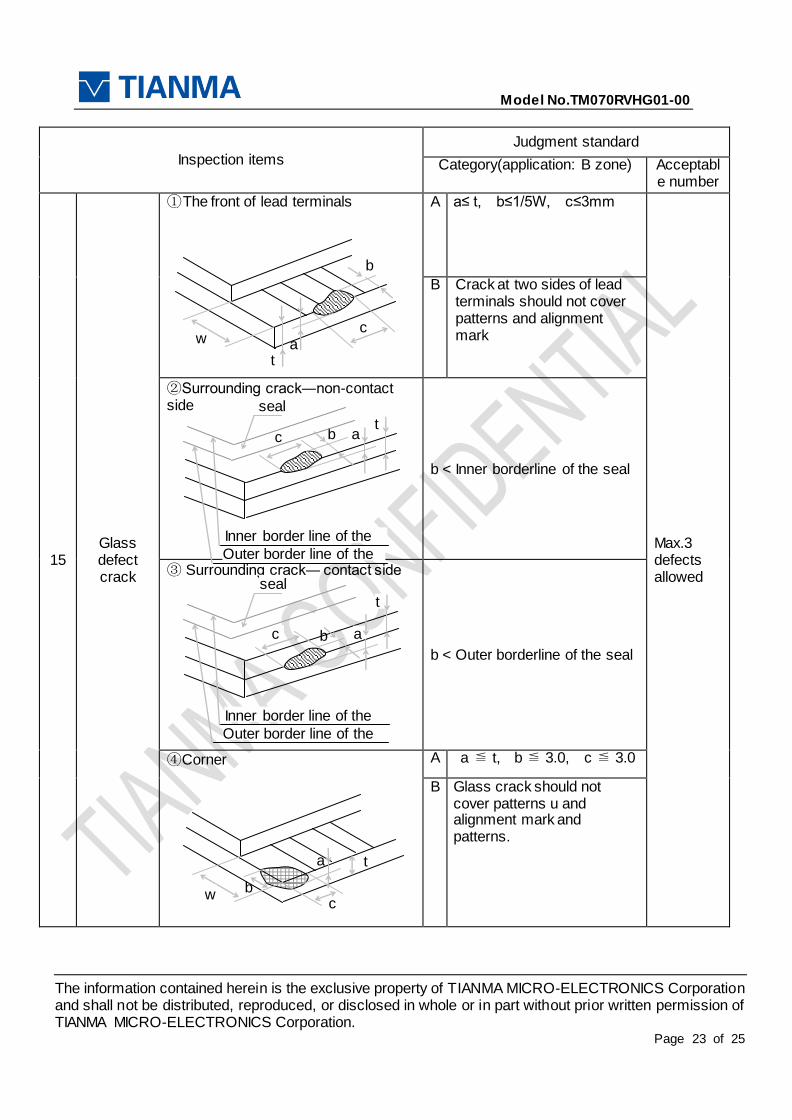
Inspection items
Judgment standard
Category(application: B zone) Acceptable number
15 Glass defect crack
①The front of lead terminals
A a≤ t, b≤1/5W, c≤3mm
Max.3 defects allowed
B Crack at two sides of lead terminals should not cover patterns and alignment mark
②Surrounding crack―non-contact side
b < Inner borderline of the seal
③ Surrounding crack― contact side
b < Outer borderline of the seal
④Corner A a ≦ t, b ≦ 3.0, c ≦ 3.0
B
Glass crack should not cover patterns u and alignment mark and patterns.
c a
b
t
w
seal
Outer border line of the seal
Inner border line of the seal
b a c t
b a
seal
Outer border line of the seal
Inner border line of the seal
c
t
t a
c b w
Model No.TM070RVHG01-00
The information contained herein is the exclusive property of TIANMA MICRO-ELECTRONICS Corporation and shall not be distributed, reproduced, or disclosed in whole or in part without prior written permission of TIANMA MICRO-ELECTRONICS Corporation.
Page 24 of 25
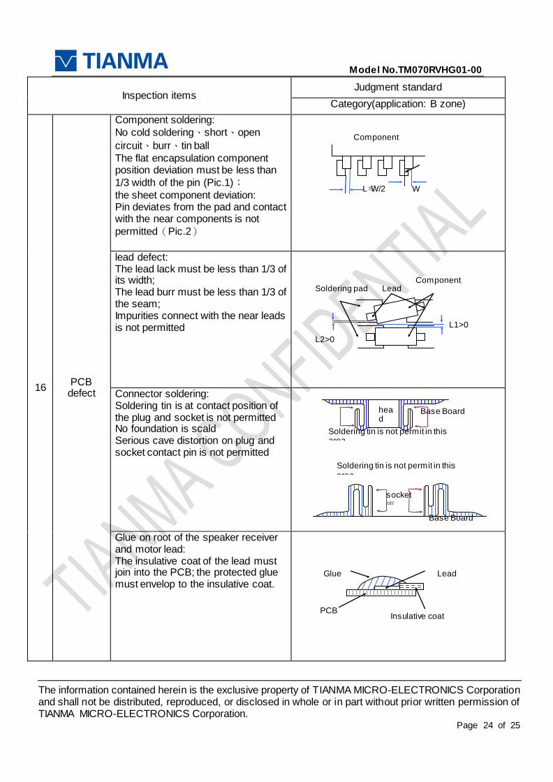
Inspection items Judgment standard
Category(application: B zone)
16 PCB defect
Component soldering:
No cold soldering、short、open
circuit、burr、tin ball
The flat encapsulation component position deviation must be less than
1/3 width of the pin (Pic.1);
the sheet component deviation: Pin deviates from the pad and contact with the near components is not
permitted(Pic.2)
lead defect: The lead lack must be less than 1/3 of its width; The lead burr must be less than 1/3 of the seam; Impurities connect with the near leads is not permitted
Connector soldering: Soldering tin is at contact position of the plug and socket is not permitted No foundation is scald Serious cave distortion on plug and socket contact pin is not permitted
Glue on root of the speaker receiver and motor lead: The insulative coat of the lead must join into the PCB; the protected glue must envelop to the insulative coat.
W L≤W/2
Component
Soldering pad Component
Lead
L1>0
L2>0
Soldering tin is not permit in this area
Base Board head
socket座
Soldering tin is not permit in this area
Base Board
Lead
PCB Insulative coat
Glue
Model No.TM070RVHG01-00
The information contained herein is the exclusive property of TIANMA MICRO-ELECTRONICS Corporation and shall not be distributed, reproduced, or disclosed in whole or in part without prior written permission of TIANMA MICRO-ELECTRONICS Corporation.
Page 25 of 25
11 Precautions for Use of LCD Modules
11.1 Handling Precautions
11.1.1 The display panel is made of glass. Do not subject it to a mechanical shock by dropping it from a high place, etc.
11.1.2 If the display panel is damaged and the liquid crystal substance inside it leaks out, be sure not to get any in your mouth, if the substance comes into contact with your skin or clothes, promptly wash it off using soap and water.
11.1.3 Do not apply excessive force to the display surface or the adjoining areas since this may cause the color tone to vary.
11.1.4 The polarizer covering the display surface of the LCD module is soft and easily scratched. Handle this polarizer carefully.
11.1.5 If the display surface is contaMinated, breathe on the surface and gently wipe it with a soft dry cloth. If still not completely clear, moisten cloth with one of the following solvents:
- Isopropyl alcohol
- Ethyl alcohol
Solvents other than those mentioned above may damage the polarizer. Especially, do not use the following:
- Water
- Ketone
- Aromatic solvents
11.1.6 Do not attempt to disassemble the LCD Module.
11.1.7 If the logic circuit power is off, do not apply the input signals.
11.1.8 To prevent destruction of the elements by static electricity, be careful to maintain an optimum work environment.
11.1.8.1 Be sure to ground the body when handling the LCD Modules.
11.1.8.2 Tools required for assembly, such as soldering irons, must be properly ground.
11.1.8.3 To reduce the amount of static electricity generated, do not conduct assembly and other work under dry conditions.
11.1.8.4 The LCD Module is coated with a film to protect the display surface. Be care when peeling off this protective film since static electricity may be generated.
11.2 Storage precautions
11.2.1 When storing the LCD modules, avoid exposure to direct sunlight or to the light of fluorescent lamps.
11.2.2 The LCD modules should be stored under the storage temperature range. If the LCD modules will be stored for a long time, the recommend condition is:
Temperature : 0℃ ~ 40℃ Relatively humidity: ≤80%
11.2.3 The LCD modules should be stored in the room without acid, alkali and harmful gas.
11.3 Transportation Precautions
11.3.1 The LCD modules should be no falling and violent shocking during transportation, and also should avoid excessive press, water, damp and sunshine.


![4P008-00 03 COG Driv~[1] - Glyn Store · the constant voltage, ... 5 SI I Tcon Serial input from Timing Controller to EPD ... VGH VGH VDH VCOM BORDER BORDER Q3 2N7002KW 1 2 3](https://static.cupdf.com/doc/110x72/5b5df7ee7f8b9a51328b68ba/4p008-00-03-cog-driv1-glyn-the-constant-voltage-5-si-i-tcon-serial.jpg)